A Compact FPGA Implementation of the SHA-3
Candidate ECHO
Jean-Luc Beuchat, Eiji Okamoto, and Teppei Yamazaki
Graduate School of Systems and Information Engineering
University of Tsukuba, 1-1-1 Tennodai, Tsukuba, Ibaraki, 305-8573, Japan
[email protected], [email protected], [email protected]
Abstract—We propose a compact architecture of the SHA-3
candidate ECHO for the Virtex-5 FPGA family. Our architecture
is built around a 8-bit datapath. We show that a careful
organization of the chaining variable and the message block in the register file allows one to design a compact control unit based on a 4-bit counter, an8-bit counter, and a simple Finite State Machine.
A fully autonomous implementation of ECHO on a Xilinx Virtex-5 FPGA requires127slices and a single memory block to store the internal state, and achieves a throughput of72Mbps.
I. INTRODUCTION
We describe a compact architecture of the SHA-3candidate ECHO, proposed by Benadjilaet al.[1], on a Virtex-5 Field-Programmable Gate Array (FPGA). Such an implementation is for instance extremely valuable for constrained environments such as wireless sensor networks or Radio Frequency Identifi-cation technology, where some security protocols mainly rely on cryptographic hash functions (see for example [2]).
After a short introduction to the ECHO family of hash functions (Section II), we describe a compact coprocessor based on an8-bit datapath (Section III). We have prototyped our architecture on a Xilinx Virtex-5 FPGA and discuss our results in Section IV.
II. ALGORITHMSPECIFICATION
The ECHO family of hash functions [1] is built around the round function of the Advanced Encryption Standard (AES) [3]. This design strategy allows one to easily exploit advances in the implementation of the AES, such as the new AES instruction set of Intel Westmere processors [4]. ECHO is a family of four hash functions, namely ECHO-224, ECHO-256, ECHO-384, and ECHO-512 (Table I). The main differences lie in the length of the chaining variable and in the number of rounds.
TABLE I
PROPERTIES OF THEECHOFAMILY OF HASH FUNCTIONS(REPRINTED FROM[1]). ALL SIZES ARE GIVEN IN BITS.
Algorithm Chainingvariable Messageblock Digest Counter Salt
ECHO-224 512 1536 224 64or128 128
ECHO-256 512 1536 256 64or128 128
ECHO-384 1024 1024 384 64or128 128
ECHO-512 1024 1024 512 64or128 128
In this work, we assume that our coprocessor is provided with padded messages M. We refer the reader to [1, Section 2.2] for a description of the padding step. A hardware wrapper interface for the SHA-3 candidates comprising communica-tion and padding is described in [5]. A padded message is divided into 1536-bit (ECHO-224 and ECHO-256) or 1024 -bit (ECHO-384 and ECHO-512) message blocks M1, M2,
. . . , Mt that are iteratively processed using a compression
functionCompress512(ECHO-224and ECHO-256) or Com-press1024 (ECHO-384 and ECHO-512).
8bits Address
Vi−1 Mi
Vi−1 Mi
ECHO-224/256:
ECHO-384/512:
A0
A7 A11 A10 A14
A15 a(0)3,1
a(0)0,3 a(0)0,2
a(0)1,2 a(0)1,1
a(0)2,2 a(0)1,0
a(0)2,0 a(0)0,0 a
(0) 0,1
003
014 013
015 011 007
012 008
009 005
A6 010 001
A2 002
A13 000
A12 004
A9 a(0)2,1
A8 006
a(0)3,0
a(0)2,3
A5 a(0)1,3
A4 a(0)3,3
A1 a(0)3,2
A3
Fig. 1. Internal state of the ECHO family.
The internal stateSiof the ECHO family can be viewed as
a4×4array of128-bit words (Figure 1), each of them being considered as an AES state [3] (i.e.a4×4 array of bytes).
• ECHO-224/256. The 512-bit chaining variableVi−1 and
V1 T
V0 BIG.MixColumns Vt
Mt
BIG.ShiftRows
Ct Salt
M1 C1 Salt
BIG.MixColumns BIG.SubWords BIG.ShiftRows
Compress1024
BIG.SubWords
Compress512or
Fig. 2. Chained iteration of the compression function.Tdenotes the optional truncation described in [1, Section 3.5] and [1, Section 4.1].
first column of the internal state, andMiin the remaining
columns.
• ECHO-384/512. BothVi−1 andMi are 1024-bit values
that can be split into8 128-bit words.Vi−1 occupies the
first half of the internal state andMi the second one.
The initial chaining variable V0 encodes the intended hash
output size [1, Section 2.1].
ECHO applies iteratively a compression function to update the chaining variable Vi, 0 ≤ i ≤ t (Figure 2). Com-press512 andCompress1024 perform eight and ten iterations
of BIG.Round, respectively. BIG.Round is the sequential composition of:
1) BIG.SubWords. This transformation applies two AES rounds to each 128-bit word Aj, 0 ≤ j ≤ 15, of the
internal state defined on Figure 1:
˜
Aj ←AESENC(AESENC(Aj, k1), k2),
where AESENC denotes one round of the AES en-cryption flow. The key schedule for the derivation of the two 128-bit subkeys k1 and k2 is much simpler
than the one of the AES. k1 is related to the number
of unpadded message bits Ci hashed at the end of
the current iteration. An internal 64-bit counter κ is initialized with the value of Ci, and k1 is defined as
follows:
k1=κk0. . .0
| {z }
64× .
κis incremented at the end of each AES round involving
k1. If the size of the message exceeds264−1, one has
the flexibility to use a 128-bit counter Ci. k2 is equal
to the 128-bit salt value that enables ECHO to support randomized hashing.
2) BIG.ShiftRows. This operation is the analogue of the
ShiftRowsstep of the AES. The first line of the internal state is left unchanged. Each128-bit word of the second, third, and fourth lines is left-rotated by one, two, and three positions, respectively.
3) BIG.MixColumns. The four 128-bit columns of the internal state can also be seen as64 8-bit columns. The
MixColumns operation of the AES is applied to each of them.
In this work,BIG.ShiftRows is implemented by accordingly addressing the register file, and this operation is therefore virtually for free. In the following, we will always combine
theBIG.ShiftRowsandBIG.MixColumnssteps. The internal state is then updated as follows:
˜
ai,j(k),˜a(k+1)i,j ,a˜(k+2)i,j ,˜a(k+3)i,j
←MixColumnsa(k)i,j, a((k+5) mod 16)i,j ,
a((k+10) mod 16)i,j , a((k+15) mod 16)i,j ,
where0≤i, j≤3andk∈ {0,4,8,12}. Since we focus on a compact coprocessor for ECHO, we will implement a single
MixColumns unit and perform the BIG.MixColumns step sequentially.16calls toMixColumnsa(0)i,j, a(5)i,j, a(10)i,j , a(15)i,j ,
0 ≤ i, j ≤ 3, will update the first column of the state matrix. However, A1, A2, and A3 are still involved in the
forthcoming calls to MixColumns and we have to be careful not to overwrite their current values. A solution consists in having two blocks of 256bytes in the memory: the operands are read from the first one and the results written in the second one. The role of both blocks is interchanged at the end of the BIG.MixColumns step (note that we apply the same strategy when performing the calls toAESENC during the BIG.SubWordssteps).
After eight (Compress512) or ten (Compress1024) rounds,
the BIG.Final step generates the new value of the chaining variableVifromVi−1,Mi, and the internal state. It is therefore
necessary to keep a copy of Vi−1 and Mi in the register file
of the coprocessor. We give here the BIG.Final step of the compression functionCompress512and refer the reader to [1,
Section 4] for Compress1024:
Vi(0) = Vi(0)−1⊕Mi(0)⊕Mi(4)⊕Mi(8)⊕
A0⊕A4⊕A8⊕A12,
Vi(1) = Vi(1)−1⊕Mi(1)⊕Mi(5)⊕Mi(9)⊕
A1⊕A5⊕A9⊕A13,
Vi(2) = Vi(2)−1⊕Mi(2)⊕Mi(6)⊕Mi(10)⊕
A2⊕A6⊕A10⊕A14,
Vi(3) = Vi(3)−1⊕Mi(3)⊕Mi(7)⊕Mi(11)⊕
A3⊕A7⊕A11⊕A15,
where Vi = V (0)
i k V
(1)
i k V
(2)
i k V
(3)
i and Mi = M
(0)
i k
. . .kMi(11).
Once one has a coprocessor for ECHO-256, writing a VHDL description of another member of the ECHO family is straightforward: it suffices to slightly modify the control unit in order to select the proper number of rounds and the
BIG.Finaloperation. Therefore, we will only focus on
ECHO-256 in the following.
III. A COMPACTCOPROCESSOR FOR THEECHO FAMILY OFHASHFUNCTIONS
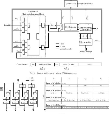
Figure 3 describes our compact coprocessor based on an
by the AES and the control unit mainly consists of a program ROM, an instruction decoder, and a program counter. In this work, we show that a careful organization of the chaining variable Vi and the message block Mi in the register file
allows one to design a control unit based on a 4-bit counter, an 8-bit counter, and a simple Finite State Machine (FSM).
ShiftRows and BIG.ShiftRows operations are implemented by accordingly addressing the register file and do not require dedicated hardware. We slightly modified an AES encryption round in order to support theBIG.MixColumnsandBIG.Final
steps.
A. TheSubBytesStep
The SubBytes step is the only non-linear transformation of the AES. Each byte ai,j of the state is considered as a
polynomial belonging toF28. AnS-Boxcomputes the modular
inverse ofa−i,j1(the value00is mapped onto itself) and then ap-plies an affine transformation [3]. This step is often considered as the most critical part of the AES and several architectures for the S-Box have already been described in the literature (see for instance [7] for a comprehensive bibliography). On Xilinx Virtex-5 FPGAs, the best design strategy consists in implementing theS-Boxas a large multiplexer controlled by
ai,j [8]. AnS-Boxfits in only 32 6-input LUTs.
B. TheMixColumnsand BIG.MixColumnssteps
Since the BIG.MixColumns step involves only Mix-Columns operations, a multiplexer allows us to bypass the
S-Box. Recall that the MixColumns step is a permutation operating on the AES state column by column: each column is considered as a polynomial overF28 and multiplied modulo
x4+1byc(x) = 03·x3+01·x2+01·x+02[3]. This operation
is performed by multiplying each column of the AES state by the following circulant matrix (all operations are performed in F28 ∼=F2[y]/(y8+y4+y3+y+ 1)):
r0 r1 r2 r3
=
02 03 01 01
01 02 03 01
01 01 02 03
03 01 01 02
·
a0 a1 a2 a3
.
Since we emphasize reducing the usage of FPGA resources, we designed a Multiply-Accumulate unit and compute the above equation in four clock cycles (Figure 4). Therefore, we need 16 clock cycles to update the four columns of an AES state. A single control bit allows one to enable or disable the feedback loop.
C. TheAddRoundKeyand BIG.Final steps
Our MixColumns unit outputs four bytes that we store in a shift register. This approach allows us to write the result in the register file byte by byte. Since we focus on Virtex-5 FPGAs, we can take advantage of the6-input LUT associated with each flip-flop and perform an optional AddRoundKey
step without increasing the slice count (Figure 5). When the control bitctrl5is set to1, a subkey is combined with the AES
state by means of a bitwise exclusive OR operation. Eight
additional 6-input LUTs derive the new output value of the chaining variable. During the BIG.Final step, two bytes are read from the register file, added and accumulated thanks to the feedback mechanism enabled by the control bitctrl3.
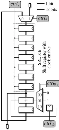
Shift register LUTs with a clock enable (SRL16E primitive) store the subkeys while minimizing the number of slices of our coprocessor (Figure 6). The choice of a32-bit datapath enables to provide the AddRoundKey with four 8-bit sukbeys ski, 0 ≤i ≤3 at each clock cycle, and to increment the internal counter κ in two clock cycles, thus keeping the critical path as short as possible.
10 1bit
32bits
ctrl9:8
1 0
01 00 ctrl7
ctrl6
Shift
re
gister
with
ctrl10
clock
enable
0 1
SRL16E
Fig. 6. Implementation of the key schedule. Control bitsctrl7 and ctrl10
denote clock enable signals.
D. Register File
Recall that we need to store three blocks of256bytes in the memory of the coprocessor. The first one stores the chaining variableVi−1and the message blockMineeded to perform the BIG.Finalstep. Two further blocks are allocated to the internal state: during MixColumnsoperations, data are read from one of them and results are written into the other one. The total amount of memory is therefore 768bytes, and a single block of dual-ported memory allows us to implement our register file on a Virtex-5 FPGA (RAMB18 primitive). The initial chaining variableV0and the message blocksMi,1≤i≤t, are written
on port A. In order to avoid multiplexers (and to keep the size of the circuit as small as possible), the data computed during the BIG.SubWords,BIG.MixColumns, and BIG.Finalsteps are written on port B. Since ourMixColumnsunit processes a single input byte at each clock cycle, we need a single port to read data during the BIG.SubWords and BIG.MixColumns
operations. However, in order to speed up theBIG.Finalstep, we read data from ports A and B.
1
0 we0
MixColumns Data
addr0
addr1
we1
Port B
ctrl
0
addr1(10bits)
ctrl
1
ctrl
5:2
Control signals 32bits 8bits
Control unit User interface
Control word: Data
ctrl10:6 (dual-ported memory block)
Register file
S-box
Round subkeys Key schedule
Port
B
sk1 sk2 sk3 sk0
Port
A
AddRoundKey andBIG.Final
ctrl10:0
we0
Port A addr0(10bits)
we1
Fig. 3. General architecture of a8-bit ECHO coprocessor.
ctrl1
×02 1bit 8bits
×03
T
ime
r1
2a0⊕3a1⊕a2 a0⊕2a1⊕3a2 a0⊕a1⊕2a2 r2
2a0⊕3a1⊕a2⊕a3
r3
a0⊕2a1⊕3a2⊕a3
2a0
a0⊕a1⊕2a2⊕3a3 Input of MixColumns:a0
3a0⊕a1⊕a2⊕2a3 Input of MixColumns:a1
Input of MixColumns:a2
Input of MixColumns:a3
3a0 a0
a0⊕2a1 a0⊕a1 3a0⊕a1 2a0⊕3a1
r0 r1 r2 r3
a0 r0
3a0⊕a1⊕a2
Fig. 4. Implementation ofMixColumns.
4j+i in the the block specified by the two most significant bits of the address (Figure 1).
E. Control Unit
Our control unit generates the eleven control bitsctrl10:0of
the processing units, and addressesaddr0andaddr1. It mainly
consists of a simple FSM (13 states), a3-bit round counter, and two specific counters that output the eight least significant bits of the read and write addresses (i.e. the position of the byte a(k)i,j in a block of 256 bytes; the two most significant bits defining in which block we read/write the data are easily computed by the FSM). We will focus here on the address generation process, which was the most challenging task in the design of our compact architecture: the addressing schemes of
the BIG.SubWords,BIG.MixColumns, and BIG.Finalsteps seem very different at first. However, we found a way to generate all read and write addresses with only one counter by 5modulo16and one modulo-256counter.
Since we combineShiftRowsandMixColumnsoperations during theBIG.SubWords step, we compute:
˜
a0,j(k),˜a(k+1)1,j ,a˜(k+2)2,j ,˜a(k+3)3,j
←MixColumnsa(k)0,j, a(k)1,(j+1) mod 4,
a(k)2,(j+2) mod 4, a(k)3,(j+3) mod 4,
From
ctrl
5ctrl
2ctrl
3ctrl
41bit
8bits
6
-input LUTs
5
-input LUTs
5-input LUTs
3-input LUTs
sk1 sk2 sk3
1 0
1 0 1 0 1 0
register file
To register file
MixColumns
sk0
Fig. 5. Implementation ofAddRoundKeyandBIG.Final.
position of aa(k)0,j in the AES stateAk). We check that we have
to increment this address by 5 modulo16 in order to obtain the four least significant bits of the read addresses of a(k)1,j,
a(k)2,j, and a(k)3,j (Figure 7a). Since a MixColumns operation takes 16 clock cycles, we have to increment the four most significant bits of the read address every 16 clock cycles. It suffices to consider the four most significant bits of a
modulo-256 counter to achieve this task. Recalll that MixColumns
steps update each AES state Ai, 0 ≤ i ≤ 15, column by
column. Thus, thanks to our organization of the bytes a(k)i,j
in the memory, the same modulo-256 counter allows us to generate write addresses.
During the BIG.MixColumns step, we have to increment the read addresses by80modulo256(Figure 7b). Since80 = 5·16, we can re-use our counter by5modulo16to compute the four most significant bits of the read address. The write address is incrementd by 16 modulo 256 at each clock cycles. The four least significant bit of the modulo256 counter allow us to perform this operation. After16clock cycles, these counters go back to their initial value and we have to increment the read and write addresses by one. Thus, the four most significant bits of the modulo-256counter provide us with the four least significant bits of these addresses.
Recall that we read two bytes at each clock cycle during the BIG.Final step. Let us denote byB(k), 0≤k≤15, the 128-bit words of the4×4array storing the chaining variable
Vi−1 and the message block Mi. In order to update a byte
of the chaining variable, we compute the bitwise exclusive OR ofa(k)i,j,a(k+4)i,j ,a(k+8)i,j ,a(k+12)i,j ,b(k)i,j,b(k+4)i,j ,b(k+8)i,j , and
b(k+12)i,j , where 0≤k≤3. Starting from the address of a(k)i,j
(or b(k)i,j since we only consider the address of a byte in an array of 256 bytes), we have to increment it by 64 at each clock cycles. The least significant bit is incremented by one every four clock cycles in order to process the next byte of the internal state. Since we overwrite Vi−1, the generation of
write addresses is straightforward during the BIG.Final step. These observations allow for the design of a compact address generator for our coprocessor (Figure 8). It mainly consists of a counter by 5 modulo 16 and a modulo-256
counter. Two multiplexers select read and write addresses according to two control bits specifying the current operation (BIG.ShiftRows, BIG.MixColumns, or BIG.Final). Recall that our coprocessor embeds several pipeline stages (Figure 3):
• The read address is stored in an internal register of the dual-ported memory block.
• The data at the specified address is stored in the output register on port A.
• TheMixColumnsoperations is performed in an iterative fashion and requires four clock cycles.
• Our AddRoundKey unit stores its outcome in a shift-register before sending it to the shift-register file.
Consequently, the write operation occurs seven clock cycles after the corresponding read operation. It is therefore necessary to delay write addresses by seven clock cycles. Figure 9 describes our address generation scheme. For each operation, we have to generate256read and write addresses (except in the BIG.final step where only64bytes are written in the register file). Since our two counters are incremented modulo 16and
A1 A5 A8
a(0)3,3 a(0)3,2 a(0)3,1
a(0)0,3
A9 A12
A13 a(0)0,2
a(0)1,2
A2 A6
A3 A7 A11
A10 A14 A15 005 010 001 002 000 004 006 003 ˜ A0 ˜ A1 ˜ A4 ˜ A5 ˜ A8 ˜ A9 ˜ A12 ˜ A13 ˜ A2 A6˜
˜
A3 A7˜ A11˜ ˜ A10 A14˜
˜ A15 014
013
˜ a(0)3,0 015
˜ a(0)2,3
011
˜ a(0)1,3
007
012
a(0)1,1
˜ a(0)3,3 a(0)2,2
008
005
010 001
˜ a(0)3,2 002
˜ a(0)3,1
˜ a(5)0,3
˜ a(6)0,3
˜ a(7)0,3 000
˜ a(0)0,3 004
˜ a(0)0,2
006
003 a(0)3,0
014 ˜ a(0)1,2
013
a(0)1,0 ˜a(0)1,1
a(0)2,0
015 a(0)0,0
˜ a(0)2,2 ˜
a(0)1,0 a(0)0,1
a(0)2,3 a(0)2,1
011 009
˜ a(0)2,0
007 ˜ a(0)0,0
012 ˜
a(0)0,1
156 076 060 236 076 092 108 124 a(9)0,3
a(4)0,3
a(3)0,3
a(14)0,3
˜ a(4)0,3
008
˜ a(0)2,1 a(0)1,3
(a)ShiftRowsandMixColumns
009
(b)BIG.ShiftRowsandBIG.MixColumns
A0 A4
Fig. 7. Address generation duringBIG.SubWordsandBIG.MixColumns.
our address generation scheme avoids memory collisions). Each round involves twoMixColumnssteps (BIG.SubWords) and aBIG.MixColumnsstep. Therefore, the total number of clock cycles for eight rounds is equal to8·3·256 = 6144.
3
:
0
Modulo-256counter Modulo-16counter
1 : 0 7 : 2 01 10 00 7 : 4 7 : 4 01 10 00
00: BIG.SubWords 01: BIG.MixColumns 10: BIG.Final
Write address
Read address
SRL16 7-stage
shift re gister 8bits 1 4bits 5 7 : 2 7 : 4
Fig. 8. Address generator based on a modulo-16counter and a modulo-256 counter.
The BIG.Final step requires careful attention: in order to speed up this operation, we read a byte of Vi−1 or Mi on
port A, and a byte of the internal state (i.e. the output of the eighth round) on port B at each clock cycle. Due to the internal pipeline stages of our architecture, the computation of a byte ofVi also requires seven clock cycles. However, we
have to wait for the end of the write cycle before processing the next byte and the total number of clock cycles is given by
64·7 + 1 = 449(one additional cycle is required to complete the last write cycle and reset the FSM before processing the next compression function).
IV. RESULTS, COMPARISONS,ANDFUTUREWORK
We captured our architectures in the VHDL language and prototyped our coprocessors on a Virtex-5 FPGA with average speedgrade. Table II summarizes our place-and-route results. A bunch of articles about ASIC and FPGA implementations of ECHO are available in the SHA-3Zoo [9]. However, most of them focus on high-speed parallel implementations [10]– [13], and it is difficult to compare our work against such designs. To the best of our knowledge, the only compact coprocessor reported in the literature is the one by Lu et al. [12]. Unfortunately for our comparison, they only describe an ASIC implementation.
208 32 112
128 144 160
15 95 175 255 79 159 239 63
127 111 95 79 63 47 31 15
143 223 47 127
143 159 175 191
207 31 111 191
207 223 239 255
0 16 32 48
0 80 160 240 ˜ A0
0 1 2 3 4 5 6 7 8 9 10 11 12 13 14 15 240241 242243244 245246247 248249250 251252253 254255
0 5 10 15 4 9 14 3 8 13 2 7 12 1 6 11 0 5 10 15 4 9 14 3 8 13 2 7 12 1 6 11
A15 A˜15 A15 A˜15 A15 A˜15 A15 A˜15
0 1 2 3 4 5 6 7 8 9 10 11 12 13 14 15 240241 242243244 245246247 248249250 251252253 254255
11 240 245 250 255 244 249 254 254 248 253 242 247 252 241 246 251
0 5 10 15 4 9 14 3 8 13 2 7 12 1 6
176 192 16 96
176 192 208 224 240 64 144 224 48
64 80 96 112
128
1 1 1 2 2 2 2 3 3 3 3
0 64 128 192 1 65 129 193 2 66 130 194 3 67 131 195
0 0 0 0 60 60 60 60 61 61 61 61 62 62 62 62 63 63 63 63
60 124 188 252 61 125 189 253 62 126 190 254 63 127 191 255 BIG.Final
Write addresses: Read addresses:
1
Modulo-256counter:
Modulo-16counter:
BIG.SubWords
Write addresses: Read addresses:
A0 A0 A˜0 A0 A˜0 A0 A˜0
BIG.MixColumns
Write addresses: Read addresses:
TABLE II
COMPACT IMPLEMENTATIONS OFSHA-3CANDIDATES ONVIRTEX-5 FPGAS.
Algorithm FPGA [slices]Area Memoryblocks Frequency[MHz] Throughput[Mbps] This work ECHO-224/256 xc5vlx50-2 127 1 352 72
Beuchatet al.[14] BLAKE-32 xc5vlx50-2 56 2 372 225
Aumassonet al.[15] BLAKE-32 xc5vlx110 390 – 91 575
Beuchatet al.[14] BLAKE-64 xc5vlx50-2 108 3 358 314
Aumassonet al.[15] BLAKE-64 xc5vlx110 939 – 59 533
Bertoniet al.[16] Keccak xc5vlx50-3 448 – 265 52
Baldwinet al.[17] Shabal xc5vlx220-2 2307 – 222.22 1330
Feron and Francq [18] Shabal not specified 596 – 109 1142
Detreyet al.[19] Shabal xc5vlx30-2 153 – 256 2051
compact coprocessor (at the price of an extra memory block). In spite of a high clock frequency, the throughput is however quite disappointing when compared to other candidates.
The main advantage of ECHO is that it is based on the round function of the AES. We plan to modify our architecture to support AES encryption, AES decryption, and ECHO. Figure 10 describes the general architecture of our processing unit. On Virtex-5 devices, the MixColumns and InvMix-Columnsunits require the same number of slices. Thus, there is no need to exploit the relation between the MixColumns
polynomialc(x)and theInvMixColumnspolynomiald(x)[3, p. 55]. A few control bits allow one to configure the datapath of the coprocessor in order to perform the desired operation. We will design a control unit for this architecture in future work.
0
InvMixColumns
1 0
Control signals
8bits BIG.Final
1 0
1 0
1 0
Subkey register file
From
T
o
re
gister
file
MixColumns
1 0
SubBytes
InvSubBytes
1
Fig. 10. A coprocessor for AES encryption, AES decryption, and ECHO.
REFERENCES
[1] R. Benadjila, O. Billet, H. Gilbert, G. Macario-Rat, T. Peyrin, M. Rob-shaw, and Y. Seurin, “SHA-3 proposal: ECHO,” 2009, available online at http://crypto.rd.francetelecom.com/echo.
[2] J. Zhai, C. Park, and G.-N. Wang, “Hash-based RFID security protocol using randomly key-changed identification procedure,” inComputational Science and Its Applications–ICCSA 2006, ser. Lecture Notes in Com-puter Science, M. Gavrilova, O. Gervasi, V. Kumar, C. K. Tan, D. Taniar, A. Lagan`a, Y. Mun, and H. Choo, Eds., no. 3983. Springer, 2006, pp. 296–305.
[3] J. Daemen and V. Rijmen,The Design of Rijndael. Springer, 2002. [4] R. Benadjila, O. Billet, S. Gueron, and M. Robshaw, “The Intel AES
instructions set and the SHA-3candidates,” inAdvances in Cryptology– ASIACRYPT 2009, ser. Lecture Notes in Computer Science, M. Matsui, Ed., no. 5912. Springer, 2009, pp. 162–178.
[5] B. Baldwin, A. Byrne, L. Lu, M. Hamilton, N. Hanley, M. O’Neill, and W. Marnane, “A hardware wrapper for the SHA-3 hash algorithms,” 2010, cryptology ePrint Archive, Report 2010/124.
[6] T. Good and M. Benaissa, “AES on FPGA from the fastest to the smallest,” in Cryptographic Hardware and Embedded Systems–CHES 2005, ser. Lecture Notes in Computer Science, J. R. Rao and B. Sunar, Eds., no. 3659. Springer, 2005, pp. 427–440.
[7] K. Gaj and P. Chodowiec, “PGA and ASIC implementations of the AES,” inCryptographic Engineering, C¸ .K. Koc¸, Ed. Springer, 2009, pp. 235–294.
[8] P. Bulens, F.-X. Standaert, J.-J. Quisquater, P. Pellegrin, and G. Rouvroy, “Implementation of the AES-128 on Virtex-5 FPGAs,” in Progress in Cryptology–AFRICACRYPT 2008, ser. Lecture Notes in Computer Science, S. Vaudenay, Ed., no. 5023. Springer, 2008, pp. 16–26. [9] “The SHA-3 zoo,” http://ehash.iaik.tugraz.at/wiki/The SHA-3 Zoo. [10] M. Kinsy and R. Uhler, “SHA-3: FPGA implementation of ESSENCE
and ECHO hash algorithm candidates using Bluespec,” available at http: //csg.csail.mit.edu/6.375/6 375 2009 www/projects/group1 report.pdf. [11] K. Kobayashi, J. Ikegami, S. Matsuo, K. Sakiyama, and K. Ohta, “Evaluation of hardware performance for the SHA-3candidates using SASEBO-GII,” 2010, cryptology ePrint Archive, Report 2010/010. [12] L. Lu, M. O’Neill, and E. Swartzlander, “Hardware evaluation
of SHA-3 hash function candidate ECHO,” available at http://www.ucc.ie/en/crypto/CodingandCryptographyWorkshop/ TheClaudeShannonWorkshoponCodingCryptography2009/ DocumentFile,75649,en.pdf.
[13] S. Tillich, M. Feldhofer, M. Kirschbaum, T. Plos, J.-M. Schmidt, and A. Szekely, “High-speed hardware implementations of BLAKE, Blue Midnight Wish, CubeHash, ECHO, Fugue, Grøstl, Hamsi, JH, Keccak, Luffa, Shabal, SHAvite-3, SIMD, and Skein,” 2009, cryptology ePrint Archive, Report 2009/510.
[14] J.-L. Beuchat, E. Okamoto, and T. Yamazaki, “Compact implementations of BLAKE-32 and BLAKE-64 on FPGA,” 2010, cryptology ePrint Archive, Report 2010/173.
[15] J.-P. Aumasson, L. Henzen, W. Meier, and R.-W. Phan, “SHA-3 proposal BLAKE (version 1.3),” 2009, available online at http://www.131002.net/ blake.
[16] G. Bertoni, J. Daemen, M. Peeters, and G. V. Assche, “Keccak sponge function family main document (version 2.0),” 2009, available online at http://keccak.noekeon.org.
[17] B. Baldwin, A. Byrne, M. Hamilton, N. Hanley, R. McEvoy, W. Pan, and W. Marnane, “FPGA implementations of SHA-3 candidates: CubeHash, Grøstl, LANE, Shabal and Spectral Hash,” 2009, cryptology ePrint Archive, Report 2009/342.
[18] R. Feron and J. Francq, “FPGA implementation of Shabal: Our first results,” 2010, available online at http://www.shabal.com.

![Fig. 2.Chained iteration of the compression function. T denotes the optionaltruncation described in [1, Section 3.5] and [1, Section 4.1].](https://thumb-us.123doks.com/thumbv2/123dok_us/1871723.1243582/2.595.40.295.50.138/chained-iteration-compression-function-optionaltruncation-described-section-section.webp)