University of Windsor University of Windsor
Scholarship at UWindsor
Scholarship at UWindsor
Electronic Theses and Dissertations Theses, Dissertations, and Major Papers
2016
A Hardware Security Solution against Scan-Based Attacks
A Hardware Security Solution against Scan-Based Attacks
Ankit Mehta
University of Windsor
Follow this and additional works at: https://scholar.uwindsor.ca/etd
Recommended Citation Recommended Citation
Mehta, Ankit, "A Hardware Security Solution against Scan-Based Attacks" (2016). Electronic Theses and Dissertations. 8002.
https://scholar.uwindsor.ca/etd/8002
This online database contains the full-text of PhD dissertations and Masters’ theses of University of Windsor students from 1954 forward. These documents are made available for personal study and research purposes only, in accordance with the Canadian Copyright Act and the Creative Commons license—CC BY-NC-ND (Attribution, Non-Commercial, No Derivative Works). Under this license, works must always be attributed to the copyright holder (original author), cannot be used for any commercial purposes, and may not be altered. Any other use would require the permission of the copyright holder. Students may inquire about withdrawing their dissertation and/or thesis from this database. For additional inquiries, please contact the repository administrator via email
A Hardware Security Solution against Scan-Based Attacks
By
Ankit Mehta
A Thesis
Submitted to the Faculty of Graduate Studies
through the Department of Electrical and Computer Engineering in Partial Fulfillment of the Requirements for
the Degree of Master of Applied Science at the University of Windsor
Windsor, Ontario, Canada
2016
© 2016 Ankit Mehta
All rights reserved INFORMATION TO ALL USERS
The quality of this reproduction is dependent upon the quality of the copy submitted. In the unlikely event that the author did not send a complete manuscript
and there are missing pages, these will be noted. Also, if material had to be removed, a note will indicate the deletion.
All rights reserved.
This work is protected against unauthorized copying under Title 17, United States Code Microform Edition © ProQuest LLC.
ProQuest LLC.
789 East Eisenhower Parkway P.O. Box 1346
Ann Arbor, MI 48106 - 1346 ProQuest
Published by ProQuest LLC ( ). Copyright of the Dissertation is held by the Author. ProQuest Number:
10182906 10182906
A Hardware Security Solution against Scan-Based Attacks
by
Ankit Mehta
APPROVED BY:
______________________________________________ Dr. Ahmed Azab
Mechanical, Automotive & Materials Engineering
______________________________________________ Dr. Huapeng Wu
Electrical and Computer Engineering
______________________________________________ Dr. Rashid Rashidzadeh, Supervisor
Electrical and Computer Engineering
______________________________________________ Dr. Majid Ahmadi, Supervisor
Electrical and Computer Engineering
iii
DECLARATION OF CO-AUTHORSHIP/PREVIOUS PUBLICATION
I. Co-Authorship Declaration
I hereby certify that this thesis incorporates the outcome of joint research in collaboration with, and
under the esteemed supervision of Dr. Rashid Rashidzadeh and Dr. Majid Ahmadi.
I am aware of the University of Windsor Senate Policy on Authorship and I certify that I have
properly acknowledged the contribution of other researchers to my thesis, and have obtained written
permission from each co-author(s) to include the above material(s) in my thesis. I certify that, with the
above qualification, this thesis, and the research to which it refers is the product of my own original work.
II. Declaration of Previous Publication
This thesis includes 3 original papers that have been previously published /submitted for publication in
peer reviewed journals as follows:
Thesis Chapter Publication Title/ full citation Publication Status
All Chapters Title: “ A Hardware Security Solution
against Scan based attacks”, 2016, IEEE
Int’l Symposium on Circuits and Systems
Accepted
All Chapters Title: “ A Secure Test solution for Sensor
Nodes containing crypto cores”
iv
All Chapters Title: “A hardware secure solution for scan
enabled circuits using access control”
Submitted
I certify that, to the best of my knowledge, my thesis does not infringe upon anyone’s
copyright, nor violate any proprietary rights. Any ideas, techniques, quotations, and material
appertaining to other people included in my thesis, published or otherwise, are fully acknowledged
in accordance with standard referencing practices. Furthermore, to the extent that I have included
copyrighted material that surpasses the bounds of fair dealing within the meaning of the Canada
Copyright Act, I certify that I have obtained a written permission from the copyright owner(s) to
include such material(s) in my thesis and have included copies of such copyright clearances in my
appendix.
I certify that I have obtained written permission from the copyright owner(s) to include the
above published materials in my thesis. I certify that the above material describes work completed
during my registration as graduate student at the University of Windsor.
I declare that this is a true copy of my thesis, including any final revisions, as approved by
my thesis committee and the Graduate Studies office, and that this thesis has not been submitted
v ABSTRACT
Scan based Design for Test (DfT) schemes have been widely used to achieve high fault coverage
for integrated circuits. The scan technique provides full access to the internal nodes of the
device-under-test to control them or observe their response to input test vectors. While such
comprehensive access is highly desirable for testing, it is not acceptable for secure chips as it is
subject to exploitation by various attacks. In this work, new methods are presented to protect the
security of critical information against scan-based attacks. In the proposed methods, access to the
circuit containing secret information via the scan chain has been severely limited in order to reduce
the risk of a security breach. To ensure the testability of the circuit, a built-in self-test which utilizes
an LFSR as the test pattern generator (TPG) is proposed. The proposed schemes can be used as a
countermeasure against side channel attacks with a low area overhead as compared to the existing
vi DEDICATION
I would like to dedicate this thesis to my family my late grandfather Ainshi Lal Mehta and late
grandmother Lajwanti Mehta. Your blessings and the values you taught me made this possible. I
miss you a lot and still remember the good old days. In addition to this, I would like to dedicate
my work to my parents and my cousin brother. Special thanks to my parents, Mr. Sanjay Mehta
and Mrs. Sonia Mehta, for always supporting me to pursue my master’s degree and my loving,
sweet younger sister, Manya Mehta, who is very good and her constant motivation helped me to
achieve my master’s degree. No matter how far I go in my life, this would not have been possible
without all of you.
I would also like to thank my cousin brother, Dr. Bhuvanender Vashist (Sonu Bhaiya), for always
motivating me to continue my studies and making me realize the importance of a degree from
abroad. This would never have been possible had you not given me your emotional support. You
have always stood as my shield against all problems I have faced and provided the best and the
right guidance. I thank God for having you in my life and will love you forever. Last but not the
least, I would like to thank God for the person that I am today and making this master’s degree
possible.
vii
ACKNOWLEDGEMENTS
I would like to thank my supervisor, Dr. Rashid Rashidzadeh, and advisor, Dr. Majid Ahmadi,
their unbounded support, motivation, constructive comments, and motivation throughout my
master’s degree helped address even the most basic of questions. Without their support, I could
not have completed this degree. The constructive feedback which they provided helped polish my
work. I would also like to thank my other committee members, Dr. Ahmed Azab and Dr. Huapeng
viii
TABLE OF CONTENTS
DECLARATION OF CO-AUTHORSHIP/PREVIOUS PUBLICATION ... iii
ABSTRACT ... v
DEDICATION ... vi
ACKNOWLEDGEMENTS ... vii
LIST OF TABLES ... xii
LIST OF FIGURES ... xiii
LIST OF ACRONYMS ... xv
Chapter 1 Introduction and Background ... 1
1.1 Motivation and Problem Statement ... 1
1.2 Testing of Digital Circuits ... 3
1.3 VLSI Testing Challenges ... 3
1.4 Types of Testing ... 4
1.5 Test Dynamics and Fault models ... 6
1.6 Hardware Attacks and Emerging topic ... 7
1.7 Thesis Contribution ... 7
1.8 Thesis Organization ... 7
Chapter 2 Testing of VLSI circuits and Design for Testability ... 8
ix
2.2 Built in Self-Test ... 9
2.3 Test Pattern Generation ... 9
2.3.1 Standard LFSR ... 10
2.3.2 Modular LFSR ... 10
2.4 LFSR Characteristics ... 11
2.5 Mathematical Modelling of LFSRs ... 12
2.5.1 Attacks against the LFSR ... 12
2.6 Cyclic LFSRs ... 13
2.7 Exhaustive Testing ... 15
2.7.1 Complete LFSR ... 16
2.7.2 Binary Counter ... 17
2.8 Pseudo Exhaustive Testing ... 17
2.9 Pseudo Random Testing ... 17
2.9.1 Maximum-Length LFSR ... 17
2.9.2 Weighted LFSR ... 18
2.10 Segmentation Testing ... 18
2.10.1 Signature Analysis ... 19
Chapter 3 Boundary Scan and Core based testing ... 22
3.1 Introduction ... 22
x
3.3 IEEE 1149.1 Test Architecture and Working ... 24
3.4 Boundary Scan Cell, Test Circuitry and Bus protocols ... 26
3.4.1 TAP State diagram ... 27
3.5 IEEE 1500 Architecture ... 29
Chapter 4 A Hardware security solution against scan based attacks utilizing LFSR ... 35
4.1 Introduction to Hardware attacks ... 35
4.2 Literature Survey and Existing solutions in Literature ... 35
4.3 Scan Based Attacks ... 37
4.4 Proposed Method ... 38
4.5 Simulation Results ... 43
Chapter 5 A Secure test solution using BIST for crypto cores ... 44
5.1 Introduction to Core based attacks ... 44
5.2 Scan based attacks and countermeasures ... 44
5.3 Proposed Method ... 48
5.4 Complexity Analysis ... 49
Chapter 6 AHardware secure solution for scan enabled circuits using access control ... 51
6.1 Introduction ... 51
6.2 Literature Survey and Existing Solutions ... 51
6.3 Proposed Method ... 53
xi
Chapter 7 Summary Conclusions and Future work ... 58
REFERENCES ... 60
xii
LIST OF TABLES
Table 1: Table showing the generator polynomial for cyclic LFSR [10] ... 14
Table 2: Comparison of proposed architecture with existing solutions [68] ... 43
Table 3: Area overhead and comparison with existing solutions ... 57
xiii
LIST OF FIGURES
Figure 1: Various stages of Testing [90]... 2
Figure 2: Flow for testing of Digital Circuits ... 3
Figure 3: CMOS chip by IBM incorporating 6 levels of interconnections [7] ... 4
Figure 4: Flow demonstrating BIST Testing [10] ... 9
Figure 5: The n-stage conventional LFSR [10] ... 10
Figure 6: The n stage modular LFSR [10] ... 10
Figure 7: Test pattern generated by different LFSR [10] ... 11
Figure 8: Complete LFSRs (a) four-stage standard LFSR (b) four stage modular LFSR (c) Minimized version of (a) (d) Minimized version of (b) [10] ... 16
Figure 9: Binary counter used as Exhaustive Pattern Generation [10] ... 17
Figure 10: N-stage single input shift register [10] ... 19
Figure 11: N stage multiple input shift register [10] ... 20
Figure 12: Board level testing in daisy chain architecture [10] ... 23
Figure 13: IEEE 1149.1 architecture [45] ... 25
Figure 14: A Boundary Scan Cell [45] ... 26
Figure 15:16-state finite state machine to support Boundary Scan Architecture [45] ... 27
Figure 16: IEEE P1500 illustrating wrapper on different cores and TAM [48] ... 29
Figure 17: IEEE P1500 Test interface illustrating parallel and serial wrappers [48] ... 30
Figure 18: Test circuitry supporting IEEE P1500 architecture [48] ... 31
Figure 19: First 3 flip flops configured as test pattern generator [68] ... 39
xiv
Figure 21: 3-bit LFSR configured to act as test pattern generator [68] ... 41
Figure 22: Test Controller for switching between various modes of testing [68] ... 42
Figure 23: Modified 16-bit state machine supporting IEEE 1149.1 architecture [68] ... 42
Figure 24: The implemented design on cadence 65nm suite [68] ... 43
Figure 25: Steps involved in AES Encryption [70] ... 45
Figure 26: Scan based attack on AES round operation [72] ... 46
Figure 27: Architecture showing the XOR gate at random places [76] ... 47
Figure 28: Proposed Architecture showing the signature analysis ... 48
Figure 29: Proposed Architecture for controlled access ... 53
Figure 30: Measurement setup for the proposed architecture ... 55
Figure 31: Waveform if user is granted access to scan chain ... 56
Figure 32: Proposed Secure controller to switch modes ... 56
Figure 33: Waveform to support if the user is not granted access ... 57
xv
LIST OF ACRONYMS
Abbreviations/Symbols Description
IC SSI MSI LSI VLSI DfT SoC ATE DC AC ppm BIST TPG CUT Integrated Circuit
Small Scale Integration
Medium Scale Integration
Large Scale Integration
Very Large Scale Integration
Design for Test
System on Chip
Automatic Test Equipment
Direct Current
Alternating Current
Parts per million
Built-in self-test
Test Pattern Generator
xvi
Abbreviation/Symbol Description
LFSR GF EPG CFSR PRPG RP CRC SISR MISR JTAG IPs TAPC TAP
Linear Feedback Shift Register
Galois Field
Exhaustive Pattern Generator
Complete LFSR
Pseudo Random Pattern Generator
Pattern Resistant
Cyclic Redundancy Check
Single Input shift register
Multiple input shift register
Joint Test Action Group
Intellectual Property
Test Access Port Controller
xvii
Abbreviations/Symbols Description
TDI TDO TMS TCK TRST IR BSC TAM CTL WSP WSI WSO WSC
Test Data Input
Test Data Output
Test Mode Select
Test Clock
Test Reset
Instruction Register
Boundary Scan Cell
Test Access Mechanism
Core Test Language
Wrapper Serial Port
Wrapper serial Input
Wrapper Serial Output
xviii
Abbreviations/Symbols Description
WIR WPC WPI WPO WPP WBY WBR CFI CFO CTI CTO RC4 PUF
Wrapper Instruction Register
Wrapper Parallel control
Wrapper Port Input
Wrapper Port output
Wrapper Parallel port
Wrapper Bypass Register
Wrapper Boundary Register
Cell Functional input
Cell Functional Output
Cell Test Input
Cell Test output
Riveset Cipher 4
1
Chapter 1
Introduction and Background
1.1 Motivation and Problem Statement
The need to increase the processing power and speed of processors, on the other hand reducing the
price and power consumption of processors has led to decrease in the feature size of the transistors,
This, in turn, has directly affected the operating clock frequency of microprocessors. For example,
the operating frequency of current microprocessors is in the gigahertz range as compared to a few
100 KHz in the 1970s. The reductions in feature sizes and the increased number of transistors per
chip raises the probability that an IC may have manufacturing or functional defects. With feature
sizes at the nanometer scale, it is not unusual that some of the transistors in the microchip may not
work properly, and thus, causing the entire chip to malfunction [1].
Defects created at the manufacturing stage are unavoidable even if the utmost care is taken in state
of the art fabrication facilities. A popular rule of ten, which is followed in industry which states
that the cost of testing goes up as we move from wafer to chip and from chip to board level and
before it can be adopted for the system level use as shown in figure 1. Due to impossibility of
infallible design and fabrication processes involved, it is imperative to screen out faulty ICs and
defective parts so as to prevent the shipping of defective parts to customers. Testing techniques
have been developed without considering the fact that the circuit added to increase testability can
also be used to access security sensitive information. Many systems have been attacked using the
2
In this thesis, we have proposed a secure design for test techniques to counter the scan based
attacks.
1. In the first technique, two modes for testing have been proposed, namely, the secure mode
of testing and the insecure mode of testing. A controller is designed to control the transition
from the secure mode to the insecure mode of testing and vice versa.
2. In the second technique, a secure self-test technique has been proposed keeping in view the
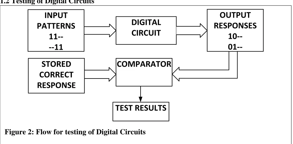
3 1.2 Testing of Digital Circuits
Figure 2 shows the flow of testing for the digital circuits. For a given device under test, the binary
test patterns are applied as the input to the circuit. The respective output responses are then
obtained. These output responses are then compared with the correct stored responses in a response
analyzer. If the responses match, then the circuit is considered to be acceptable, else the circuit is
faulty. Most of the input test vectors are applied by an apparatus called ATE (Automatic Test
Equipment) [2].The test responses are written and stored in the memory of the test equipment.
1.3 VLSI Testing Challenges
The manufacturing of VLSI devices is a complex and cumbersome process. Figure 3 shows the
image of a manufactured IC in which the channel length is 120 nm and there are six levels of
interconnections and wirings. There are many stages in the IC manufacturing process. In this
particular process, some random manufacturing imperfections can cause variations in the process, Figure 2: Flow for testing of Digital Circuits
4
voltage and temperature in the final manufactured IC. Variations affecting transistor channel
length, the metal interconnect width and thickness, and dielectric thickness can be grouped under
process variations [11-13].
1.4 Types of Testing
Testing methodology changes depending on the production stage at which an IC being tested. In
the initial stage of production, for instance, after the wafers have been manufactured, wafer sort
testing is performed. The motive to test at this stage is to sort out the faulty wafers [3, 4]. The
remaining wafers which are deemed to be satisfactory are then processed to the next stage for
packaging. While the sorting of wafers is performed, the characterization test is also conducted.
Broadly, the test can be classified as follows:
5
1. Functional Tests: In these type of tests, the input test vectors are applied and then the
responses are compared. The motive is to check the correct functionality of the device
under test. Many manufacturing faults (stuck at faults) are covered by this technique of
testing.
2. Parametric Tests: This type of testing can be categorized as a DC parametric test and an
AC parametric test. The former consists of an open test, a short test, a leakage test and a
threshold test whereas the latter entails refresh and pause time tests, rise and fall time tests,
a speed test, and setup and hold tests. The test standards which have been designed do not
depend upon the technology node being tested and hence, are independent of the
technology being tested.
3. Structural Tests: In this approach, the circuit under test is mainly tested by fault models
based on the knowledge of the structural information of the device under test. Adopting
structural testing can save time and increase the test efficiency significantly. Any specific
fault model adopted in the structural testing does not guarantee the detection of all the
possible faults in the circuits but can be quantified by the term fault coverage.
At this point, it is important to highlight the notable differences involved in the testing of ICs and
memory. The test methodology for memories fall in the paradigm of functional testing, which is
designed to cover attributes such as address decoder speed, cell coupling, data sensitivity, write
operation, and address uniqueness. To achieve extensive fault coverage, it demands long test
vector sequences.
Chip level testing and board level testing have many differences. In board level testing, the
components are previously tested and embedded. One of the aims in board level testing is to check
6 1.5 Test Dynamics and Fault models
A fault in a manufactured IC can be defined as a defect which results due to a physical condition
which prevents the circuit from performing in the desired manner. A Failure can be termed as a
deviation from the expected performance of an IC; it expresses a need for repair so as to obtain the
intended device output. A circuit error can be defined as the wrong output signal from the
defective circuit. Fault models are used to generate and compare the test vectors for the device
under test. When modeling a fault model, it is important to consider the following points:
1. The fault model should be efficient in terms of the number of test patterns and test vector
generation.
2. The fault model must be capable of predicting the behavior of the circuit under test.
The fault model can be divided into two categories, namely, the single fault model and the multiple
fault model. The single fault model can be described as
Number of single faults = 𝑘 × 𝑛 (1)
where k signifies the type of faults and n signifies the possible fault sites which can be present in
the digital circuit. However, in the practical scenario, there are commonly multiple faults in the
device-under-test and is given by
Number of multiple faults=(𝑘 + 1)𝑛 − 1 (2)
As shown in the equation 2 the circuit can have the 𝑘 possible faults. The “-1” term represents the
fault free circuit. In the single fault model two or more faults can result in the same faulty behaviors
for all the patterns .However, these faults can be termed as equivalent faults. Under this
assumption the total number of vectors to be actually considered for the given circuit are much
7
vectors is termed as fault-collapsing. By following the fault collapsing algorithms, fault simulation
times and the test time for circuits with large value of n are reduced [8-10].
1.6 Hardware Attacks and Problem Statement
Over many years, test interfaces have been built to test digital circuits. It was not known that the
interfaces for testing could pose a security threat to the device under test. Many systems have been
attacked using the controllability and observability provided by the advanced test techniques
developed over past decades. To some level, the designer can prevent the system from being
hacked by these DfT techniques and thus, can eventually reduce the system exploitation by
applying various defenses. There is a strong need for the protection of crypto chips and the
prevention of misuse of intellectual property without the inventor’s knowledge. This thesis focuses
upon the protection of hardware from scan based attacks and three solutions have been proposed
for different scenarios of testing.
1.7 Thesis Contribution
The contributions of this thesis can be summarized as follows:
novel secure design for test techniques have been proposed for digital circuits;
the area overhead for the proposed secure test techniques are negligible ; and
the proposed secure techniques do not compromise the fault coverage which many
existing techniques do.
1.8 Thesis Organization
The thesis contains a total of 7 chapters. In chapter 1, the introduction motivation and testing
challenges is discussed and hardware security is discussed. In Chapter 2 various test techniques
are discussed. Chapter 3 discusses about IEEE 1149.1 and P1500 standard. In chapters 4 to 6 secure
hardware methods are discussed. Chapter7 concludes with the summary, conclusion and future
8
Chapter 2
Testing of VLSI Circuits and Design for Testability
2.1 Introduction
Design for test techniques are used in integrated circuits to make the design testable while reducing
the cost of testing. To physically realize the design for test techniques, extra hardware is usually
required; this extra hardware is realized in the form of logic gates which are directly connected to
the internal logic or the core logic to be tested. The advantages of using the DfT techniques include:
(a) increased fault coverage; (b) making the circuit easier to control and observe; (c) reduced
testing time; and (d) supporting the hierarchical testing for logic.
The product quality of integrated circuits is quantified by various terms such as Defect, Yield and
Defect Level. A defect can be defined as a fabrication problem caused by the manufacturing
process. The defect on the wafer can be caused by process variation the impurities in wafer material
and chemicals, dust particles in the projection system, or mask misalignment. Yield is defined as
the fraction or the percentage of good chips produced in the system out of the total chips produced
in a batch of manufacturing chips. Defect level is the metric which is used to characterize the
effectiveness of the test type and the manufactured product quality achieved. It is the ratio of the
faulty chips to the chips which have passed the tests. The unit used to measure the defect level is
9 2.2 Built in Self-Test
Figure 4 shows a typical setup for built in self-test (BIST), which consists of a test pattern generator
(TPG) for generating the test patterns, circuit under test (CUT) which needs to be tested, and a
response analyzer which analyzes the response obtained from the circuit under test and compares
it with the golden signature. For controlling all the operations of BIST, there is a BIST controller
which is responsible for switching between the various states. Using BIST is advantageous as; it
eliminates the need for the external tester, supports at speed testing which helps to detect delay
faults, and it also helps to reduce test time and tester memory requirements. One of the problems
associated with built-in self-test as a method of testing is that the BIST should be able to deal with
the unknown values X [8-9].
2.3 Test Pattern Generation
The most commonly used test pattern generators for BIST applications are linear feedback shift
registers (LFSRs) which are also used for exhaustive testing, pseudo exhaustive testing, and
10
coverage, exhaustive testing is used. The various possible configurations of LFSR are discussed
in the proceeding sections. [15].
2.3.1 Standard LFSR
Figure 5 shows the configuration of the conventional LFSR. It is made up of n D-flip flops and
exclusive-OR (XOR) gates. When the XOR gates are placed on the external feedback path, it is
called external-XOR LFSR [14].
2.3.2 Modular LFSR
Figure 6 shows the modular type n stage internal feedback type LFSR with the feedback
connections in the internal type. The speed of the modular LFSR is faster as compared to the
conventional LFSR. This is due to the fact that in the conventional type configuration, each XOR
gate introduces a gate delay [14].
Figure 5: The n-stage conventional LFSR [10]
11 2.4 LFSR Characteristics
Figure 7 shows the difference in the sequence of the test patterns which is generated by the
different types of LFSR as discussed above; it is assumed that the initial contents of both types of
LFSR are set to {0001}. It is clear from the figure that for the type “a” LFSR, the sequence repeats
after 6 cycles whereas for the type “b” LFSR, the sequence repeats after 10 clock cycles [16]. The
polynomials which describe the above sequences can be described by 1+x2+x4 and 1+x+x4,
respectively. Many solutions exploiting the use of LFSR have been proposed using the advanced
design for test techniques such as broadcast scan method, variable linear decompressors, and
Illinois scan architecture [10].
12 2.5 Mathematical Modelling of LFSRs
The various possible forms of LFSRs are shown in Figure 5 and Figure 6;each has Sn flip flops, n
feedback paths, and is defined by the feedback coefficient hn. The feedback coefficient defines
whether the feedback path is active or not.
If hi = 1, the feedback path is closed or active.
If hi = 0, the feedback path is open or inactive ,
The value of the output of the flip-flop is multiplied by its coefficient pi; the result of the
multiplication depends upon whether the value of hi is 1 or 0.To begin, we can assume that the
initial value stored in the flip flops is si0, si1,…..sin-1 and the feedback connections can be defined
as h1, h2,…… hn-1.The output can be defined as sm.
𝑠𝑚 ≡ 𝑠𝑖0ℎ𝑛−1+ ⋯ + 𝑠𝑖−2ℎ2+ 𝑠𝑖−1ℎ0 𝑚𝑜𝑑 2
Following this, the next stage of the LFSR is defined as
𝑠𝑚+1 ≡ 𝑠𝑖1ℎ𝑛−1+ ⋯ + 𝑠𝑖−1ℎ2+ 𝑠𝑖ℎ0 𝑚𝑜𝑑 2
The general equation expressing the output of the LFSR can be defined as follows
𝑠𝑖+𝑚 ≡ ∑𝑚−1𝑠𝑖 ∙ ℎ𝑖+𝑗
𝑗=0 𝑚𝑜𝑑 2 ; 𝑠𝑖 , ℎ𝑗 ∈ {0, 1} , 𝑖 = 0,1,2. . .. (3) 2.5.1 Attacks against the LFSR
The inputs and the outputs from the LFSR are governed by a linear relationship. The advantage of
this linear relationship is used in communication systems. On the other hand, as a cryptosystem,
this opens opportunities for attackers. In this section, the linear relationship of the LFSR is studied
and possible attacks are also discussed. To attack an LFSR, it is assumed that the position of
13
attacker knows some bits of the plaintext and the cipher-text, as well as the knowledge of the
degree of the polynomial form the periodicity of the LFSR polynomial. The bits of the plaintext
can be described as p0, p1….. p2m-1 and the cipher-text bits can be written as c0, c1,…..c2m-1.With
the known cipher-text and plain-text bits, the attacker can construct the 2m bits
𝑠𝑖 = 𝑝𝑖+ 𝑐𝑖 𝑚𝑜𝑑 2; 𝑖 = 0,1,2 … .2𝑚 − 1 (4)
To attack the LFSR, it is imperative to know the feedback coefficients hi and the stream of the
input bits as defined by Equation 3.With the above knowledge, the attacker can generate the “m”
equations for “m” values with different values of “i” as shown by the set of equations below.
𝑖 = 0,
𝑠
𝑚≡ 𝑠
𝑖0ℎ
𝑛−1+ ⋯ + 𝑠
𝑖−2ℎ
2+ 𝑠
𝑖−1ℎ
0𝑚𝑜𝑑 2
𝑖 = 1, 𝑠
𝑚+1≡ 𝑠
𝑖1ℎ
𝑛−1+ ⋯ + 𝑠
𝑖−1ℎ
2+ 𝑠
𝑖ℎ
0𝑚𝑜𝑑 2
: ∶ ∶
∶ ∶ ∶
𝑖 = 𝑚 − 1,
𝑠
2𝑚−1≡ 𝑠
𝑖0ℎ
𝑛−1+ ⋯ + 𝑠
𝑖−2ℎ
2+ 𝑠
𝑖−1ℎ
0𝑚𝑜𝑑 2
Thus by solving above linear equations with “m” unknowns the attacker can easily find out the
feedback coefficients h0, h1,……, hm-1 by applying matrix inversion technique and Gaussian
elimination algorithm, once the feedback coefficients are found the attacker can build the LFSR
and obtain the output sequence
2.6 Cyclic LFSRs
To reduce the length of the test data, cyclic LFSRs can also be used for test generation. For cyclic
14
LFSRs are generated from the cyclic codes over the GF (2) which contains the 2k different
code-words and the n-bit tuple is realized by rotating the code-word bits to the right. The minimum
code-word or weight of cyclic LFSR is defined by “d” in cyclic LFSR [17-18].
To generate the test patterns from the cyclic LFSR, the following steps have to be followed [18]:
1. The generator polynomial g(x) has to be of greatest degree k’ (or the smallest degree k )
for generating (n’, k’)=(n’, n’-k) cyclic code that divides the 1+xn and has the distance
(design) of d ≥ w+1 [10]; and
2. The equation h(x) = (1+xn)/g(x) can be used to generate the (n’, k) cyclic code which is the
dual code of (n’, n’-k) and is generated from g(x).To construct the (n’, k) cyclic LFSR, the
following equation can be used:
𝑓(𝑥) = ℎ(𝑥)𝑝(𝑥) =
(1+𝑥 𝑛)𝑝(𝑥)𝑔(𝑥)
15
where h(x) is the parity check polynomial of g(x) which satisfies the equation g(x)*h(x) = 1+xn’.
Shortening of the equation (n’, k) cyclic LFSR to (n, k) cyclic LFSR can be achieved by deleting
the rightmost, middle or the leftmost n’-n stages from the (n’, k) cyclic LFSR which also yields the
lowest area overhead [19].
2.7 Exhaustive Testing
In exhaustive testing, the total number of 2n test patterns are applied to the circuit under test.
Generally, exhaustive testing is not preferred for combinational circuits with a large number of
inputs “n” as it takes a long time to cover all the states. A binary counter can even be used as the
exhaustive pattern generator (EPG), but the maximal length LFSRs are more efficient as compared
to the binary counters; hence, they are generally used to cover all the 2n -1 states. A right seeding
is necessary for the LFSR to generate the right test patterns [20]. A right seeding is necessary to
cover all the zero states in the test patterns of LFSR. The LFSR containing these zero states is
called the complete LFSR (CFSRs) [21]. The techniques which can be used as the pattern generator
16 2.7.1 Complete LFSR
Figure 8 (a) and 8 (b) show the application of complete LFSRs for testing a 4-input circuit under
test. The 4-stage LFSR has a period of 16 cycles. At the last stage of the complete LFSR, an XOR
gate and a NOR gate take the input from (n-1 stages) and act as a zero-detector. Using this scheme
is advantageous as it can achieve the zero state for each bit after the state of {0001}. The LFSR
presented in (a) and (b) can be minimized as shown in Figure 8 (c) and (d). The realizations shown
in (c) and (d) have the zero state after the sequence of {1000}. The advantage of using exhaustive
testing is that the detectable faults in the combinational logic will be detected. Furthermore, when
the number of inputs are small, exhaustive testing is useful, otherwise it is time consuming and not
feasible for circuits with a large number of inputs [10].
17 2.7.2 Binary Counter
Figure 9 shows the example of a binary counter used as the test pattern generator for a 4 input
combinational logic. The area overhead required by the binary counters is much larger as compared
to the conventional LFSR used as a test pattern generator [22].
2.8 Pseudo Exhaustive Testing
This type of testing requires a fewer number of test patterns as opposed to 2n test pattern required
by the exhaustive test technique for a combinational logic with “n” inputs. All the stuck at faults
can be covered by this method of testing.
2.9 Pseudo Random Testing
In this type of testing, a pseudo-random test pattern generator is used (PRPG) for generating the
pseudo random test sequences [9, 10, 15]. This type of testing can be used for combinational as
well as sequential circuits but does not give a clear idea of the fault coverage and the length of test
sequence to be used for testing. However, many schemes have been proposed to resolve this
shortcoming in [23, 24].
2.9.1 Maximum-Length LFSR
Maximal Length LFSR can be used as the pseudo random test pattern generator. The sequences
18
generating 0’s at the output. The shortcoming of using this technique is that the circuit under test
may be resistant to the random pattern which means that the probability of certain nodes receiving
the 0 or 1 value is low assuming the probability of having 0 or 1 in the input sequence is equal
[25].
2.9.2 Weighted LFSR
To solve the problem of pattern resistant faults and increase the fault coverage in RP-resistant
circuits, this method of testing is used. It uses an LFSR and a combinational circuit known as the
weighted pattern generation technique which is described in [26]. The motivation to fit the
combinational circuit between the output of the combinational circuit and the LFSR is to increase
the frequency of some patterns and decrease the frequency of certain test patterns; hence, this
technique increases the probability of detecting those faults which cannot be detected by using
simple LFSR as the test pattern generation. The method to implement this technique is discussed
in [27].This technique changes the equal distribution of maximal length LFSR so as to produce the
equal distribution weighted input sequence containing 0s and 1s which are fed to the combinational
logic under test. It adjusts the probability distribution to 0.25 or 0.75 instead of 0.5which helps in
increasing the fault coverage not covered by the 0.5 distribution model. In [28-30], good fault
coverage was obtained by assuming a probability distribution fault model.
2.10 Segmentation Testing
In the circuits where the length of the test pattern is too large or the number of inputs n is too large,
a segmentation technique or partitioning technique is followed to reduce the test time [31]. By
dividing the circuit under test into segments or partitions, this technique uses the idea of exhaustive
testing. The partitioning can be achieved in one of two ways: hardware partitioning or sensitized
19
and outputs of the sub circuits are connected to unused primary inputs and outputs of the sub circuit
under test. In sensitized partitioning, the circuit partitioning and the sub circuit isolation are
achieved by applying the input test patterns to the input lines. The process of partitioning the circuit
and testing it simplifies the overall testing process. Although the multiplexers reduce the operating
speed, the overall functionality is not altered and hence, this method is still used as an accepted
technique [33-35].
2.10.1 Signature Analysis
Signature analysis is one of the most widely used compaction techniques which is based upon the
idea of cyclic redundancy checking (CRC) [16]. This technique can be divided into two categories:
(1) serial signature analysis, which is used for compacting the output responses obtained from
the circuit under test having a single output and (2) parallel signature analysis, which is used for
compacting the responses obtained from the logic under test having multiple outputs [36-39].
1. Serial Signature Analysis Technique
In this type of technique, LFSR is used for the signature analysis and XOR gates are used for
compacting the L-bit output sequence obtained from the logic under test. Figure 10 shows an “L”
bit modular LFSR used to generate the output signature [10, 16, 43].
20
Let the L-bit message be defined as M= {m0m1m2…..mL-1} and can be written as
𝑀(𝑥) = 𝑚
0+ 𝑚
1𝑥 + 𝑚
2𝑥
2+ ⋯ + 𝑚
𝐿−1
𝑥
𝐿−1As the L-bit sequence is shifted into the modular LFSR, the remainder of the serial shift register R is given by {r0r1r2…..rn-1xn-1} expressed below as
𝑟(𝑥) = 𝑟
0+ 𝑟
1𝑥 + 𝑟
2𝑥
2+ ⋯ + 𝑟
𝑛−1
𝑥
𝑛−1The above response analyzer works as the CRC code generator [39]. Assuming that the LFSR is
defined by the characteristic polynomial f(x) then the polynomial division can be defined as
𝑀(𝑥) = 𝑞(𝑥)𝑓(𝑥) + 𝑟(𝑥)
The final signature obtained from the SISR is the remainder r(x) of the polynomial division.
2. Parallel Signature Analysis Technique
Other response analysis techniques such as transition count testing, ones counting, and the serial
signature technique require a significant area overhead for testing an output with n-bit
21
input signature analysis technique, n-XOR gates are used in combination with the modular LFSR
so as to compact the n L-bit output sequences from M0 to Mn-1. In [40-42], it is shown that the
MISR with n-inputs can be modeled as the n-input SISR if the input sequence is M(x) and the error
polynomial is E(x) as written below [41].
𝑀(𝑥) = 𝑀
0(𝑥) + 𝑥𝑀
1(𝑥) + ⋯ . . +𝑥
𝑛−2𝑀
𝑛−2
(𝑥) + 𝑥
𝑛−1𝑀
𝑛−1(𝑥)
and
𝐸(𝑥) = 𝐸
0(𝑥) + 𝑥𝐸
1(𝑥) + ⋯ + 𝑥
𝑛−2𝐸
22
Chapter 3
Boundary Scan and Core Based Testing
3.1 IntroductionThe standard for the Boundary scan based testing is IEEE 1149.1 standard, also known as the
JTAG standard. The standard was developed for testing of digital circuits on the board level and
the standard is also used for testing integrated circuits. The standard has also an extension by the
name of IEEE 1149.6 standard and is used for the prototyping of input/output high speed networks
[44].
To address the problems related to testing the core based ICs where the intellectual
properties (IPs) act as the building blocks, a different standard is developed which is analogous to
the IEEE 1149.1 standard. The standard for core based testing is known as P1500 standard
approved by IEEE in 2005.Most of the features in this standard are similar to that of the IEEE
1149.1 standard. Various features are supported by this core based testing standard such as design
reusability, plug and play features, and hierarchical test features [10].
In this chapter, both standards are discussed in detail and a comparison is also made between
the two widely known industry standards. The attacker can take the advantage of the full
controllability and observability provided by these standards and attack the device under test while
23 3.2 IEEE 1149.1 Boundary Scan Standard
As shown in figure 12, the boards are connected serially as defined by IEEE 1149.1 standard to
support boundary scan based testing at the board level. The motivation to call it boundary scan
structure comes from the fact that the circuit under test is surrounded by the boundary scan cells
serially so as to have good controllability and observability for the circuit under test. Those chips
which support the IEEE 1149.1 architecture can be fitted in the board level architecture through
the boundary scan registers. This protocol also supports the normal chip operations and thus,
enhances the design debugging and testing capabilities [9]. The standard also supports the
interconnect testing between the different circuits under test connected in a daisy chain architecture
[45].
24 3.3 IEEE 1149.1 Test Architecture and Working
Extra circuitry and memory is included in the IEEE 1149.1 architecture in addition to the boundary
scan cells so as to support the working of the whole IEEE standard. The internal logic, as shown
in the figure 13, is the actual circuit under test which is compliant for various designs for test
techniques such as scan based tests, built in self-test (BIST), and the boundary scan test technique.
The standard is known to consist of various modules such as
a test Access port (TAP) which is made of 5 terminals called test data input (TDI), test
data output (TDO), test mode select (TMS), test clock (TCK), and test reset (TRST);
a TAP controller (TAPC);
an associated decoder and instruction register (IR);
many registers such as bypass registers, boundary scan registers, device ID registers and
specific data registers which are used to control the signal flow; and
the TAP controller, which is a 16-bit state machines that controls the working of the state
machines [9-10].
In addition to the test access port which is defined above, the IEEE 1149.1 architecture also
consists of a 16-bit finite state machine which controls each step of the boundary scan architecture.
The instruction which needs to be executed is serially loaded onto the instruction register through
the external available TDI pin to the external user. The test signals which configure the boundary
25
Figure 13 shows the detailed structure of the serially connected board as shown in figure 12 above.
The TAP port defines the standard for the boundary scan as well as additional input/output pins.
The instructions in the boundary scan architecture are loaded through the test data input (TDI)
pin. The associated decoder controls the test instructions so as to perform boundary related scan
based tests. Additionally, there are test data registers which load the system-specific related
information (namely company name, device ID instruction). Some of the mandatory test
instructions such as SAMPLE, BYPASS, PRELOAD and EXTEST and several other instruction
sets such as RUNBIST, CLAMP, USERCODE, IDCODE, HIGHZ are also included in this
standard [45].
26
3.4 Boundary Scan Cell, Test Circuitry and Bus protocols
Figure 14 shows the detailed boundary scan cell which forms part of the long boundary scan chain.
The cell can be configured to acts as an input or output cell. For BSC as an input cell, the IN signal
is used for the chip input pad whereas for BSC as an output cell, the OUT signal is connected to
the output signal pad. The Mode signal controls the data driven on the OUT signal line. When
Mode signal is disabled the boundary scan cell is in the normal mode of operation, data passes
from IN to OUT directly like a short signal. Conversely, when Mode signal is enabled the boundary
scan cell is in test mode of operation, data stored in the R2 flip flop is shifted from the multiplexer
through the OUT signal port. The operations which a boundary scan cell can support are clockDR,
shiftDR and updateDR. When the shiftDR signal is disabled and clockDR signal is enabled, the
data which is present at IN is captured by the capture flip flop. Similarly, when the shiftDR is
enabled and the clock pulse is applied to clockDR, the data is shifted from scan input SI to scan
27 3.4.1 TAP State diagram
Figure 15 shows all the state transition of the TAP controller in accordance with the state diagram.
The states are controlled by the rising edge of the TCLK; on the other hand, the next state is being
determined by the logic level of TMS. There are nine control signals being solely controlled by
the TAP controller, namely, clockDR, shiftDR, updateDR, clockIR, shiftIR, updateIR, selectTCK,
and enable signals. All 16-states are divided into three categories. The leftmost states consist of
two states, namely, rest and the “Run-Test Idle” state. This is followed by the middle part which
has 7 states and lastly, the rightmost part which also has 7 states. The functions of the rightmost
part are analogous to middle part; however, there is a difference between the set of registers being
used to perform these operations [45].
28
The important states can be described as follows [45-47]:
Test-Logic-rest: The boundary scan circuitry is disabledsothat the system can perform in
the normal mode of operation. If the Logic 0 is applied to the TRST port, then the TAPC
enters this state. The TAPC can be synchronously reset to logic 1 if the TMS is applied for
5 clock cycles. If a glitch occurs at the TMS, then the TAP controller is forced into the
Run/test idle state. In order to return to the normal state, the TAP controller has to be kept
at 1 for the next 3 clock cycles.
Run-Test Idle: In this state, the boundary scan circuitry waits for some test operations to
be synchronized with the TCK.
Select DR Scan- This is one of the temporary states aimed at initializing the data register
to enter into the manipulation column.
Capture-DR: In this state, the data is loaded in parallel to the specified data registers. This
state is used to capture the current test results and the normal operation status.
Shift-DR: The stored test data is scanned out from the data registers by the current
instruction. As long as the TMS is 0, the TAP controller will remain in this state.
Exit-DR: In this state, all parallel loaded or shifted data held in the data registers are
preparing for the update or pause instruction.
Pause-DR: This is used to pause the normal operation so as to perform some external
operation. This command is useful if the test operation is to be paused so that the tester can
shift the data serially from the input pin .This can also be used to bring latency into the test
29
EXIT2-DR: This instruction is used to indicate the completion of the test procedure. In
addition, it allows the TAPC to enter into the update state or to indicate the end of the
Pause-DR command such that the Shift-DR can be activated so as to shift more data.
Update-DR: In this command, the data is latched so as to obtain the parallel output from
the selected data registers on the falling edge of the TCLK. The data stored in one data
register is shifted to another data register in the boundary scan cell discussed above so as
to perform the operation of a serial shift register.
3.5 IEEE 1500 Architecture
The IEEE 1500 standard defines the use of wrapper architecture on the boundary of input/output
terminals of different cores which allows the testing of different types of cores in a standardized
manner. Figure 16 shows the scenario where the N cores are wrapped by the IEEE 1500 standard
30
consist of wrapper serial input (WSI), the wrapper serial output (WSO), and several wrapper
serial control (WSC) terminals. The individual wrapper has an instruction register called the
wrapper instruction register (WIR) whose function is to store the instruction to be executed for
the individual cores [48-50]. The wrapper serial port supports serial test instructions much like the
boundary test architecture of the IEEE 1149.1 architecture. Moreover, the IEEE 1500 standard also
supports parallel test access mechanisms. Individual cores can have their own in and
TAM-out ports consisting of different control lines to support the parallel test access instructions for the
cores. Figure 17 shows the both the core interface and the serial and parallel data control as being
highlighted. Also reflected in figure 17 are the wrapper parallel control (WPC), wrapper port
input (WPI), maps to the TAM input port and the wrapper parallel output (WPO) which
corresponds to the wrapper output port. In the IEEE 1500 standard, serial ports are defined to be
mandatory; on the other hand, the parallel ports are defined to be optional. The parallel interface
31
as compared to the IEEE 1149.1 standard. In the IEEE 1500 standard, the use of core test language
is also proposed which supports the usage of different kinds of cores from different vendors on the
same system on chip. The language defined can capture and express the test related information
by complying with the defined IEEE 1500 standard [48].
Figure 18 shows the detailed architecture of the IEEE 1500 standard and the standard core
architecture which compromises of the following parts, as described below [48]:
1. Wrapper serial port (WSP) which consists of wrapper serial input (WSI), wrapper serial
output port (WSO), and several wrapper terminals. Analogous to TDI and TDO of the
IEEE 1149.1 standard, WSP uses WSI and WSO to scan in and out the wrapper instructions
32
WRCK, SelectWIR, CaptureWR, ShiftWR, and UpdateWR with optional instructions
called TransferDR which are briefly defined below.
WRCK- This instruction is dedicated to the operation of the IEEE 1500 standard.
AUXCKn- This instruction is used for the auxiliary 1500 clocksand can be used
for the implementation of wrapper boundary registers. The n signifies the number
of auxiliary clocks which signifies the number of clock being used. These clocks
can be shared by the system clocks as well.
WRSTN-This instruction resets the wrapper circuitry and takes the system into the
normal mode of operation, as required. The wrapper bypass instruction is analogous
to the wrapper instruction defined in the IEEE 1149.1 standard.
SelectWIR- This instruction is used to determine an instruction or the data type of
operation to be performed. If the selectWIR =1, then it signifies the connection
between WSI and WSO, else only some data registers are connected between WSI
and WSO.
CaptureWR-This instruction is used to enable capture operation for the selected
data registers.
ShiftWR- This instruction enables the shift operation for the selected registers.
UpdateWR- As the name suggests, it is used for the update operation of the data
registers.
TransferDR-This is used for the transfer operation for of the selected registers
33
2. Wrapper Parallel Port (WPP) comprises of the user defined wrapper parallel input (WPI),
wrapper parallel output (WPO), and wrapper parallel control (WPC) signals. All of these
terminals are optional and a WPP may include clock terminals of the WSC.
3. Wrapper Instruction Register (WIR) is used to store the information which needs to be
executed in the IEEE 1149.1 standard. When the WSC is set to 1, the WIR is selected
unconditionally. It is implemented using a two stage design which supports the loading and
shifting of the instruction in the data registers. The broad differences between the IEEE
1149.1 and IEEE 1500 standard can be outlined as follows:
There is no state machine used in the IEEE 1500 standard and the control signals
used are provided by the WIR, which get the instruction form the WSC terminals.
Figure 28 shows the image of the wrapper instruction register which consists of
shift stage and decode/update stage as well; and
IEEE 1500 optionally provides a parallel load mode as shown in figure 24, which
allows the WIR to capture the control information directly or to capture data that
can be used to test WIR or other IEEE 1500 circuitry.
4. Wrapper Bypass Register (WBY) - is used similarly to the bypass register used in the IEEE
1149.1 architecture. The WBY register is selected and connected between the WSI and
WSO if the current instruction of the wrapper bypass register is being executed. It can also
act as the default register between the WSI and WSO.
5. Wrapper Boundary Register (WBR) - It consists of wrapper boundary cells analogous to
the boundary scan registers of the IEEE 1149.1 standard. There are 4 terminals in each
34
output (CFO), cell test input (CTI), and cell test output (CTO) which is shown in figure
18.The functional modes are further classified as follows :
Normal Mode: The WBR is transparent to the system and core executes the normal
function of operation.
Inward Facing Mode: The test access is for the core and the functional inputs of
the core are controlled by WBR and also observed by the WBR.
Outward Facing Mode: The test access is used for the external test circuitry where
the wrapper functional outputs and wrapper functional inputs are controlled and
captured by the Wrapper boundary register (WBR).
Nonhazardous (safe) mode- The functional inputs and outputs of the core are
35
Chapter 4
A Hardware Security Solution against Scan-based Attacks utilizing LFSR
4.1 Introduction to Hardware attacksIn this chapter, the possible hardware attacks on the IEEE 1149.1 standard and a secure method of
testing resilient to hardware attacks are presented and discussed. Scan based designs for test
techniques have been widely adopted and used for many years. Though such access is desirable
for testing the circuit under test, it is not acceptable for secure chips as it can lead to their
exploitation. In the proposed method, a secure way of testing the circuit under test is presented and
the access to the circuit under test is severely limited so as to reduce the risk of scan based attacks.
To address the testability issue, a built in self-test is proposed so as to thwart off against scan based
and side channel analysis attacks.
4.2 Literature Survey and Existing solutions in Literature
Scan based testing provides a good control over the controllability and observability of the circuit
under test. Such access is not desired for the secure circuit under test. Scan chain based testing can
also be exploited for cryptanalysis attacks as they give direct access to the circuit under test
[51-52]. Also, various other attacks such as differential power analysis attacks [52], timing analysis
attacks [53], and fault injection attacks [54-55] may present themselves when using scan chain
based testing. Many well-known encryption algorithms such as the RC4 stream cipher and the
AES encryption algorithm have been attacked by the use of scan based testing techniques [56].
Thus, a tradeoff needs to be maintained between the security and testability of the chip under test.
In [57], authors have discussed how the scan chains can be used to retrieve the secret key from the
chip under test even when the critical registers containing the secret key are not included in the
36
physically unclonable functions (PUF).The variations present in terms of process, voltage and
temperature in addition to the intrinsic characteristics of PUFs have all been studied and discussed
by the authors. Yu Zheng et.al. [59-60], have discussed how scan chains can be used from the
perspective of PUF and how unique signatures can be obtained from scan chains. To counter scan
based attacks various solutions have been proposed such as using built-in-self-test for testing,
hybrid designs which are combination of BIST and scan chains [61]. Yang et.al. [57, 62] have
discussed attacks against the Advanced Encryption Standard hardware implementation by using
scan chains as the tool for information leakage and for the recovery of the crypto key of the
Advanced Encryption Standard. To mitigate the problem of scan based attacks, authors have also
introduced a solution which uses the mirror key registers for the insecure mode of testing and a
different set of registers for the secure mode of testing. Authors have also concluded that even if
the key register are not directly scannable, the attackers can still build the key and hence, attack
the system. In [63], authors have proposed a scan chain scrambling technique which, provided that
the right key is given, the assignment of key registers is static, else the semi-random values are
assigned to the key registers. Lock and key technique is proposed in [64] to mitigate the problem
of scan based attacks. Here, they have used a linear feedback shift register so as to input the right
test vectors in the circuit under test. A right test key is needed to switch from the insecure mode to
the secure mode of testing. If the test key entered by the user is not authentic, the LFSR assumes
the semi random values which can mislead the attacker. Low cost secure scan (LCCS) has been
proposed as a solution for the protection of intellectual property information in [65]. In this
solution, dummy flip flops are used in addition to the normal D flip flops in the scan based testing
technique. At the time of testing, the right test key needs to be entered in the right sequence with
37
dummy flip flops, then random values are assigned in the scan based testing technique and random
responses are shifted out from the flip flops. In [66], authors have proposed a scan based
architecture in which the subsequent values are changed dynamically at each stage of scan flip
flops and hence, creates a secure way of testing the circuit under test.
4.3 Scan Based Attacks
Scan chains provide full access to the circuit under test (CUT) through the test access port of the
CUT in the test phase. The test responses obtained from the circuit under test are used for the
evaluation. The scan based testing operation can be described in the following four steps.
a) Scan In: In this step, the test vectors are serially loaded into the scan flip flops which are
directly connected to the circuit under test. The known test values can even be fed to the
critical registers in the scan based test technique.
b) Response Capture: The response of the applied test vectors to the circuit under test is
captured at the output by the scan flip flops.
c) Scan Out: The response captured by the scan flip flops are shifted out and are available at
the output pin TDO.
d) Response Evaluation: The responses obtained for the circuit under test are analyzed by
the attacker to unfold the test circuitry and hence, decode the position of the critical
registers.
To counter this type of scan based attack and make the data obtained from scan based testing less
prone to attacks, a solution has been proposed in [56] to introduce random invertors in the scan
chain path. For a total number of m flip flops, the proposed solution can have 2m various possible
configurations and the probability of attack would then be 1/2m.The shortcoming of this technique
38
spy flip flop scheme has been proposed in [67] which prevents the switching from one mode to
another mode of testing. This scheme requires the use of a secure test controller and the overhead
area of the proposed scheme is also very significant. The architecture discussed above is not prone
to fault injection or side channel power analysis attacks which are different types of attacks to leak
out critical information from scan based testing.
4.4 Proposed Method
In the proposed method of testing, the secret code is generated by an array of flip flops which can
be used for the purpose of encryption or identification as shown in figure 19. The flip flops are
hard wired to generate the secret key at the power-on state of the array of flip flops. To protect the
secret key created by the array of flip fops against scan based attacks, direct access to the flip flops
is not given in the proposed technique. Instead, a built in self-test is used as the design for test
method to test the circuit under test. There are two modes of operation in the proposed method: (a)
the secure mode or the safe mode of operation and (b) the test mode or the insecure mode of testing.
In the test mode of operation of scan based testing, the first three flip flops are configured to work
as the test pattern generator (TPG) which generates the code for the testing of the circuit under test
and is shifted through the array of flip flops. The proposed scheme does not allow switching from
39
insecure mode, then the following steps are sequentially taken [68]:
a reset signal is applied to the array of flip flops containing the secret key to clear the
content of all flip flops;
the first three flip flops are converted to a 3 bit-LFSR to act as an Automatic Test pattern
generator (ATPG) for the array of flip flops configured as the shift register in this mode of
testing;
the access to the output of the shift register is granted to the scan chain which will allow
the scan chain to capture the data and perform the response evaluation operation; and lastly
the data captured by the scan chain is compared against the response of a fault free circuit
![Figure 1: Various stages of Testing [90]](https://thumb-us.123doks.com/thumbv2/123dok_us/1388012.1171510/22.612.71.538.91.455/figure-various-stages-of-testing.webp)
![Figure 3: CMOS chip by IBM incorporating 6 levels of interconnections [7]](https://thumb-us.123doks.com/thumbv2/123dok_us/1388012.1171510/24.612.72.542.68.365/figure-cmos-chip-ibm-incorporating-levels-interconnections.webp)
![Figure 4: Flow demonstrating BIST Testing [10]](https://thumb-us.123doks.com/thumbv2/123dok_us/1388012.1171510/29.612.83.544.76.299/figure-flow-demonstrating-bist-testing.webp)
![Figure 7: Test pattern generated by different LFSR [10]](https://thumb-us.123doks.com/thumbv2/123dok_us/1388012.1171510/31.612.74.537.77.488/figure-test-pattern-generated-different-lfsr.webp)
![Table 1: Table showing the generator polynomial for cyclic LFSR [10]](https://thumb-us.123doks.com/thumbv2/123dok_us/1388012.1171510/34.612.71.540.126.425/table-table-showing-generator-polynomial-cyclic-lfsr.webp)
![Figure 8: Complete LFSRs (a) four-stage standard LFSR (b) four stage modular LFSR (c) Minimized version of (a) (d) Minimized version of (b) [10]](https://thumb-us.123doks.com/thumbv2/123dok_us/1388012.1171510/36.612.76.539.79.298/figure-complete-standard-modular-minimized-version-minimized-version.webp)
![Figure 9: Binary counter used as Exhaustive Pattern Generation [10]](https://thumb-us.123doks.com/thumbv2/123dok_us/1388012.1171510/37.612.73.548.77.201/figure-binary-counter-used-exhaustive-pattern-generation.webp)
![Figure 10: N-stage single input shift register [10]](https://thumb-us.123doks.com/thumbv2/123dok_us/1388012.1171510/39.612.72.543.546.662/figure-n-stage-single-input-shift-register.webp)
![Figure 12: Board level testing in daisy chain architecture [10]](https://thumb-us.123doks.com/thumbv2/123dok_us/1388012.1171510/43.612.74.534.84.366/figure-board-level-testing-daisy-chain-architecture.webp)
