Article
Combining
Chemical
Functionalization
and
FinFET
Geometry
for
Field
Effect
Sensors
as
Accessible
Technology
to
Optimize
pH
Sensing
Dipti Rani 1, Serena Rollo 1,2, Wouter Olthuis 2, Sivashankar Krishnamoorthy 1 and César Pascual García 1,*
1 Nano‐Enabled Medicine and Cosmetics Group, Materials Research and Technology Department,
Luxembourg Institute of Science and Technology (LIST), Belvaux L‐4422, Luxembourg;
[email protected] (D.R.); [email protected] (S.R.); [email protected] (S.K.)
2 BIOS Lab on Chip Group, MESA+ Institute for Nanotechnology, University of Twente, 7522 NB Enschede,
The Netherlands; [email protected]
* Correspondence: [email protected]; Tel.: +352‐275‐888‐583
Abstract: Field Effect Transistors (FETs) have led the progress of applications measuring the acidity
in aqueous solutions thanks to their accuracy, ease of miniaturization and capacity of multiplexing.
The signal‐to‐noise ratio and linearity of the sensors are two of the most relevant figures of merit
that can facilitate the improvements of these devices. In this work we present the functionalization
with aminopropyltriethoxysilane (APTES) of a promising new FET design consisting of a high
height‐to‐width aspect ratio with an efficient 2D gating architecture that improves both factors. We
measured the transistor transfer and output characteristics before and after APTES
functionalization, obtaining an improved sensitivity and linearity in both responses. We also
compared the experimental results with a site‐biding model of the surface buffering capacity of the
APTES functionalized layers.
Keywords: ISFET; FinFETs; nanowire; APTES; pH sensing
1. Introduction
In 1970, Bergveld invented the ion sensitive field effect transistor (ISFET) using a
variation of a metal oxide field effect transistor (MOSFET) that substituted the metallic gate by an electrolyte connected to a reference electrode [1]. The device was sensitive to
the charges adsorbed at the oxide barrier. Since then, different adaptations of this
transistor have been proposed as chemical sensors under the generic denomination of
CHEMFETs [2]. The first research with ISFETs focused on the measurement of
physiological acidity [3] and as a result of these studies, many of today’s pH sensors in
research and commercial applications are ISFETs. At the present moment, the
investigations on pH‐ISFETs continue to grasp a lot of interest for enzyme field effect
transistors (ENFETs) and microfluidic setups like the one that monitors the action of the
Polymerase Chain Reaction (PCR) for gene sequencing [4,5]. ISFET pH sensors are
particularly well‐suited for such applications because of their ease of integration with
readout and complementary metal oxide semiconductor (CMOS) circuits that allow
miniaturization and massive multiplexing [6,7]. The progress in the research of these
applications has been boosted because the semiconductor industry is able to offer a wide
access to sophisticated ISFETs. Commercially available unmodified CMOS circuits or
extended gate configurations can deliver hundreds of thousands of miniaturized pH
sensors for monitoring the acidity at low costs [8]. A limiting factor with indirect gating
is the parasitic interferences introduced by the capacitive divisions introduced at the
transistor input with the external gate that affect the signal‐to‐noise ratio, in
Citation: Rani, D.; Rollo, S.; Olthuis, W.; Krishnamoorthy, S.; Pascual García, C. Combining Chemical Functionalization and FinFET Geometry for Field Effect Sensors as Accessible Technology to Optimize pH Sensing. Chemosensors 2021, 9, 20. https://doi.org/10.3390/
chemosensors9020020
Academic Editor: Simas Rackauskas
Received: 7 December 2020 Accepted: 15 January 2021 Published: 21 January 2021
Publisher’s Note: MDPI stays neutral with regard to jurisdictional claims in published maps and institutional affiliations.
Copyright: © 2021 by the authors. Licensee MDPI, Basel, Switzerland. This article is an open access article distributed under the terms and conditions of the Creative Commons
Attribution (CC BY) license
(http://creativecommons.org/licenses /by/4.0/).
configurations with several multiplexed devices. While the signal of pH‐ISFET sensors can be enhanced by capacitive coupling with backgating used to amplify the signal [9],
ultimately this does not improve the resolution of pH, as the noise is also amplified.
Architectures using gating configurations directly in contact with both the electrolyte and
the semiconductor channel have the potential to increase the signal‐to‐noise ratio and
contribute to the miniaturization of pH sensors.
Nano‐FETs, and particularly nanowires (NWs), are at the forefront of research being
preferred over planar sensors for the detection of complex biomolecules like
deoxyribonucleic acid (DNA) and proteins that have lower diffusion rates than protons [10]. The smaller size of NWs offers higher sensitivities to fewer molecules than bigger
traditional sensors, as well as lower limits of detection. It is to be noted that the
improvements of limits of detection for proteins and nanowires is based on the
advantages of the small size of NWs for the diffusion limited processes that play a central role given the ultralow concentrations at which these molecules can be expected in clinical
applications [11]. In addition to this aspect linked to the diffusion, which has a lower
benefit for sensing fast‐moving protons, NWs have other advantages relevant for pH
monitoring. In particular, the three‐dimensional gating offers a larger surface‐to‐volume ratio improving directly the signal‐to‐noise ratio and the smaller footprint that benefits
the miniaturization [12]. The fabrication of nano ISFETs initially required sub 100 nm
lithography. However, using combinations of optical lithography and wet etching that
take advantage of the anisotropic properties of crystalline silicon, it is possible to bring the lateral resolution down to a size comparable to the depletion width induced by the pH changes. Thus, optically lithographed nanowires can become very sensitive [13,14]. These fabrication processes are also accessible because the dielectric gate can be achieved
without the use of large resources using thermal oxidation of silicon to obtain an SiO2
dielectric barrier, where protons are adsorbed and sensed. One relevant downside of
NWs, for highly multiplexed configurations, is that they have lower currents (in the order of tenths of nA) than other transistors requiring more sophisticated measuring apparatus. For a detailed comparison of different ISFET technologies we suggest a recent review by Moser and co‐workers [7]. Regarding sensing materials, SiO2 has limitations due to the decrease in sensitivity at acidic pHs and drift [15] that can also be overcome with chemical functionalization, which is cost‐efficient for research and prototyping. The acidic saturation of SiO2 that limits the
linear pH response occurs because the surface charging is fully dominated by the
dissociation of single coordinated silanol groups (with dissociation constant pKa ≈ 6), since
the dissociation constant corresponding to the protonation of these groups is too low (pK
b ≈ −2) [16]. The linear dynamic range and the isolation of the dielectric barrier of SiO2 to
other ions can be improved by changing the surface chemistry with self‐assembled
monolayers that change the nature or the chemical groups adsorbing protons. The linkage
of 3‐aminopropyltriethoxysilane (APTES) at the SiO2/liquid interface changes the silanol
groups by amino groups that can accept and release protons. APTES functionalization has
been reported to improve the linear range of pH sensing [17] and it is also employed as a
first step for the functionalization of receptors for detecting DNA and proteins. APTES
has also shown an improved stability over time and cycles of pH [18]. The APTES
silanization can be performed by solution‐phase or vapor‐phase methods, although
liquid‐phase silanization of APTES requires a strict control over the anhydrous phase to
achieve uniform layers. Moreover, the inhomogeneities happening during the
functionalization of nano‐sensors is critical as they result in large variabilities among
devices due to the differences in surface coverage that occur in the same length scales of the NWs and which can be also triggered by the topological profile of the nanosensors. Recently, we presented an FinFET configuration consisting of a high height‐to‐width aspect ratio (>10) geometry in which the sensor width was comparable to that of the NWs [19]. This configuration offers a larger surface area available for functionalization than the one of NWs, and it is less sensitive to defects due to the larger conduction channel. Yet,
the high aspect ratio of FinFET has the same benefits of the surface area‐to‐volume ratio as that of NWs, offering also the advantage of three‐dimensional gating and the same dynamic range for NWs and FinFETs of the same width. In a high aspect ratio FinFET, the total current is enhanced by the same factor as the geometrical ratio. For example, in a FinFET with a ratio of ten between the height and the width of the device, the current is also ten times higher than in an NW with the same pH sensitivity [19]. In addition, while
the gate‐geometry of NWs results in a non‐linear response of the output current, in
particular close to the threshold voltage, in the case of high aspect ratio FinFETs the
depletion is induced almost entirely in the direction perpendicular to the FinFET plane, and thus they offer an increase of linearity in the output current, which could be then used to simplify the measuring circuits with respect to the traditional configuration that uses the compensation of the surface potential with the reference electrode, and which may be inconvenient in highly multiplexed systems [20]. In this work, we show chemically modified p‐type high aspect‐ratio Si FinFETs with an SiO2 dielectric barrier modified with a vapor‐phase silanization of APTES molecules done in a home‐built setup. The FinFETs are characterized before and after the APTES silanization process in different pH buffer solutions. We study the pH sensitivities of Si
FinFETs associated with the surface potential as a function of buffer pH change. We
quantify the APTES molecules bound at the oxide surface of FinFETs that contributed to
the increase in sensitivity and linearity in pH response. We used a multi‐parametric
surface plasmon resonance (MP‐SPR) setup to evaluate the thickness of the APTES layer
and the coverage of molecules bound at the sensor surface (SiO2 coated SPR chips) using
LayerSolver software. We compared also the experimental buffering capacity of our
system with a site‐biding model using the number of APTES groups obtained by SPR. We
measured a small increase in the pH sensitivity and in the linearity of the FinFETs
response after APTES silanization. The improvement of the linear response was also
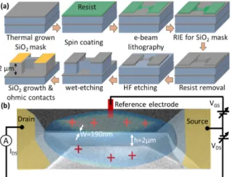
observed in the output response of the FinFET. The method presented here is promising for the development of reliable bio‐FETs as it can be extended to subsequent biomolecule immobilization steps to have a quality check of the surface functionalization process and to implement necessary further modifications. 2. Materials and Methods 2.1. FinFETs Fabrication The fabrication of Si FinFETs was reported in our previous work by Rollo et al. [19], as summarized in Figure 1a. The FinFETs were fabricated using anisotropic wet‐etching on p‐type Silicon on insulator (SOI) (Ultrasil Corporation, Hayward, CA, US) having a 2.2
± 0.1 μm thick silicon device layer (<110> oriented) with conductivity of 0.115 Ω∙cm
(equivalent doping ~ 1017 cm−3) and a 1 μm thick buried SiO2. The wafers were diced into
1 × 1 cm2 chips. A 50 nm layer of SiO2 was grown on top of the Si device layer by thermal
oxidation performed at 1050 °C in O2 environment (200 sccm) for 300 s. The devices in this
work were patterned using electron‐beam (e‐beam) lithography by first spin‐coating the
resist over the SOI chips and exposing them on an adapted electron microscope (FEI
Helios). However, we have also shown that these devices can be made using optical
lithography, thus they can be accessible to labs with no facilities for direct
nanolithography [21]. We used the FinFET design with a <110> crystallographic
orientation along the longitudinal axis of the FinFET, that was transferred onto the
underlying oxide using reactive ion etching process. Following the lithography, a short hydrofluoric acid etching step was carried out to remove the unwanted oxide outside the masked regions obtaining a smooth Si surface prior to the process of anisotropic etching.
A water solution of 25% tetramethylammonium hydroxide (TMAH) with 8.5% vol.
isopropanol was used to etch the Si device layer anisotropically obtaining vertical walls
on the FinFET sensing regions. A 20 nm layer of SiO2 was thermally grown over the
leads were defined using mask‐less laser lithography and e‐beam evaporation. The contacts and the chip surface were passivated using an SU8 epoxy layer leaving open the FinFET region. For the measurements in liquid, the chips were wire bonded on home‐ designed printed circuit boards and encapsulated using medical‐grade epoxy.
Figure 1. (a) Schematics of the process flow for the fabrication of Si Fin‐field effect transistors
(FETs). Silicon, SiO2, e‐beam sensitive resist, and ohmic contacts are represented in light blue,
grey, green and yellow, respectively. (b) Schematics illustrating operation of Si FinFET in liquid
gate configuration. 2.2. Chemical Modification of FinFETs and SPR Sensors: Vapor‐Phase APTES Silanization The chemical modification of the FinFET devices started with surface activation of the hydroxyl groups on the sensing SiO2 surfaces by low ozone exposing the chips into an UV lamp chamber for 5 min. Immediately after, the silanization process was carried out at a low‐pressure atmosphere (p = 1 × 10⁻³ mBar) inside a desiccator where small volumes (1–2 mL) of APTES were placed in a glass vial along with the FinFET chips (as shown in Figure 2a). The silanization process was carried out for 2.5 h at room temperature. After the functionalization, the chips were thoroughly rinsed with isopropanol to remove any
excess silane molecules and blow dried with nitrogen. The silanization protocol was
simultaneously implemented on SPR sensor chips to have a similar density of APTES
molecules (Figure 2b).
Figure 2. (a) Schematic representation of the Fin‐FET surface before and after the vapor‐phase 3‐
aminopropyltriethoxysilane (APTES) silanization. (b) Schematics illustrating the chemically
exploring the APTES functionalization. (c) Full SPR reflectance before (in black) and after the
APTES silanization process (in red) at λ = 785 nm. The inset shows the shift in SPR angular peak
minimum (ΘSPR).
2.3. pH Measurements Using FinFETs
The encapsulated FinFET chips were operated in liquid gate configuration using an
external reference electrode (DriRef‐2 Ag/AgCl from WPI) in buffers consisting of a
mixture of KH2PO4, citric and boric acids at 0.1 M all, mixed in equal volumes with 0.1 M KNO3 solution. For the pH‐sensing measurements with FinFETs, the pH of the prepared buffer solution was varied in the range of 3 to 11 by adding required volumes of 0.1 M KOH. A Keithley 2614HB DC source meter was used to apply the voltage to the source and drain and the reference electrode. To characterize multiple FinFETs in sequence, a multiplexer Keithley 3706A System Switch/Multimeter connected to a switching box was used. The devices were characterized before and after APTES functionalization. 2.4. MP‐SPR Measurements MP‐SPR measurements were performed using an SPR model Navi 220ATM (BioNavis Ltd., Tampere, Finland) setup. The SPR setup used two incident laser wavelengths, 670 and 785 nm, inlet and outlet (waste) tubings, and two independent flow channels. We used SPR sensor chips with a thin layer of SiO2 above the gold layer (from BioNavis Ltd.) for the APTES silanization to have binding reactions like the FinFET sensor surface. The temperature was kept at 20 °C and the measurements were carried out in Milli‐Q water.
SPR allows measuring the layer thickness even with submonolayer sensitivity
following the changes in refractive index of the layers in contact with the SPR sensor chips
detected as changes in the angle of minimum reflectivity (ΘSPR). MP‐SPR uses more than
one wavelength in combination with the scanning angle to obtain the layer thickness,
refractive indices, and surface mass densities [22,23]. Figure 2b illustrates the different
layers on the SPR sensor chips, and a thin layer of SiO2 above the gold (Au) layer was used
to adapt for the APTES silanization to yield binding reactions equivalent to the ones
occurring during FinFET functionalization. We evaluated the layer thickness (d) and
refractive index (n) for APTES molecules bound on sensor surface using the SPR Navi
LayerSolver v. 1.4 (BioNavis Ltd., Tampere, Finland) software using the full SPR angular reflectance measured at two wavelengths (670 and 785 nm), at the same point of time. The LayerSolver software creates a model of the different layers on the sensor chip to match
the full reflectance on the SPR sensor chip to adjust the change of ΘSPR at the two
wavelengths fitting the refractive index (n) and thickness (d) corresponding to the APTES layer using Fresnel refraction laws (the details are shown in Supplementary information). The obtained n and d are then connected to the mass surface concentration of adsorbed APTES (Γ) by de Feijter model that assumes that the refractive index is a linear function of the concentration (C) over a wide range of concentrations: 𝛤 𝑑 𝑛𝑑𝑛 𝑛 𝑑𝐶 (1) where n0 is the medium refractive index and dn/dC is a coefficient known as refractive
index increment, which is the derivative of the refractive index with respect to the
molecule concentration in solution. When dn/dC is not available from experimental data, it can be also estimated from the physicochemical properties of APTES, in particular from the volumetrical density ν and the refractive indexes from the solvent and APTES [24]: 𝑑𝑛 𝑑𝐶 3 2𝑛 𝜈 𝑛 𝑛 𝑛 2𝑛 (2)
3. Results
We deployed MP‐SPR to evaluate the thickness and molecular density of the APTES
layer deposited via vapor‐phase silanization. Figure 2c shows an exemplary measurement
taken at λ = 785 nm before (black curve) and after the APTES silanization (red curve) also
zoomed in the inset. As shown, on binding of APTES molecules at the SPR chip, ΘSPR shifts
towards larger angles [20]. We obtained the thickness and refractive index of APTES layer
as d = 1.7 nm and n = 1.41. Parallel to the chip functionalisation on the FinFETs, we
introduced a chip SiO2/Si that was grown in the same process as our devices. The thickness
measured by SPR was comparable to the values obtained from ellipsometry (d = 1.9 ± 0.2
nm) carried out on APTES‐coated SiO2/Si chips (details in supplementary material and
was higher than the APTES monolayer thickness reported in literature (~1 nm) [25]. As
the thickness and refractive index measured via SPR gives an average over the entire
sensor surface, we assumed that the higher thickness of APTES layer could be due to
partial agglomerates that formed on the sensor surface during the vapour‐phase
silanization process. We used the specific volume value of APTES from the literature and Equation (1) to evaluate the surface coverage of APTES molecules at the sensor surface
(Ns) as 4.45 × 10¹⁸ molecules/m2. As we do not have a way to determine the distribution of
agglomerates, we assumed this number as the number of APTES group present on the sensor for our modelling to calculate the sensitivity of the ISFETs.
3.1. Modification of the pH Sensitivity of the Surface Potential with APTES
The experiments for pH sensing were carried out in three devices using a liquid gate
configuration as shown in Figure 1b. The working ranges of these devices were
characterized in our previous work [19]. We characterized the changes in surface potential
due to the chemical modification of the FinFETs following the VGS at fixed IDS with
different pH buffers (in a range from 11 to 3), measured before and after APTES
functionalization.
Figure 3 reports the results of VGS versus ISD from a representative FinFET at different pHs
(3, 5, 7, 8, 10) before and after APTES silanization. For these measurements, VDS was fixed at 300 mV. The dimensions of this device (hereby designed as device 1) characterized by SEM microscopy were 190 nm, 14, and 2 μm for width, length and height, respectively. We compared the changes of VGS with pH on two other devices of the same batch hereby designated devices 2 and 3, which had bigger widths of 300 and 320 nm, respectively. In all devices we observed that the IDS transfer characteristics shifted towards more positive VGS values with more alkaline solutions due to the effect of the adsorbed charges on the majority charge carriers within the channel (holes in our case), as illustrated on Figure 3a
with the data from device 1 having the smallest width. At higher pH values there are
fewer protons in the solution and therefore the equilibrium with the surface chemical
groups promotes deprotonation, resulting in the negatively charged oxide. This change in
the surface potential (ψ0) influences the hole carriers within the FinFET channel, causing
the need for the modulation of the electrolyte potential (ΔVGS = −Δψ0) to keep the current
constant through the channel. VGS vs pH extracted at constant IDS = 2.25 μA before (black
solid squares) and after the APTES silanization (red open circles) is shown as a scatter plot
in Figure 3b. We calculated the average sensitivity of the oxide surface (ΔVGS/ΔpH) before
and after APTES silanization process from a linear fit in Figure 3b. The ΔVGS/ΔpH of bare
SiO2 was 31 ± 1 mV/pH with a relatively non‐linear response calculated by the coefficient
of the determination R‐squared (Rsq) calculated from the fitting Rsq = 0.988. The sensitivity
value is comparable to the values that we obtained in similar devices where we used the same oxidation process [21]. As expected, the values that deviated most from the linear behavior were the values at the most acidic pH’s. The non‐linearity in the pH response for SiO2‐based dielectrics has been previously explained in literature and is linked to the low the protonation affinity of silanol groups (pKb ≈ −2) that makes the proton dissociation the only process associated to the charging of the surface [16]. A relatively higher linearity
with Rsq = 0.996 and average ΔVGS/ΔpH = 36 ± 1 mV/pH was observed for the APTES functionalized surfaces. This was a modest improvement, but it was consistent with other works in literature [17,18]. As APTES has a double charging mechanism corresponding to
the active protonation and deprotonation of amino groups that have pKa and pKb of 9 [17]
and 3.63 [26], respectively, the increase linearity was expected. Also, the narrower gap
between pKa and pKb contribute to the higher sensitivity.
Figure 3. (a) Transfer IDS vs. VGS of a FinFET before (top) and after the APTES silanization process (bottom) with different pH (3, 5, 7, 8, 10) shown in different colors. (b) Scatter plot of VGS vs. pH before (black squares) and after the APTES silanization process (red open circles). The ΔVGS/ΔpH evaluated from the linear fit of the plots are indicated in the inset. For these measurements VDS was fixed at 300 mV. 3.2. Chemical Characterisation of the Surface Properties Using the Buffering Capacity Determined from the Surface Potential To get a better insight on the properties of the current APTES functionalization we compared experimental results with a site binding model of the dielectric surface. The relation between the changes in the surface potential (ψ0) with the pH of the bulk solution
are compensated by VGS (ΔVGS = −Δψ0). The sensitivity of ISFETs for ψ0 is well described in
literature [16] with a Nernstian framework:
∆𝜓
∆𝑝𝐻 2.303
𝑘𝑇
𝑞 𝛼 (3)
where k, T and q are the Boltzmann constant, absolute temperature and elementary charge,
respectively. α is a dimensionless sensitivity parameter between 0 and 1 determined by the electrostatic interactions at the surface of the dielectric and distribution of ions inside the electrolyte, and is given by [16]: 𝛼 1 1 2.3𝑘𝑇𝐶𝑞 𝛽 (4)
where Cdiff is the differential capacitance of the electrical double layer that depends upon
the properties of electrolyte solution. The intrinsic buffer capacity (βint) gives the measure
of charging capability of the oxide surface with changes in pH of the buffer solution. It
depends on the intrinsic properties of the oxide surface and changes every time a chemical
group contributes to the charging and un‐charging of the sensor interface. In a FET device,
for low Cdiff, and high βint, α will be close to 1 and thus maximum pH sensitivity can be
obtained. For Cdiff and βint we used a site binding model combined with a Stern
Gouy–Chapman approximation (CGCh) with an estimation of the stern layer (CStern = 0.8 F) considered as the two capacitances in series: 𝐶 𝐶 ∙ 𝐶 𝐶 𝐶 (5) and with CGCh is: 𝐶 2𝑧 𝑞 𝜀𝜀 𝐼 𝑘𝑇 𝑐𝑜𝑠ℎ 𝑧𝑞𝜓 2𝑘𝑇 (6)
where z is the coordination number of the ions (one in the case of protons), ε0 is the
dielectric constant of vacuum, ε is the relative dielectric constant of the medium (water in
our case), and I is the number concentration of the ions in the bulk. βint in the site‐binding
model depends upon the different dissociation constants and the density of binding sites:
𝛽 𝑁 𝐾 𝑎 4𝐾 𝐾 𝑎 𝐾 𝑘
𝐾 𝐾 𝐾 𝑎 𝑎
2.3𝑎 (7)
where Ki are the different dissociation constants and 𝑎 is the proton activity at the
surface of the liquid interface, which is related to the bulk 𝑎 as: 𝑎 𝑎 𝑒𝑥𝑝 𝑞𝜓 𝑘𝑇 (8) or equivalently: 𝑝𝐻 𝑝𝐻 𝑞𝜓 2.3 𝑘𝑇 (9) where the origin of ψ0 is chosen at the point of zero charge. Combining equations 3–6 it is
also possible to extract an experimental βint and compare it with the site binding model
where the Ns used is the one calculated with our SPR results. In this model we used the
values of VGS to calculate ψ0 using the following relation:
𝜓 𝑝𝐻 𝑉 𝑝𝐻 𝑉 𝑝𝐻 (10)
where pHpzc is the pH value at the point of zero charge (pHpzc= pKa + pKb)/2). The exact value
of VGS(pHPZC) was extracted from the linear fit of the experimental VGS(pH).
Figure 4 shows the comparison of the experimental and the model βint with changing
pH for all the devices (model and experimental βint are represented with black solid signs
and red open signs, respectively, while device 1 to 3 are represented with squares, circles
and triangles, respectively). The model of βint for APTES shows how the number of active
sites that provide buffering capacitance increase for the values of pH lower and higher
than ~3.63 and ~9, respectively, corresponding to the APTES dissociation constants for pKb
and pKa, respectively. The experimental βint also follows that behavior, but there is also an
increase of the buffering sites at pH slightly higher than 7.5. This could be attributed also to contaminants or defects in the functionalization, that would contribute with charges,
for example, from uncovered silanol groups (that have pKa at 6). However, the differences
between the experimental βint all three devices showed the same behavior that we interpret
as a similar functionalization achieved on the three sensors, which we attribute to the large
surface area of all devices.
The behavior of the experimental βint, shown in red in Figure 4, having increasing
buffering capacitance at more than one pH value, is also a chemical fingerprint of the
APTES functionalization. This behavior is opposed to the SiO2 where βint has only one
maximum attributed to the single protonation of silanol groups (the comparison of the
Figure 4. Comparison between modelled (in black) and experimental (in red) intrinsic buffering
capacitance of the APTES functionalized surface as obtained for the three devices 1 to 3
represented with squares, circles and triangles, respectively.
3.3. Preservation of Linear Response by the FinFETs in the Output Characteristics
For multiplexed systems, it is also important to consider that measuring the output currents may be more convenient than following the surface potential with the reference electrode, which in most configurations will be common to all devices [20]. Previously,
we showed that the high aspect ratio of FinFETs provides a more linear ΔIDS/ΔpH
response in comparison to Si NW‐based FETs [19], while the double side gating would
provide a sensitivity advantage to the FinFETs with respect to planar NWs. Figure 5a
shows Ids vs Vds at different pH buffer solutions (3, 5, 7, 8, 10), before and after APTES
silanization. For these experiments we connected directly the source with the gate voltage
(VGS = 0). The conductance of the devices increased with increasing pH of the buffer
solution due to the effect of the proton concentration on the majority charge carriers as described earlier. We evaluated the conductance of the FinFET devices at different buffer
pH values before and after APTES silanization from the linear fitting of the output
characteristics. The conductance of the devices increased with increase in pH of the buffer solution and is shown as a scatter plot before (black solid squares) and after silanization
(red open circles) in Figure 5b. We observed a small bump around 15 mV, which we
attribute to defects on the contacts, nevertheless the curves were symmetric and the IDS vs
VDS pass through zero, so we considered our devices Ohmic in the studied range. On linear fitting of the conductance plots shown as black and red lines in Figure 5b, we obtained average change in conductance of the devices as 158 ± 9 nS/pH and 176 ± 6 mS/pH per unit area before and after APTES silanization, respectively. We attribute the increase in conductance change of the devices to the changes in the density of pH sensitive groups at
the oxide surface as described earlier. Moreover, the increased linear response in
conductance change on APTES silanization is in accordance with the linearity increment observed in the surface potential changes.
Figure 5. (a) Output characteristics of the FinFET device 1 measured before and after the APTES
silanization process at different buffer pH values (3, 5, 7, 8, 10) shown in different colors (blue, red,
green pink and light blue, respectively). (b) Scatter plot showing the variation of conductance (G)
in the FinFET, evaluated from the output characteristics as a function of buffer pH (varied from 3
to 11) before (black squares) and after the silanization process (red open circles). The linear fits of
the scatter plots are shown as black and red lines for before and after APTES silanization,
respectively. The average conductance change (ΔG/ΔpH) is also shown in the inset. For these
experiments VGS = 0.
4. Conclusions
In this work we have presented a high height‐to‐width aspect ratio FinFET chemical
sensor with a surface modification of the dielectric barrier using APTES coatings. We used
a vapor‐phase silanization method made in a home‐built setup to obtain a well‐defined
thickness of APTES molecules linked covalently at the SiO2 sensing surface of the FinFETs.
We tested the sensitivity of the FinFET devices before and after chemical modification
with APTES in a buffer pH range of 3 to 11. ΔVGS/ΔpH improved from 31 mV/pH
measured on the devices with SiO2 to 36 mV/pH with APTES. In addition to the increment
in the sensitivity of the FinFET devices, the linearity in the pH response also improved
with APTES functionalization. The output response of the chemically modified high‐
aspect ratio FinFETs also showed an improvement in linearity and conductance change
(ΔG/ΔpH). We attribute the enhanced pH sensitivity and response linearity of the
chemically modified FinFET devices to the presence of amine groups at the sensing oxide, which can create charges both with protonation and deprotonation mechanisms.
The improvements we obtained were modest, probably because our starting surface
was not optimum for the growth of the SiO2 and we could not use a dedicated reactor.
Some authors followed the functionalization following the increase of thickness by
ellipsometry [18], or with AFM measurements. We could not use AFM due to the high
aspect ratio of the FinFETs, but we followed the formation of APTES layers with
ellipsometry in a SiO2 substrate deposited in parallel with our wires, and in an SPR chip.
We analyzed the contribution of the buffering capacitance of the different reactive groups
at the sensing oxide surface that influenced the proton sensitivity of the chemically
modified FinFET devices. We compared the βint evaluated from a site binding model and
experimentally derived using a Stern–Gouy–Chapman approximation for the differential
capacitance. The comparison of the experimental data with a model considering only
amine groups showed the existence of a contribution compatible with the presence of
unoccupied silanol sites. This contribution suggests also that the distribution of APTES
was not completely homogeneous, and that pockets and small aggregates may have
occurred in the functionalization. Thus, the βint evaluated from the experimental data is
also a fingerprint of the functionalization.
In conclusion, chemical modification (with APTES) of high‐aspect‐ratio FinFETs
which are intrinsically advantageous due to their improved linearity in transduction
terms of sensitivity and linearity that is desired for bio‐chemical sensors. High‐aspect‐ ratio FinFETs provide higher currents than NWs by a factor proportional to the height‐to‐ width aspect ratio. The high‐aspect‐ratio FinFETs keep many of the advantages of Si NWs
regarding the more efficient gating and smaller footprints, while incorporating other
advantages typical of planar sensors, as there is a larger planar surface area available for functionalization and a conduction channel less sensitive to defects. Also, they offer direct
gating which is not contaminated by parasitic capacitance during gate coupling, as
compared to extended gate configurations. Regardless, the modest improvement in
sensitivity by APTES has shown in the literature to improve the stability of SiO2 and to be
a good tethering point for peptide bond functionalization. Thus, the APTES‐
functionalized FinFETs are promising both for pH sensing and for the development of
biosensors using the amine sites as tethering groups for the functionalization of other
receptor molecules.
Supplementary Materials: The following are available online at www.mdpi.com/2227‐
9040/9/2/20/s1, Figure S1: Full SPR spectra after APTES silanization of the SPR sensor chips at two
wavelengths, 670 and 785 nm, illustrating good alignment between the measured and the modeled
data. The measured spectra are shown in light blue and red colors while the modeled one as dark
blue and brown colors, Figure S2: SEM pictures and the corresponding Ids vs Vds pH curves from
devices 1 to 3, Figure S3: Plot showing the variation of VGS change extracted from the transfer
characteristics as a function of buffer pH for 3 FinFETs (Ch1, 2,3) measured before (SiO2) and after
the APTES silanization. The VGS change was extracted by subtracting the VGS values obtained after
fixing the IDS, at each buffer pH value with respect to the value at pH 3, Figure S4: comparison
between the buffering capacitance of SiO2 (a) and the APTES functionalised surface in device 1.
Author Contributions: Conceptualization, C.P.G. and W.O.; methodology, C.P.G., S.K.; validation,
C.P.G. and S.K.; formal analysis, C.P.G. and D.R.; investigation, C.P.G. and D.R.; resources, C.P.G.
and S.K.; data curation, C.P.G., D.R. and S.R.; writing—original draft preparation, C.P.G. and D.R.;
writing—review and editing All; supervision, C.P.G., S.K.; project administration, C.P.G., S.K.;
funding acquisition C.P.G., S.K. All authors have read and agreed to the published version of the
manuscript.
Funding: This work was financed by the H2020 program in the project ELECTROMED in the
framework of the FET‐OPEN Action (Grant agreement ID: 862539) and by the Luxembourg National
Fund (FNR) with the projects NANOpH (grant 5718158) under the Attract program and PLASENS
(grant CM15/MS/10459961) under the CORE program.
Institutional Review Board Statement: Not applicable.
Informed Consent Statement: Not applicable.
Data Availability Statement: The data presented in this study are available on request from the
corresponding author.
Conflicts of Interest: The authors declare no conflict of interest.
References
1. Bergveld, P. Thirty years of ISFETOLOGY: What happened in the past 30 years and what may happen in the next 30 years.
Sensors Actuators B Chem. 2003, 88, 1–20, doi:10.1016/S0925‐4005(02)00301‐5.
2. Syu, Y.‐C.; Hsu, W.‐E.; Lin, C.‐T. Review—Field‐Effect Transistor Biosensing: Devices and Clinical Applications. ECS J. Solid
State Sci. Technol. 2018, 7, Q3196–Q3207, doi:10.1149/2.0291807jss.
3. Bergveld, P. Development of an Ion‐Sensitive Solid‐State Device for Neurophysiological Measurements. IEEE Trans. Biomed. Eng. 1970, 1, 70–71. Available Online: https://ieeexplore‐ieee‐org.proxy.bnl.lu/stamp/stamp.jsp?tp=&arnumber=4502688
(accessed on 19 January 2021).
4. Rothberg, J.M.; Hinz, W.; Rearick, T.M.; Schultz, J.; Mileski, W.; Davey, M.; Leamon, J.H.; Johnson, K.; Milgrew, M.J.; Edwards,
M.; et al. An integrated semiconductor device enabling non‐optical genome sequencing. Nature 2011, 475, 348–352,
doi:10.1038/nature10242.
5. Merriman, B.; Torrent, I.; Rothberg, J.M. Progress in Ion Torrent semiconductor chip based sequencing. Electrophoresis 2012, 33,
6. Moser, N.; Keeble, L.; Rodriguez‐Manzano, J.; Georgiou, P. ISFET arrays for lab‐on‐chip technology: A review. In Proceedings
of the 2019 26th IEEE International Conference on Electronics, Circuits and Systems (ICECS), Genoa, Italy, 27–29 November
2019; pp. 57–60, doi:10.1109/ICECS46596.2019.8965034.
7. Moser, N.; Lande, T.S.; Toumazou, C.; Georgiou, P. ISFETs in CMOS and Emergent Trends in Instrumentation: A Review. IEEE
Sens. J. 2016, 16, 6496–6514, doi:10.1109/JSEN.2016.2585920.
8. Kaisti, M. Detection principles of biological and chemical FET sensors. Biosens. Bioelectron. 2017, 98, 437–448.
9. Cai, J.; Ning, T.H.; Yau, J.‐B.; Zafar, S. Charge sensors using inverted lateral bipolar junction transistors. Google Patents, US
8,980,667 B2, 17 March 2015.
10. Zaborowski, M.; Tomaszewski, D.; Dumania, P.; Grabiec, P. From FinFET to nanowire ISFET. In Proceedings of the European
Solid‐State Device Research Conference (ESSDERC), Bordeaux, France, 17–21 September, 2012; pp. 165–168,
doi:10.1109/ESSDERC.2012.6343359.
11. Nair, P.R.; Alam, M.A. Performance limits of nanobiosensors. Appl. Phys. Lett. 2006, 88, 9–11, doi:10.1063/1.2211310.
12. Chen, S.; Van Den Berg, A.; Carlen, E.T. Sensitivity and detection limit analysis of silicon nanowire bio(chemical) sensors.
Sensors Actuators B Chem. 2015, 209, 486–489, doi:10.1016/j.snb.2014.12.007.
13. Chen, S. Silicon Nanowire Field‐Effect Chemical Sensor, Wohrmann Print Service, Zutphen, the Netherlands, 2011; Vol. 4, pp. 915– 919.
14. Rollo, S.; Rani, D.; Olthuis, W.; García, C.P. Single step fabrication of Silicon resistors on SOI substrate used as Thermistors. Sci. Rep. 2019, 9, 1–7, doi:10.1038/s41598‐019‐38753‐x.
15. Topkar, A.; Lal, R. Effect of electrolyte exposure on silicon dioxide in electrolyte‐oxide‐semiconductor structures. Thin Solid
Films 1993, 232, 265–270, doi:10.1016/0040‐6090(93)90020‐P.
16. Van Hal, R.E.G.; Eijkel, J.C.T.; Bergveld, P. A general model to describe the electrostatic potential at electrolyte oxide interfaces.
Adv. Colloid Interface Sci. 1996, 69, 31–62.
17. Chen, S.; Bomer, J.G.; Carlen, E.T.; Van Den Berg, A. Al2O3/silicon nanoISFET with near ideal nernstian response. Nano Lett.
2011, 11, 2334–2341, doi:10.1021/nl200623n.
18. Liang, Y.; Huang, J.; Zang, P.; Kim, J.; Hu, W. Molecular layer deposition of APTES on silicon nanowire biosensors: Surface
characterization, stability and pH response. Appl. Surf. Sci. 2014, 322, 202–208.
19. Rollo, S.; Rani, D.; Leturcq, R.; Olthuis, W.; García, C.P. High Aspect Ratio Fin‐Ion Sensitive Field Effect Transistor:
Compromises toward Better Electrochemical Biosensing. Nano Lett. 2019, doi:10.1021/acs.nanolett.8b04988.
20. Miscourides, N.; Georgiou, P. ISFET arrays in CMOS: A head‐to‐head comparison between voltage and current mode. IEEE
Sens. J. 2019, 19, 1224–1238, doi:10.1109/JSEN.2018.2881499.
21. Rollo, S.; Rani, D.; Olthuis, W.; García, C.P. High performance Fin‐FET electrochemical sensor with high‐k dielectric materials.
Sensors Actuators B Chem. 2020, 303, 127215.
22. Granqvist, N.; Liang, H.; Laurila, T.; Sadowski, J.; Yliperttula, M.; Viitala, T. Characterizing ultrathin and thick organic layers
by surface plasmon resonance three‐wavelength and waveguide mode analysis. Langmuir 2013, 29, 8561–8571.
23. Kari, O.K.; Rojalin, T.; Salmaso, S.; Barattin, M.; Jarva, H.; Meri, S.; Yliperttula, M.; Viitala, T.; Urtti, A. Multi‐parametric surface
plasmon resonance platform for studying liposome‐serum interactions and protein corona formation. Drug Deliv. Transl. Res.
2017, 7, 228–240.
24. Zhao, H.; Brown, P.H.; Schuck, P. On the distribution of protein refractive index increments. Biophys. J. 2011, 100, 2309–2317,
doi:10.1016/j.bpj.2011.03.004.
25. Munief, W.M.; Heib, F.; Hempel, F.; Lu, X.; Schwartz, M.; Pachauri, V.; Hempelmann, R.; Schmitt, M.; Ingebrandt, S. Silane
deposition via gas‐phase evaporation and high‐resolution surface characterization of the ultrathin siloxane coatings. Langmuir
2018, 34, 10217–10229.
26. Extracted from Chemical Properties of 3‐Aminopropyltriethoxysilane; Available Online:
https://www.chemicalbook.com/ProductMSDSDetailCB8686147_EN.htm (accessed on 19 January 2021).