RTOS CONTROL OF HARDWARE PROCESSES
SUMAIA ATIWA
A THESIS SUBMITTED TO THE FACULTY OF GRADUATE STUDIES IN PARTIAL FULFILMENT OF THE REQUIREMENTS
FOR THE DEGREE OF MASTER OF APPLIED SCIENCE
GRADUATE PROGRAM IN ELECTRICAL ENGINEERING AND COMPUTER SCIENCE YORK UNIVERSITY TORONTO, ONTARIO DECEMBER 2016 c SUMAIA ATIWA, 2016
Abstract
In this thesis, adding hardware-process support to Microcontroller Real-time Operating System Version 2 (MicroC/OS-II) is proposed. µC/OS-II is a hard real-time operating system (RTOS), mostly written in the C programming language. µC/OS-II is designed to manage limited resources within embedded systems, and it can only execute and control software processes performed in the same processor system. µC/OS-II has been modified in order to manage external hardware processes. These hardware processes are imple-mented on a Nexys 3 Spartan-6 FPGA Board. In this thesis,µC/OS-II is already ported to run on an EVBplus HCS12 development board with CodeWarrior Embedded Soft-ware Development Tools from Freescale Semiconductor Inc. Modifications are applied on µC/OS-II interrupt system to manage hardware processes, and SPI protocol and parallel interface are set up to communicate between the HCS12 trainer and the FPGA board. The work is illustrated by designing a satellite attitude controller, using variable structure control (VSC).
Acknowledgements
I cannot find the words to express my gratitude to my supervisor Professor Mokhtar Aboelaze for his expert supervision. He has been extremely helpful since I started my degree. Ever since, Dr. Mokhtar has supported me not only by providing a research assistantship over more than two years, but also academically and emotionally through the rough road to finishing this thesis. I highly appreciate the valuable advice, professional guidance, and consistent encouragement from Professor Mokhtar Aboelaze in all the stages of my study and research.
I am also grateful to my thesis committee members, Professors Ahmed Eldyasti and Suprakash Datta, for reviewing my thesis and providing their valuable insights.
I would like to dedicate this thesis to my family and my friends for their deepest love, utmost encouragement, and unconditional support.
Table of Contents
Abstract ii
Acknowledgements iii
Table of Contents iv
List of Tables vii
List of Figures viii
1 Introduction 1
1.1 Overview of a Real-Time Operating System . . . 2
1.2 Types of Real-Time Operating Systems . . . 3
1.3 Field Programmable Gate Array (FPGA) Technology . . . 5
1.4 Motivations and Contributions of the Thesis . . . 6
1.5 Thesis Organization . . . 8
2.1 Operating Systems for FPGAs . . . 10
2.2 RTOS Implementation in Hardware . . . 11
2.3 Chapter Summary . . . 14
3 Hardware Review 15 3.1 Overview of EVBplus HCS12 Development Board . . . 15
3.2 Overview of FPGA Technology . . . 17
3.2.1 FPGA Design Flow . . . 21
3.3 Chapter Summary . . . 23 4 MicroC/OS-II 24 4.1 Overview of MicroC/OS-II . . . 24 4.2 Functions of MicroC/OS-II . . . 27 4.2.1 Task management . . . 27 4.2.2 Time management . . . 29
4.2.3 Inter-task communication and synchronization . . . 29
4.2.4 Fixed size Memory management . . . 33
4.2.5 Interrupts and ISR . . . 33
4.3 Chapter Summary . . . 34
5 Implementaion 35 5.1 Overview of Serial Peripheral Interface (SPI) . . . 35
5.3 FPGA implementation of SPI Slave . . . 40
5.4 Chapter Summary . . . 42
6 Design Example: Satellite Attitude Controller 43 6.1 Overview of Satellite Attitude Control . . . 44
6.2 Hardware in The Loop (HiL) . . . 44
6.3 Variable Structure Control (VSC) . . . 45
6.4 Implementation of a Satellite Attitude Control system . . . 46
6.4.1 Model Implementation . . . 50
6.4.2 Controller Implementation . . . 55
6.4.3 Fixed Point . . . 57
6.4.4 Discussion and Observations . . . 61
6.5 Chapter Summary . . . 63
7 Conclusion and Future Research Directions 64
List of Tables
5.1 SPI Specifications . . . 37 5.2 Synthesis Summary of SPI Slave . . . 42
List of Figures
3.1 FPGA Architecture . . . 19
3.2 Nexys 3 Spartan-6 FPGA Trainer Board [18] . . . 20
3.3 FPGA Design Flow . . . 22
4.1 MicroC/OS-II Architecture . . . 26 4.2 Task States . . . 29 4.3 Event Flags . . . 31 4.4 Semaphores . . . 31 4.5 Message Mailboxes . . . 32 4.6 Message Queues . . . 32 5.1 SPI Architecture . . . 36
5.2 RTL Schematic of SPI Slave . . . 41
5.3 The final design . . . 41
6.2 Block diagram of the satellite model . . . 54 6.3 Floating point and fixed point response forθ1 . . . 59
Chapter 1
Introduction
The objective of this research is to add hardware-process support to an RTOS. In many commercial real-time operating systems such asµC/OS-II and VxWorks, there is no run-time support to handle hardware processes executed on reconfigurable fabrics such as Field Programmable Gate Array (FPGA) devices. Due to the proliferation of FPGA technology in real-time applications, there is a need to integrate both software and hard-ware processes.
In this chapter, section 1.1 provides an overview of real-time operating systems, and RTOS categories are described next in section 1.2. Section 1.3 briefly reviews FPGA technologies. Section 1.4 presents the motivations and contributions of the thesis. In the section 1.5, the outline of the thesis is provided.
1.1 Overview of a Real-Time Operating System
A real-time operating system (RTOS) is an operating system that handles one or more dedicated, preprogrammed functions, using limited resources and subject to real-time constraints [5, 37]. Real-time operating systems are developed taking into consideration characteristics such as portability, scalability, memory usage and power consumption to meet the needs of embedded systems [47]. An embedded system refers to an electronic or mechanical system that contains a built-in microprocessor or microcontroller, dedicated for a specific application [20, 27]. Embedded systems are designed to meet limited re-sources in terms of development cost, power and memory, and they are classified into two categories: hard and soft. In hard real-time systems, missing deadlines to produce system outcomes can lead to fatal or dangerous consequences, whereas in soft real-time systems, deadlines misses can be tolerable, but they may degrade the system performance.
A task is defined as a software, independent and asynchronous activity run and con-trolled by an RTOS. An RTOS kernel is mainly responsible for task dispatching, schedul-ing and inter-task communication. In sschedul-ingle, sequential processor systems, only one task is performed at any given time, while multi-core processor systems can schedule more than one task simultaneously. Thus, the scheduler portion of the RTOS kernel uses scheduling algorithms such as round-robin and priority, pre-emptive scheduling to simultaneously manage multiple tasks.
1.2 Types of Real-Time Operating Systems
According to the scheduling algorithm [5], RTOS systems can be categorized into:
• Polled Loop Systems
• Polled Loop with Interrupts
• Round-Robin Systems
• Preemptive Priority Multitasking Systems
(1) Polled Loop Systems
A polled Loop kernel is the simplest real-time kernel to write, debug and implement. Only polling method is used to scan input devices in order to determine which task requires the microprocessor time. This kernel is preferable when all tasks have an equal priority. Once a task starts, it runs to completion. Therefore, it is easy to determine the response time of a task, and no inter-task communication is needed in these systems. Nonetheless, this RTOS is not suitable for complicated applications where multiple tasks have to be handled simultaneously. Furthermore, no interrupts can be handled from hardware devices in this style of programming. Thus, I/O devices must be polled as frequently as necessary, so that critical events are unlikely to be missed. However, polling a device leads to unnecessarily wasting energy.
(2) Polled Loop with Interrupts
This RTOS is also referred to as a foreground/background system. Both a polling algorithm and interrupt are used to maintain regular events and asynchronous, time-sensitive events respectively. This system performs a regular event as an infinite loop called a task, whereas critical events are executed by serving Interrupt Service Routines (ISRs). A task level is the background system, and it is first implemented and tested. After that, the interrupt system is designed and added to the first stage, which is called foreground.
(3) Round-Robin Systems
Similar to the previous system, software designers organize the system’s functions into tasks, but polling is used to manage I/O devices’ events instead of interrupts. Every task is run from the beginning to completion, and then CPU control moves to the next task in a cyclical manner. If this scheduling kernel algorithm uses time-slicing techniques, each task can access the processor time for an equal time slice, and then the kernel sequences to another task in circular order until all tasks have been completely executed..
(4) Preemptive Priority Multitasking Systems
All previously mentioned kernels are called non-preemptive, because each task is run from the beginning to completion, without being preempted by other tasks. Unlike preemptive Priority multitasking systems, higher priority tasks can preempt
to each task, and examines the set of ready tasks to determine the highest priority task to run. The lower the priority number the higher the priority of a task. The priority can be fixed in compilation time and also be changed in runtime. µC/OS-II is a commercial example for preemptive priority multitasking systems used in the thesis and explained in Chapter 4.
1.3 Field Programmable Gate Array (FPGA) Technology
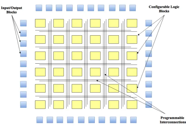
FPGA is a chip that a developer can change and update its logic functionality after it has been fabricated [6]. In fact, a FPGA chip is an array of configurable logic boxes (CLBs) connected by programmable interconnections, and it exchanges data and control signals with the external environment through I/O pins as demonstrated in figure 3.1. Each configurable logic box performs a logic function. The process of configuring an FPGA chip determines the functions of CLBs and the route of the programmable interconnections between these logic blocks.
FPGAs have become an attractive solution for implementing embedded systems be-cause this solution allows multiple system components to be implemented and integrated into a single chip [32]. Compared to microprocessors, FPGAs can consume less power because of their capability to work at lower frequencies, and FPGAs can provide much faster solutions due to their high parallelism feature. Furthermore, because FPGAs are manufactured with a reconfigurable functionality, they have fast time-to-market. With FPGA technologies, hardware designers can securely and conveniently write, customize,
debug and test their designs in their labs or even in-house after purchasing an FPGA board.
1.4 Motivations and Contributions of the Thesis
Real-time embedded operating systems have been widely used in many commercial prod-ucts such as digital cameras, cellular phones, medical devices, network adapters and ATM machines [5]. Nevertheless, many commercial real-time operating systems such as µC/OS-II and VxWorks do not provide run-time support to manage hardware processes run and executed on external hardware platforms [39]. Compared to software processes, the execution domain of hardware processes is different, in that they are executed on external hardware platforms such as FPGA fabrics instead of the processor system.
In many applications where speed and power are important consideration, special purpose hardware or accelerators are used [8]. Compared to CPUs, accelerators consume less power and operate faster. Hardware acceleration can be designed using FPGA or Application-specific Integrated Circuit (ASIC) technologies. For low volume applications, FPGAs are preferable in terms of time-to-market, Non Recurring Expenses s(NRE), de-sign cycle and reconfigurability. There is no layout or masks required in the manufacturing process for FPGA design, which speeds up time-to-market. NRE costs for FPGAs are less than ASICs. The FPGA design cycle is simpler because software tools are responsible for handling mapping, placement, routing and timing. Reconfiguration is the main feature of FPGAs, which is the capability of being reprogrammed an unlimited number of times to
implement any customized hardware circuit, while ASICs have fixed functionality after have been fabricated.
Adding hardware-process support to a real-time operation system allows RTOS users to compile and execute their hardware designs on FPGA fabrics as if they execute soft-ware programs on processor-based systems. This support includes creating, deleting and scheduling hardware processes, and inter-process communication and synchronization.
Our thesis work aims to implement support of hardware processes in real-time oper-ating systems namely,µC/OS-II using an FPGA-based hardware solution. This research area is relatively new, and very little work has been done. The thesis work includes adding software support in the RTOS, and implementing hardware processes and hard-ware interface on the FPGA board.
• First, Serial Peripheral Interface (SPI) protocol is established in hardware and soft-ware on the Nexys3 and Dragon12-Plus boards to allow these platforms to commu-nicate and exchange data and control signals.
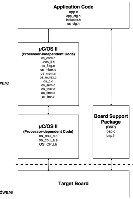
• Adding C and header files of the SPI and parallel interface to the board support package (BSP) file of theµC/OS-II as shown in figure 4.1
• After that, ISR is added to the board support package (BSP) file of theµC/OS-II to handle hardware processes performed on the FPGA board.
• Finally, hardware implementation of a satellite attitude control system using vari-able structure control (VSC) and the Hardware-in-the loop (HiL) emulator are
designed on the Nexys3 FPGA board, and power consumption and logic resources for the design of the satellite attitude controller are calculated for floating point and fixed-point representations.
1.5 Thesis Organization
The remaining of the thesis is organized into six chapters. First, Chapter 2 discusses a literature review of the previous work. Chapter 3 illustrates the EVBplus HCS12 development board and FPGA technologies. Chapter 4 demonstrates MicroC/OS-II and its functions. Chapter 5 describes the implementation process for the communication protocols between the Nexys3 and EVBpuls development boards. Chapter 6 introduces a satellite attitude controller as our thesis application. Chapter 7 pprovides the conclusion of the thesis and directions for future research.
Chapter 2
Related Work
Recently, FPGAs have become a key enabling technology in developing embedded systems due to their flexible configuration capabilities to implement any customized hardware circuit [11, 32]. In fact, FPGAs offer reasonable solutions in terms of development cost, power and performance for embedded systems. Therefore, it is essential to examine the issue of integrating software tasks, controlled by an RTOS running on a CPU system, with hardware processes running on an FPGA device. There has not been enough research on upgrading an RTOS to control external hardware processes, although some researchers have attempted to explore and demonstrate this issue using different approaches.
In this chapter, section 2.1 explores a few papers that introduced and proposed oper-ating systems for FPGAs. Section 2.2 provides examples for either partially or completely implementing RTOS in hardware. Section 2.3 summarizes the content of the chapter.
2.1 Operating Systems for FPGAs
Software specialists are unlikely to be knowledgeable about managing hardware mod-ules and logic resources built on FPGA platforms. To overcome this obstacle, several researchers have introduced operating systems for reconfigurable architectures on FPGA technologies. These operating systems are responsible for managing hardware tasks run-ning on reconfigurable fabrics, and their functionalities include task scheduling, data communication and synchronization.
Pellizzoni and Caccamo in [36] presented a resource allocation scheme and admission control test to manage hardware and software tasks running on a system-on-chip (SoC), namely a Xilinx Virtex-4 FPGA, which is comprised of a single CPU, a partially recon-figurable FPGA, the main memory and I/O peripherals. Using a partially reconrecon-figurable device allows the relocation and reconfiguration of hardware tasks. The objective of the resource management scheme is to maximize the number of real-time tasks running on the system, while the admission control test is to test and check any tasks added to the system in order to determine whether the new task can be admitted. In this system ar-chitecture, a dynamically reconfigurable FPGA is divided into areas that have the same vertical measurement and different width measurements. Unlike other related work, the proposed architecture supports partial reconfiguration. However, there was no full OS support to manage software and hardware tasks in the proposed system.
Linux operating system was extended by So to develop the Berkeley Operating sys-tem for ReProgrammable Hardware (BORPH) as an operating syssys-tem for FPGAs [39].
BORPH claims to provide runtime support for hardware processes, and it can handle up to four FPGA devices. With using this operating system, software developers are capable of implementing hardware processes on FPGA boards without having a lot of experience in hardware design. However, BORPH is still under development and research.
Fleming et al. in [14] proposed the Latency-insensitive Environment for Applica-tion Programming (LEAP) as an FPGA operating system that consumes 3% of FPGA area. Using LEAP can address the difficulty of programming FPGAs, which speed up the development process and increases the portability of FPGA programs. The LEAP OS differ from traditional software operating systems in that the OS functionally is to manage distributed modules that are programmed at compile time. In fact, The LEAP OS uses latency-insensitive communication channels to communicate between modules within the same FPGA platform and also to communicate with programs on external platforms. For compile-time management for FPGAs resources, an extensible compiler interface is introduced, called SoftServices to manage functions such as clocking and the implementation of the latency-insensitive channels.
2.2 RTOS Implementation in Hardware
Implementing either part of or the whole RTOS in hardware can, to a large extent, improve the responsiveness of the RTOS. Lange et al. have designed and introduced a hardware real-time operating system called HartOS [3, 25]. Unlike a software-based RTOS, HartOS tackles issues including jitter, computational overhead and huge memory
footprint because its kernel components are mostly implemented in hardware on a Xilinx FPGA platform. Most previous hardware-based kernels are inflexible and limited in terms of features, and their performance is poor due to the slow interface between a microprocessor and a hardware RTOS. Therefore, only one hardware RTOS, called Sierra Kernel, was commercially released to the market. HartOS is developed to design most of the the services of a traditional RTOS in hardware. In fact, HartOS is constructed to have three main hardware modules including a task manager, interrupt manager and resources manger. Nevertheless, few of its API functions such as mailboxes and queues are still implemented in software. Furthermore, HartOS has no support of some features such as event flag management and deadlock detection/prevention on semaphores. This RTOS also needs additional testing and verification for the timing of all API and kernel functions.
Kuacharoen et al. in [22] introduced a configurable hardware scheduler for real-time systems, implemented in hardware on a Xilinx FPGA board and validated in software us-ing synopsys software tools. While most of the previous hardware scheduler architectures handle only one scheduling algorithm, this scheduler supports three different schedul-ing algorithms inculdschedul-ing priority-based, rate monotonic and earliest deadline first. The scheduler is flexible, and it can change its mode in run-time. The hardware scheduler is implemented as an Intellectual Property (IP) block, so a hardware designer can smoothly customize and control the features of the scheduler. The benefit of implementing a sched-uler in hardware is to minimize the processor time overhead by the schedsched-uler, interrupts
and tick handling. Another benefit of using a configurable hardware scheduler is portabil-ity, so that the scheduler can be connected to any microprocessor as an I/O device. When an RTOS starts multitasking, the scheduler decides which task is eligible for running and interrupts the RTOS to perform the task. The RTOS kernel was modified to add the API of the hardware scheduler as kernel services.
In [41], Swart reviewed several real-time operating systems implemented in hardware such as system on chip RTOS, RTM unit and HW-RTOS using SMP. There are different levels of hardware usage to implement an RTOS. Compared to purely software RTOS, system on chip (SoC) based RTOS provides higher performance in terms of speed. In RTM unit, time task managers (RTM) are used instead of the CPU to perform task operations such as task management, event management, and scheduling. This hardware solution improves performance due to high parallelism. In HW-RTOS using SMP, a hard-ware RTOS is implemented for symmetric multiprocessors (SMP). The hardhard-ware RTOS consist of two hardware schedulers dedicated for two ARM processors and communication units for inter-process communication. Using this hardware RTOS architecture, context switching overhead is significantly decreased. Either completely or partially implemen-tation of RTOS in hardware may lead to some overheads such as the amount of logic resources and power consumption. Nonetheless, in term of performance, hardware-based solutions for RTOS provide much better results over software solutions.
2.3 Chapter Summary
This chapter reviews previous work related to integrating software tasks and hardware tasks. Some previous work purposed designing operating systems for FPGA devices to map a hardware design’s representations and requirements directly to FPGA platforms without knowing hardware details, while other researchers purposed adding different levels of hardware support for RTOS to enhance the performance and responsiveness of an RTOS. The next chapter discusses the hardware platforms used in this thesis.
Chapter 3
Hardware Review
This chapter introduces the hardware technology used in this thesis. First, section 3.1 briefly describes HCS12 microcontroller and the variety of systems that the EVBplus HCS12 development board contains. Section 3.2 illustrates FPGA technologies and FPGA design flow. Section 3.3 concludes the content of this chapter.
3.1 Overview of EVBplus HCS12 Development Board
The HCS12 is a 16 bit microcontroller family, produced by Freescale Semiconductor Inc [5]. HCS12 operating voltage is 5 VDC, and its clock speed is up to 25 MhZ. The Freescale HCS12 trainer is a powerful and convenient prototype platform used in many universities. In comparison with other trainers, EVBplus HCS12 trainer offers the highest performance-to-price ratio. The Dragon12 -Plus board, shown in Fig 5.3, is the main platform for this thesis implementation, which is the host ofµC OS/II.
pins, which start with ”V” letter to provide voltage to all systems involved, port pins, which start with ”P” letter to communicate among different systems and miscellaneous pins to interface with external signals. Most of the pins have two or more functions. HCS12 can run in different modes: normal and special modes. Special modes are used for factory testing and development, while HCS12 operates in normal modes that have a different memory map and external bus configuration. EVB board is factory configured to work in normal signal mode.
The HCS12 trainer consists of multiple systems including port system, memory sys-tem, serial communication syssys-tem, time syssys-tem, interrupt syssys-tem, Analog-To-Digital (ATD) system and Pulse Width Modulation (PWM) system. The port system is re-sponsible for sending and receiving data and control signals to and from the external environment. Every port is associated with a register assigned to a memory location. Each port can work either as an 8-bit general-purpose input/output port or as an in-terface for its associated system. For instance, Port P is used to provide inin-terface to the pulse width modulation (PWM) system. If the PWM system is not in use, port P might be used as a general-purpose input/output port associated with DDRP regis-ter. The memory system of HCS12 consists of CPU registers, ROM, RAM, EEPROM and Flash EEPROM memory components. The serial communication system provides different types of serial data transfer such as Synchronous Peripheral Interface (SPI), Inter-Integrated Circuit (I2C) and Serial Communication Interface (SCI). In the thesis, SPI system is used to communicate and exchange data between the HCS12 trainer and
the Nexys3 board, demonstrated in section 5.1. The HCS12 trainer has 16-bit timer, and its operating frequency is up to 25 MhZ. The HCS12 MCU responds to program instruc-tions in a sequential manner except for interrupts and resets. When an interrupt occurs, the CPU control switches from the main program to Interrupt Service Routine(ISR), and CPU registers are temporarily stored. In the thesis, ISR has been written to manage hardware processes performed on the FPGA development board. The ATD system is used to convert external analog signals such as temperature, pressure and intensity to digital signals. The PWM system are used to produce signals to drive devices such as stepper motors, servo motors and relays.
3.2 Overview of FPGA Technology
In general, digital systems consist of two units: control unit and datapath unit [6,38]. The control block produces control signals to manage datapath operations, while datapath is responsible for moving and processing data, and it also sends ”status” signals to the control unit to determine the sequence of datapath operations. A datapath block may combine interconnections such as wires and multiplexers, functional components such as ALUs, adders and multipliers and memory components such as RAM.
To design a digital circuit, developers can choose from three deferent solutions ac-cording to their requirements as follows [42]:
• The first solution is using Application-specific Integrated Circuit (ASIC). Even though ASIC is an excellent solution in terms of the performance, speed and power
consumption, it is inflexible, so its functionality cannot be changed or upgraded after being manufactured [7, 16, 23].
• The second approach is to use a microprocessor to implement a digital circuit. In contrast with ASIC, this solution is more flexible in that its functionality is configured in software. Nevertheless, it is still limited because it provides fixed hardware such as registers and physical pins, and it consumes a large amount of power and provides less speed.
• Lastly, FPGAs provide the better solution compared to the mentioned solutions. Xilinx and Altera are the most dominating FPGA manufactures on the market. FPGAs are configurable devices that have outstanding capabilities to implement digital circuits that can be reprogrammed an unlimited number of times [10, 43].
FPGA chips are built using configurable logic blocks connected with programmable in-terconnections [38, 40, 45] as demonstrated in Figure 3.1. FPGA are further capable of implementing soft processors such as the MicroBlaze and PicoBlaze processors by Xilinx, as well as the Nios and Nios-II processors by Altera. Consequently, an FPGA can process data either by software microprocessor or as a hardware circuit. FPGAs are suitable for medium and low volume applications. Compared to Application Specific Integrated Cir-cuit (ASIC) chips, even though FPGAs may provide lower performance, area efficiency and power efficiency, FPGAs are more flexible, cheaper and have much shorter time-to-market [9, 17, 23, 43]. With FPGAs, hardware designers can easily fix bugs and upgrade
functionality to allow customizing digital designs, while ASIC has a fixed functionality after being fabricated, which increases the development cost [42].
The Nexys 3 digital system development platform from Digilent Inc, used in this thesis and shown in figure 3.2, can provide an optimal hardware solution by implementing and integrating sophisticated digital designs such as controllers and embedded soft processors. Nexys 3 circuit design and implementation platform from Digilent Inc. has a Xilinx Spartan 6 FPGA chip, switches, buttons, LEDs, seven-segment display, high-speed USB2 port, PS2 port,VGA port and variety of GPIO .
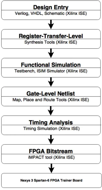
3.2.1 FPGA Design Flow
This Figure 3.3 shows a flow chart for FPGA design [21, 23, 42, 43].
• Before configuring FPGAs, digital designs can be described either by using a hard-ware descriptive language(HDL) such as Verilog and VHDL or as schematic dia-grams created by CAD tools such as Xilinx ISE tools [28] [35]. In HDL modelling, Resister-Translate-Logic (RTL) is the most practical form used to design FPGA chips. RTL description describes the behavior of a digital circuit or hardware de-sign.
• Second, synthesis tools are used to translate the RTL description to create a Gate-Level netlist that describes the connectivity of a digital circuit or design.
• After that, simulation with test-benches is used to verify the functionality of FPGA designs. The test-benches are written in the HDL language used to assign input values for a design. ISIM simulator, from Xilinx ISE Design Suite, is used to simulate and validate the designs in this thesis,.
• Following this, map tools are used to translate the Gate-Level description to logic resources available on an FPGA, while place and route tools are responsible for placing logic resources on the FPGA chip and connecting the design’s logic blocks through programmable routing links.
• Timing analysis comes next to determine the maximum clock frequency that an FPGA design can handle.
• The final step is to produce a bitstream file to configure/program the FPGA. In the thesis, iMPACT tool, from Xilinx ISE tools, is used to conduct this task.
3.3 Chapter Summary
This chapter illustrates the main platform used in this thesis which is the the Dragon12 -Plus board. After that, FPGA fabrics are described, as well as the process of FPGA configuration. In the next chapter, MicroC/OS-II and its functions will be demonstrated.
Chapter 4
MicroC/OS-II
In this chapter, section 4.1 demonstrates MicroC/OS-II. Following this, its functions are explained in Section 4.2. Section 4.3 summarizes the content of the chapter.
4.1 Overview of MicroC/OS-II
MicroC/OS-II is a priority-based, multitasking and hard real-time kernel, commercially released by Micrium Inc., written by Jean J. Lacrosse [24]. In fact, µC/OS-II is an enhanced version ofµC/OS released in 1992. In the second version, Lacrosse added more services to the RTOS and well organized and commented its source code. Micrium’s µC/OS-II is a very robust RTOS, which meets the requirements of safety-critical systems such as railway control systems, braking systems and avionics systems. Additionally, µC/OS-II kernel is open-source, designed to be clean, consistent, well commented, in-depth documented and free for educational, non-commercial uses. Therefore, it is useful for embedded-system studies.
µC/OS-II is a portable, ROMable, scalable, deterministic, priority-based, preemptive and multitasking kernel. It is mostly written in ANSI C with a little Assembly code targeting a specific microprocessor. µC/OS-II has been ported to more than 100 various microprocessors, microcontrollers and digital signal processors (DSPs), so it can run on 8-bit, 16-bit, 32-bit and 64-bit CPU architectures. Also,µC/OS-II requires a small mem-ory footprint, and its user can specify desirable RTOS features and services to be loaded, which reduces the amount of used RAM and ROM. The execution time of any service or function provided by this RTOS is deterministic. Tasks with this RTOS can be inter-rupted or rescheduled according to their priorities, so that the system always dispatches the highest priority task of a set of ready tasks. Context Switch occurs when the RTOS suspends the running task and switches the CPU control to a higher-priority, ready task. µC/OS-II is able to manage up to 64 tasks, eight of which are reserved for the system use, so the RTOS has 64 levels of priority that can be changed dynamically. Furthermore, µC/OS-II use different mechanisms to maintain synchronization and communication be-tween tasks such as event flags, mailboxes and semaphores. µC/OS-II architecture is shown in figure 4.1.
4.2 Functions of MicroC/OS-II
µC/OS-II services are as follows [20, 24]:
• Task management
• Time management
• Inter-task communication and synchronization
• Fixed size Memory management
• Interrupt system management
4.2.1 Task management
µC/OS-II can create, dispatch, schedule, delete, monitor and terminate a task. It has further mechanisms to handle errors, interact and synchronize among tasks. Each task is an infinite loop, and there are five different states, only one of which, a task can be in at any given time, as described in figure 4.2. These states are Dormant, Ready, Running, Waiting and ISR. The RTOS is responsible for tracking and updating each task’s state. If a task is inactive before being created, its state is Dormant. Moreover, a task can either delete itself or get deleted by another task and return from another state to Dormant state until obtaining a new activation signal. After creating a task either by OSTaskCreate() or by OSTaskCreateExt(), the task state changes from Dormant to Ready, and it stays in Ready state as long as another higher priority task is using the CPU. The system
decides based on the task priority which task in a set of ready tasks will run next and be assigned to the CPU. Only one task can be in Running state at any time. OSStart() command is used to start the execution of a task. If a task is in Running state, it can be preempted to execute a higher priority task, and the preempted task returns to Ready state. Also, a running task can be interrupted when an interrupt occurs, and the CPU key registers are stored, and the CPU serves the interrupt by executing ISR. When the CPU finishes executing ISR, it will continue executing the interrupted task as long as there is no higher-priority, ready task. Furthermore, while a task is running, it can be suspended/blocked and change its state to Wait state, waiting for either a resource, a message or a flag. A task can also be delayed for a certain amount of time and stay in Waiting state. Waiting state allows other lower priority tasks to obtain the control of the CPU to execute. After a resource is released or timer is expired, a task returns to the Ready state to be scheduled. Each task must have its own stack to save its state once it has been preempted, suspended or interrupted.
The µC/OS-II uses task control block (TCB) to keep track of status of each task. In fact, µC/OS-II is responsible for updating TCB information in order to be able to schedule and manage multiple tasks. TCB contains a task’s name, state, priority, stack pointer and program counter. TCB is implemented in software as C data structures. There are special tasks including idle task and statistic task. The idle task runs when there are no other tasks running, while the statistic computes the CPU usage.
Figure 4.2: Task States
4.2.2 Time management
µC/OS-II provides a number of services that handle time issues. for instance, OSTimeD-lyHMSM() can delay the execution of the current task by a specific time. OSTimeTick() is a periodic interrupt generated by a hardware timer that defines the clock frequency of the RTOS, which allows tasks to be blocked or suspended for specific times.
4.2.3 Inter-task communication and synchronization
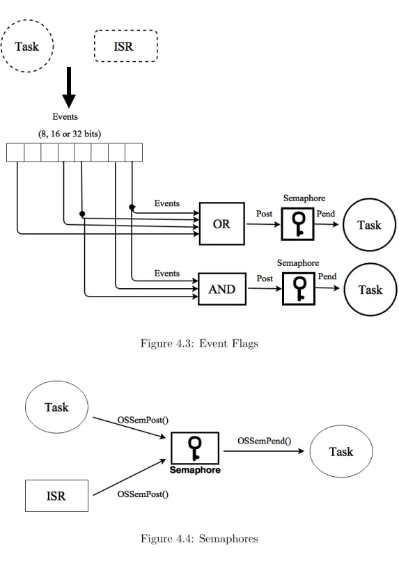
Inter-task communication and synchronization refers to the ways that different task are used to communicate, exchange messages, synchronize their activities and share resources. The RTOS has two mechanisms to synchronize a task with other tasks or ISRs which are event flags and semaphores. In the event flag technique, the synchronization among
tasks depends on the occurrence of events. Event flags are grouped into 8, 16, or 32 bits as described in fig 4.3. This synchronization approach can be performed in two ways: disjunctive (OR) requires that any event occurred, and conjunctive (AND) ensures that all events occurred. Event flags can be set and cleared by either tasks or ISRs; nonetheless, only tasks can wait for events. A semaphore is a classical wait signal operation in which a task waits on a semaphore until getting a signal to resume its execution. OSSemPend and OSSemPost are two important services that µC/OS-II provides to handle a semaphore. Whereas OSSemPost generates a signal that releases a semaphore, OSSemPend makes a requesting task wait on a semaphore until being released. Fig 4.4 clearly demonstrates the mechanism of semaphores.
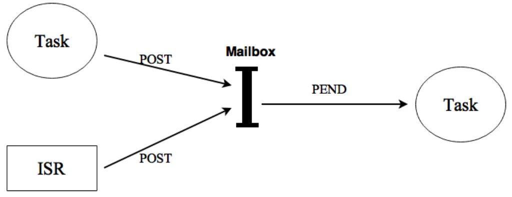
Inter-task communication is when the processes need to communicate with each other in order to consistently cooperate. TheµC/OS-II provides several mechanisms to main-tain inter-task communications including message mailboxes and messages queues. Mes-sage mailboxes and mesMes-sages queues are services that µC/OS-II provides in order to allow a task or ISR send one or more messages to a task. Fig 4.5 describes a mailbox and message queue.
Figure 4.3: Event Flags
Figure 4.5: Message Mailboxes
4.2.4 Fixed size Memory management
In preemptive systems, each task must have its own stack to store the key registers when being preempted. Stack allocation and de-allocation can be achieved by using ”malloc” and ”free” functions in C-language. These functions may lead to memory-fragmentation issues. µC/OS-II provides a solution for memory fragmentation by allowing application tasks to use fixed-sized memory blocks made of contiguous memory area.
4.2.5 Interrupts and ISR
The RTOS can also keep track of interrupt nesting by using OSIntEnter and OSIntExit commands to serve or exit an interrupt service routine (ISR). Interrupts can be nested up to 255 levels. Critical Sections are codes areas that run by µC/OS-II without being interrupted or preempted. For this, µC/OS-II disables all interrupts when executing a critical code, and then the RTOS kernel re-enables interrupts after leaving critical sections. There are two macros including: OS Enter Critical and OS Exit Critical, used to disable and enable interrupts. To illustrate, there are three methods to implement these macros depending on the microprocessor and compiler. The first Method is the simplest one, and it first disables interrupts when entering a critical section and then enables all disabled interrupts after finishing the execution of a critical function. In the second method, the interrupt disable status is saved when entering a critical section and then restored when leaving a critical section. Compared to the first method, the second one does not change the interrupt status. The third method stores the processor interrupt
status into a local variable when executing a critical function and restores the value back to the processor interrupt status upon the completion of the critical section.
4.3 Chapter Summary
This chapter explores the MicroC/OS-II and its features and functions. In the next chapter, the steps of implementation followed in this thesis will be illustrated.
Chapter 5
Implementaion
In this thesis, Serial Peripheral Interface (SPI) protocol is established in hardware and software on the Nexys3 and Dragon12-Plus boards respectively to allow these platforms communicate and exchange data and control signals. The main motivation behind this is to demonstrate the concept of integrating software processes performed by a real-time operating system with hardware processes implemented on FPGA fabrics.
In this chapter, section 5.1 provides a brief overview of Serial Peripheral Interface (SPI) protocol. Section 5.2 illustrates the configuration of SPI master on the HCS12 microcon-troller board. The FPGA implementation of SPI slave is presented in section 5.3 as well as parallel port.
5.1 Overview of Serial Peripheral Interface (SPI)
SPI is one of the most common serial, low-end communication protocols in master/slave mode [15,29,31] . It provides full duplex, synchronous and slow/medium data-transmission
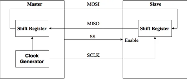
between a microcontroller and other peripheral devices such as DACs, ADCs and EEP-ROMs. As demonstrated in diagram 5.1, a master component is responsible for initiating data transmission and configuring and selecting a slave component. For synchronization purposes, there is a common clock generated by the master to control the rate of data transmission, denoted by SCLK. The master configures the clock polarity (CPOL) and phase (CPHA). MOSI and MISO are serial and single-bit data lines to exchange data signals between the master and slave. Slave Select is an active low signal used by the master to activate/select the slave device. Two 8-bit shift registers are used to shift data out with the most significant bit first to exchange data between the master and slave. The table 5.1 describes the recent specifications of SPI protocol [33, 34]. In the thesis, the HCS12 acts as the SPI master device, while the FPGA is the SPI slave component.
Table 5.1: SPI Specifications
Feature SPI
M anuf acturer Motorola (1979) P lug−and−P lay No
Interf ace type Serial (3+N wires)
Distance Short
Application Transfer of data-streams P rotocol Complexity Simple
T ransf er rate Up to 4MHz P ower Consumption low
T ransf er type Full Duplex T ime Constraint Synchronous M ulti M aster No
M ulti Slave Yes
5.2 Configuration of SPI Master
To use the HCS12 microcontroller as SPI master, several registers have to be configured according to the programmer’s requirements.
First, SPI interface has to be initialized as follows:
(1) Configure the upper part of the DDRS register with the appropriate value to use them as SPI four wires (MOSI, MISO, SS, SCLK).
(2) Configure the five SPI registers with the desirable parameters and values: • One baud rate generator register (SPIBR) to define data transfer rate. • Two control registers (SPICR1, SPICR2) to set up SPI control parameters. • One data register (SPIDR) to read and write data.
• One status register (SPISR) to determine the status of the transfer.
To send data through SPI from the HCS12 microcontroller to the FPGA:
(1) Store data into SPIDR (SPI Data Register).
(2) Check SPISR (SPI Status Register) to determine whether or not sending data is completed.
To receive data through SPI by the HCS12 microcontroller from the FPGA:
(3) Store the content of SPIDR into a variable.
The Dragon12 -Plus board is the main platform for the thesis implementation. The code for the SPI master is written in C language and embedded in Micrium’s C/OS-II and ported to a HCS12 microprocessor. A new software task, called SPI task, has to be created and added to the application file of theµC/OS-II. The HCS12 microcontoller is the master device which is responsible for assigning the frequency rate and sending data that needs to be manipulated on FPGA fabrics, so the SPI task is programmed to configure the microcontroller’s SPI pins to manage data and control signals. Other tasks including data task and receiving task are created. The data task is responsible for providing data for the SPI task, and they communicate and exchange data through mailboxes, while the receiving task is an event-triggered task that waits for a flag is set by a hardware interrupt signal coming from the FPGA platform. Furthermore, C files and header files of the SPI master are added to the board support package (BSP) file of theµC/OS-II. Port E is also configured, which has two input pins (PE0, PE1), while the remaining pins are configurable to be either input or output. PE0 and PE1 might be used for external interrupts lines: IRQ and XIRQ. In this work, pin PE0 is used as input for IRQ external interrupts line. Interrupt service routine is written to handle an IRQ pin interrupt, and interrupt vector is modified. To illustrate, The HCS12 MCU responds to program instructions in a sequential manner except for interrupts and resets. When a specific interrupt is triggered, the CPU stops the execution of the main program and switches to perform Interrupt Service Routine (ISR), and CPU registers are temporarily
stored. After that, the program goes to the interrupt vector table that contains the actual addresses of ISRs. While the addresses in the vector table are fixed, the ISR addresses are changeable determined by the programmer. Upon the completion of ISR, CPU registers are restored to return to the main program execution. The benefits of using interrupts are to improve the CPU usage and to efficiently handle I/O devices’ operations.
5.3 FPGA implementation of SPI Slave
The FPGA board represents the slave device which is responsible for processing data that is received from the microcontroller. The coding of SPI Slave is implemented using Verilog HDL on Xilinx ISE Project Navigator Ver. 14.7, and the SPI slave is tested and verified on the Digilent Nexys3 FPGA board. Fig 5.2 describes the RTL schematic diagram.
A parallel interface module has to be designed on the FPGA board in order to first send an interrupt request signal and then send results from the FPGA to the HCS12 microcontoller platform. Fig 5.3 describes the final design diagram.
Figure 5.2: RTL Schematic of SPI Slave
Table 5.2 provides the logic utilization summary of the SPI slave design implemented on the Xilinx Spartan-6 FPGA Board, using Xilinx Integrated Software Environment (ISE) Project Navigator Ver. 14.7.
Table 5.2: Synthesis Summary of SPI Slave
Logic Utilization Used Available Utilization Number of Slice Registers 65 18,224 1%
Number of Slice LUTs 77 9,112 1%
Number of Bounded IOBs 69 232 29%
5.4 Chapter Summary
This chapter describes the configuration and implementation of the SPI master and SPI slave on the EVB Plus development board and the Nexys 3 board respectively. In the following chapter, the design example will be demonstrated, which is a satellite attitude controller.
Chapter 6
Design Example: Satellite
Attitude Controller
This chapter describes the hardware implementation of a satellite attitude control system using VSC on the Nexys3 FPGA for floating point and fixed-point implementations. Furthermore, it presents the calculations of power consumption and logic resources for the design of the satellite controller. The coding of satellite attitude controller is developed using Verilog HDL on Xilinx ISE Project Navigator Ver. 14.7, and this design is tested and verified on the Digilent Nexys3 Spartan-6 FPGA board.
Section 6.1 reviews the issue of satellite attitude control. Section 6.2 describes a Hardware in the loop (HiL) technique. Following this, a variable structure control method is illustrated in section 6.3. After that, section 6.4 demonstrates the Implementation of satellite attitude control system using Variable Structure Control, and it also provides the results of testing the attitude control system.
6.1 Overview of Satellite Attitude Control
Controlling the position and attitude of a satellite is one of the most vital task in satellite functions. The objective of a satellite attitude control system is to produce a smooth/even movement for a satellite through its orbit in order to stabilize it. Such systems need to be subjected to reliability, low power consumption, weight and time constraints due to their extremely remote operating environment. In case of a failure in the satellite control system, catastrophic scenarios such as losing spacecrafts may occur. Investigation concluded that the main reason for failure is an error in the attitude control system [19,30]. In this thesis, a 2-input satellite attitude controller is implemented on the Nexys3 Spartan-6 FPGA board to study the effect of jitter and noise on the controller performance. The HiL model is further used to study the controller performance using both floating point representation and fixed point representation.
6.2 Hardware in The Loop (HiL)
Hardware in the loop (HiL) is a simulation technique in which the control system model is replaced by actual hardware. In contrast to traditional techniques in designing control systems, HiL provides an effective platform to bridge the simulation, implementation, and testing [4]. In this work, an FPGA platform is proposed for hardware in the loop emulation of satellites in a satellite attitude control system, and an HiL emulator of the satellite and a satellite attitude controller are constructed using actual hardware to be
point vs. floating point representation, and jitter on the controller performance.
6.3 Variable Structure Control (VSC)
Variable structure control (VSC) with sliding mode is used to model satellite attitude controller. VSC is a discontinuous nonlinear control technique that is insensitive to the variations in system parameters which are restricted to certain matching conditions. In fact, VSC is capable of controlling uncertain systems whose parameters may vary within known boundaries. The VSC method alters the dynamics of a system by the application of a discontinuous control signal that forces the system to ”slide” along a cross-section of the system’s normal behavior. Thus, this mode of the system operation is known as Sliding Mode Control (SMC). Despite parameter variation and system uncertainties, the system state variables in SMC mode are forced to stay on a predefined switching surface that determines the desired dynamics of the system. SMC has been applied suc-cessfully to control many various physical systems with uncertainties [44]. The SMC control technique has many attractive features such as fairly straightforward firmware implementation, robustness, finite-time convergence, and reduced-order compensated dy-namics. SMC is insensitive to small disturbances during the sliding mode by forcing the system dynamics to stay on an desired sliding surface using discontinuous control laws characterized by high gain and high switching frequencies. However, These control laws´characteristics are the main drawbacks of using SMC. To illustrate, high gain control can violate the control saturation constraints, especially during the transient stage. High
switching frequency results in a chattering problem which may cause the system insta-bility [12]. There are many approaches to solve the chattering issue such as boundary layer technique and adding an auxiliary control input to the system as fuzzy control. More recent contributions have extended the sliding mode control and introduced the concept of higher order sliding mode control in order to seek a smooth control that will naturally and accurately encompass the benefits of the traditional approach to sliding mode control.
In the sliding mode, defining the desired sliding mode dynamics is attained and main-tained by means of solving the reachability problem.
6.4 Implementation of a Satellite Attitude Control system
To control the attitude of spacecraft, a mathematical model of the spacecraft should be derived first. The mathematical model of the spacecraft motion describes the translation and attitude motion of the spacecraft under the influence of external actuators’ forces and torques. These equations are highly coupled nonlinear differential equations that makes it hard to implement using most common control techniques. Therefore, the exact model will be simplified by a linearization technique around the equilibrium state.
The attitude of the space station relative to the desired earth-pointing attitude can be defined using the three angles; the pitch θ1, the yaw θ2, and the roll θ3. When the
A simplified nonlinear model of the spacecraft can be found in [26] ˙ Θ =RΩ +n (6.1) IΩ =˙ −Ω×IΩ + 3n2I c−U (6.2) ˙ h= Ω×h+u (6.3) Where R(Θ) = 1 cosθ3
cosθ3 −cosθ1sinθ3 sinθ1sinθ3
0 cosθ1 −sinθ1
0 sinθ1cosθ3 cosθ1cosθ3
c= −sinθ2cosθ3
sinθ−1 cosθ2+ cosθ1sinθ2sinθ3
cosθ1cosθ2−cosθ1sinθ2sinθ3
n= 0 n 0 , Ω = ω1 ω2 ω3 , Θ = θ1 θ2 θ3 , U = u1 u2 u3
U is the control moment gyro input vector,Ω is the angular velocity,I is the moment of inertia matrix,nis the orbital angular velocity, Θ is Euler angles,h is the total control
moment gyro momentum, and the moment of inertia matrix is diag[1989 1876 407] as shown in [13].
After linearizing the model around Θ = [0 0 0], Ω = [0 −n0], and assuming that the spacecraft has zero product of inertia, and also the aerodynamic disturbance is negligible. The roll/yaw axes in the system can be represented as
˙ X= 0 n 1 0 −n 0 0 1 −3n2∆1 0 0 −n∆1 0 0 −n∆2 0 X+ 0 0 0 0 −1 I1 0 0 −I1 3 U (6.4) Where ˙ x= ˙ θ1 ˙ θ2 ˙ ω1 ˙ ω2 , u= U1 U2 , ∆1 = I2−I3 I1 , ∆2 = I1−I2 I3
A = 0 0.0042 1 0 −0.0042 0 0 1 −3.91×10⁻⁵ 0 0 −0.0031 0 0 −0.0012 0 B = 0 0 0 0 −0.0005 0 0 −0.0025 Where U is the input.
X is the state vector X= [yaw angle , roll angle , yaw rate , roll rate]0.
The eigenvalues of the system are 0 + 0.0076i,0−0.0076i,−0.0021,0.0021. Note that the system is inherently unstable. However, it is not difficult to prove that the system is controllable.
In order to use the sliding mode control, it is easier to transfer the state space equa-tions of the system to a canonical controllable form. Note that since the rank of the controllability matrix [b1 b2 Ab1 Ab2] is 4 (the system order), the system is controllable.
T = −1980 0 0 0 0 −407 0 0 0 −8.4 −1989 0 1.7 0 0 −407 (6.5)
The system now is represented in the new coordinates ˙
Z =AzZ+BzU whereZ =T X, Az =T AT−1, Bz =T B
The sliding mode controller can be designed using the state space in the new coordi-nates system. The 2 switching surfaces are simply algebraic equations expressed in terms of the states and the desired eigenvalues λ1 and λ2. Here, λ1 = −1 and λ2 = −2. The
switching surface equation is
σ(Z) =CZ= 0 C = λ1 0 1 0 0 λ2 0 1
The C matrix will be used to design the controller in section 6.4.2.
6.4.1 Model Implementation
The input to the model is the vector U, which is the output of the controller. After the system is discretized, the following difference equation is conducted.
x(k+ 1) =Ad×x(k) +Bd×u(k) (6.7)
whereAd andBdare the discrete version of the matricesAand B,u(k) andx(k) are
the values of the variablesU andXat discrete points of timekT,0≤k≤ ∞,T is the time step. Since the hardware emulator should be as close as possible to the continuous system, if the non-linear continuous system is emulated, the time step in the HiL calculation must be much smaller than the controller cycle time (controller time step). however, since the linear model is used, the time-step of the emulation is the same as the time step used in the controller design. With a discretization step of 1msec, the following matrices are obtained. Ad = 1 0 0.001 0 0 1 0 0.001 0 0 1 0 0 0 0 1 (6.8) Bd = 5×10⁻⁷ 0 0 5×10⁻⁷ 0.001 0 0 0.001 (6.9)
The HiL implements equation 6.7. It takes the values of the current state (X) and the input (U) from the controller to produce the next state. The new state is sent to the controller to produce the next input and so on. Beside producing the next state, the model should be able to do two things.
1. It should be able to add a random noise to the values of the states sent to the controller to emulate error in sensing and transmission.
2. It should be able to delay sending the value of the state to the controller in order to emulate jitter in the controller.
The linearized model is implemented, proposed in Eq 6.7. The hardware is designed to emulate the above model. Another point to consider is what hardware should be used for the model. A microcontroller is a reasonable choice, however it suffers from the same timing unpredictability, Cache miss, interrupts, and dynamic scheduling. Such implementation can not guarantee a very predictable calculations.
FPGA looks like a much better alternative. Its flexibility, ease of configuration, hard-ware dedication, and ease of rapid prototyping are very important characteristics. This model is implemented using Xilinx Spartan-6 XC6SLX16 in Digilent Nexys-3 board for the implementation [18].
As shown in Fig 6.1 above, the HiL model is built on the FPGA chip. The controller is also implemented the controller on the same chip. This is not a limitation, since the output of the model is available on the chip output so it could be used with an external
Satellite Model U
Controller X
FPGA CHIP Noise
ref(t) delay
Figure 6.1: A schematic view of the emulator and controller
Fig 6.1 shows the system with the controller and the model connected. Both the model and the controller are implemented on the same FPGA. The model calculates theX vector and sends it to the controller; the controller calculates the input U vector and sends it to the model. The reference signal is supplied to the controller as ref(t) (the desired value of X). The solid black box on the X link going from the model to the controller adds random noise to the value transmitted in order to simulate error in sensing; that operation is controlled by a strobe signal that allows us to either add or not to add the noise. The random noise is chosen to emulate a specific SNR. The box on theU input to the satellite model is a shift register that is used to delay the input for a specific number of cycles before it is delivered to the model in order to simulate jitter in the calculation by the controller.
The hardware required for model implementation consists of a matrix vector mul-tiplication, vector vector mulmul-tiplication, an adder and the glue logic. The design is implemented on a Nexys-3 board [18] with a Spartan-6 XC6SLX16 chip [46].
U B X A X X + Noise delay X U
Figure 6.2: Block diagram of the satellite model
satellite model in Eq. 6.7. Where A is the 4-by-4 matrix Ad, X is the state variables
vector, B is the Bd vector, and U is the control input from the controller in order to set
the required values forX.
The model updates the value of the X vector. Random noise is added to the output before it is transmitted to the controller (that represents noise added to the measured value of X either sensing noise, or noise added to the signal during transmission).
In real life, where the controller is doing more than ”attitude control” the controller might be delayed responding to the incoming signal. This delay may come from many sources. Some higher priority tasks may delay the response, time variations in executing the programs because of cache state, or because Interrupts might take more than expected. This is simulated by by holding theU input in a buffer for a random period of time. The delay is implemented by a handshaking mechanism for sending the information to the controller; the handshake is delayed by using a buffer that delays the transmission for a
random period of time.
Since the model is implemented on FPGA (synchronous logic) in order to add delay, the system has to run at a much higher frequency than the controller and model are working at. In that case, delay means skipping a specific number of cycles before the sampled value are delivered to the controller.
Note also that Fig 6.2 shows only the datapath of the architecture. An FSM is constructed to control the data flow between the modules, adding random noise and controlling the delay.
The model was implemented on Xilinx XC6SLX16 in Digilent Nexys-3 board. 32-bit fixed point representation is used (this is the most widely used standard especially for D/A conversion and sensing).
6.4.2 Controller Implementation
In a previous work [1], a single input controller is implemented for satellite attitude control. The advantage of using one input is simplicity of the system design. However, using a single control input resulted in a long settling time tens of minutes in some cases. Here, a 2-input controller is implemented. The settling time is in the range of few seconds. The controller is implemented on the same chip as the system model. There is no reason to implement the controller on the same chip as the model. The controller could be implemented as software on a microcontroller or any separate hardware. As a matter of fact, the main reason to implement the HiL is to use it to test any controller. However,
for simplicity, an on-chip controller is used.
In this thesis, VSC is applied for satellite attitude control. VSC systems comprise a collection of different, usually quite simple, feedback control laws and a decision rule that is designed to force the system states to reach, and subsequently remain on, a predefined surface within the state-space, depending on the status of the system. The dynamic behavior of the system in order to reach the switching surface is called the reaching mode, while the dynamic behavior of the system when confined to the surface is named
theideal sliding motion mode.
The repositioning of the geostationary communication satellite could be achieved using many techniques. To produce the required torque; it can be used thruster, momentum wheel, magnetic torquer and so on. Magnetic control is the most economical way to stabilize a satellite, despite the fact that its torque is weaker than the torque produced by a thruster or control moment gyro; the magnetic control does not consume fuel and thus does not result in changing the satellite mass over time. In addition it is simpler to implement and lightweight compared to other torque producing methods. The controller design [13] is as follows:
the switching service is defined as
S=C×Z where Z =T ×X (6.10)
The switching surface vector is
C = λ1 0 1 0 (6.11)
and the conrntrol input is calculated as U(i) = −Ks sign(si) si > −Kn×Z si < where k= 30 [13]. 6.4.3 Fixed Point
The IEEE 754 floating point representation is a standard representation used almost exclusively in all desktops and laptops computers [2]. The multiplication and addition of standard floating point numbers are rather complex operation. Especially for addition, where the two numbers have to be converted to a common exponent, perform the addition and then normalizing the number through shifting. For small embedded calculations, and when the accuracy and dynamic range of floating point numbers are not needed, simpler fixed point representation(Qm.n) format can be used a.
The Qm.n format forN-bit binary number consists of 2 parts separated by an implied binary point. The left most m bits is the 2’s complement representation of the integer part of the number. The fraction part is represented by thenrightmost bits. An implied binary point separating the 2 parts (note thatm+n=N), and thenfraction bits have a negative exponent. Arithmetic operations on fixed point number are integer operations and thus faster than floating point operations.
Many values are experimented for m and n in order to find a good result. it has been found out that Q9.9 gives almost identical results as floating point representation, while any thing less than Q7.7 results in an unstable system. Three values are used for fixed point representation, Q9.9, Q8.8, and Q7.7. Fig 6.3 showsθ1 response for different values
of Qm.n and compares it with floating point representation. From the figure, it can be seen that there is almost no difference between floating point representation and Q9.9 (the 2 graphs completely overlaps). It is also noticeable that for Q8.8, there is a small difference between Q8.8 and floating point, the difference is aggravated in the case of Q7.7. Fig. 6.4 shows the input for the above different cases. The results for θ2 is almost
6.4.4 Discussion and Observations
Table 6.1 shows the power consumption and the chip resources required for the controller implementation using floating point and fixed point representation [2]. For the different resources, the number indicate the number of units of that resource used in the design, while the number between parenthesis gives the percentage of that resource used in the design). For example, Q9.9 implementation requires 315 LUTs which accounts for 3% of LUTs in the chip. Power consumption for fixed point is almost 50% of the floating point representation. However, the biggest saving is in the LUT’s and slices use. The number of used slices goes down from 32% to 4% and 3% respectively, although the performance of Q9.9 is almost identical to floating point representation.
Table 6.1: The implementation cost of the fixed-point representation controller
float. pt. Q9.9 Q8.8 Q7.7
power (mW) 101.3 60.5 55.9 48.8
LUT 2278(25%) 315 (3%) 257 (2%) 224 (2%)
6.5 Chapter Summary
In this chapter, the design and implementation of a satellite attitude control system based on Field programmable Gate Array (FPGA) technology is demonstrated to illustrate the thesis work.
Chapter 7
Conclusion and Future Research
Directions
This chapter summarizes the main results of the thesis and outlines research directions for future work.
In this thesis, µC/OS-II has been modified in order to manage hardware processes implemented on the Nexys 3 Spartan-6 FPGA Board. The EVBplus HCS12 development board was the main prototype platform hosting µC/OS-II kernel. The first contribution was to implement Serial Peripheral Interface (SPI) protocol in hardware and software on the Nexys3 and Dragon12-Plus boards for communication purposes. After that, the C and header files of the SPI and parallel interface are added the board support package (BSP) file of the µC/OS-II. Following this, ISR is added to the board support package (BSP) file of theµC/OS-II to handle hardware processes performed on the FPGA board. The final contribution was to design hardware implementation of a satellite attitude control
system using variable structure control (VSC) and the hardware-in-the-loop emulator on the Nexys3 FPGA board for fixed-point and floating point representations. Power consumption and logic resources are further calculated for the design of the satellite controller for fixed-point and floating point representations .
For future developments, in-dept modifications onµC OS/II kernel and partial config-uration of a FPGA platform would be achieved to add more support for hardware-process management. It is further recommended that the communication protocols be improved in future work.
Bibliography
[1] M. Aboelaze, O. El Debb, A. El-Bayoumi Mansour, and M. Ghazy Shehata. FPGA implementation of a satellite attitude control using variable structure control. Proc. of the MIC Computing, 2014.
[2] M. Aboelaze, M. Shehata, and S. Atiwa. A hardware in the loop emulator for a satellite control system. the International Journal of Embedded Systems. accepted Sept. 2016.
[3] L. Anders, K. H. Andersen, U. P. Schultz, and A. S. Sørensen. HartOSA hardware implemented RTOS for hard real-time applications. IFAC Proceedings Volumes, 45(7):207–213, 2012.
[4] M. Bacic. On hardware-in-the-loop simulation. In Proceedings of the 44th IEEE Conference on Decision and Control, pages 3194–3198, Dec 2005.
[5] S.F. Barrett and D.J. Pack. Embedded Systems Design and Applications with the 68HC12 and HCS12. Pearson/Prentice Hall, 2005.
![Figure 3.2: Nexys 3 Spartan-6 FPGA Trainer Board [18]](https://thumb-us.123doks.com/thumbv2/123dok_us/1079405.2643666/29.918.293.696.476.811/figure-nexys-spartan-fpga-trainer-board.webp)