66
Calculation of Characteristics
of the Single Electron Transistor
Nguyen The Lam*
Faculty of Physics, Hanoi Pedagogical University No. 2, Nguyen Van Linh, Xuan Hoa, Phuc Yen, Vinh Phuc, Vietnam
Received 24 August 2015
Revised 15 October 2015; Accepted 18 November 2015
Abstract: This paper will show that the characteristics of Single Electron Transistor (SET) may be calculated. In the model of SET, the electrons are transferred one-by-one through the energy potential barriers by tunneling and a quantum dot is formed between two barriers. By determining the wave functions in the regions, we have calculated the transfer coefficient of SET. The other characteristics of SET as, currents through the Source and Drain regions, electron density in the quantum dots and I-V characters are also calculated and investigated.
Keywords: Single Electron Transistor, SET, quantum dot in the SET, transfer coefficient of SET.
1. Introduction∗∗∗∗
The Single Electron Transistor [SET] have been made with critical dimensions of just a few nanometer using metal, semiconductor, carbon nanotubes or individual molecules. The operation of most SET depends on the formation of a very thin conducting layer of electrons, which is formed at a pn-junction (for example, AlGaAs/GaAs). In the layers of this nature, electrons flow laterally along the heterojunctions. A SET consist of a small conducting island (Quantum Dot) and is coupled to the source (S) and drain (D) by tunnel junctions and capactively coupled to one or more gates (G) [1]. Unlike Field Effect Transistor (FET), the single electron device based on an intrinsically quantum phenomenon, the tunnel effect. In the FET, many electrons transmit from the Source to Drain and make current, in the SET, the electrons is transferred one-by-one through the channel. The electrical behavior of the tunnel junction depends on how effectively the electron wave transmit through the barriers, which decrease exponentially with the thickness and on the number of electron waves modes that impinge on the barriers. It is given by the area of tunnel junction and divided by the square of wave length [2].
_______ ∗
Tel.: 84- 989387131
Fig.1. The Schematic of a Single Electron Transistor [SET] (a) and the model for double barriers of the SET (b)
The SET consists of two electrodes known as thedrainand thesource, connected through tunnel junctions to one common electrode with a low self-capacitance, known as the island. The electrical potential of the island can be tuned by a third electrode, known as thegate, capacitively coupled to the island (figure 1-a) [3].
In the our model, the tunneling of the electrons through double-barriers is described in figure. 1(b). Where, The energy barriers are formed by two semiconductors with the different energy band gaps (for example AlGaAs/GaAs). The heights of barriers are V1 and V2, which are the difference between
two band gaps of the semiconductors. The widths of barriers are W1 and W2 respectively, which are the
thickness of the semiconductor with the wider band gap (for example AlGaAs). The Gate regions is described as a quantum dot with the width is L and the shift of the bottom is Vm. The energy of
electron (holes) is supported by apply a voltage between S and D electrodes. The energy E of electron (holes) in our model is always satisfied the condition that, E is much smaller than the V1 and V2. The
shift of energy in the quantum dot is controlled by an applied voltage on the G electrode.
2. Basic eqution and transfer matrix
The motion of the electron from S region to D region is described by the Schrodinger equation in the one dimensional system.
2
''( ) ( ) ( ) ( )
2mψ x V xψ x Eψ x
− + = (1)
Where, V(x) is the energy potential, m is the mass of the electron and is the Flank constant. In
the region I (Source), V(x) = 0. In the region II (barrier 1), V(x) = V1. In the region III (Gate), V(x) = Vm. In the region IV (barrier 2), V(x) = V2. In the region V (Drain), V(x) = 0. The wave function in
these regions are written in form
1( ) . . with
ikx ikx
L R
x A e A e x a
ψ −
= + ≤
1 1
2( ) . . with a
ik x ik x
L R
x B e B e x b
ψ −
= + ≤ ≤
(a)
V2
V1
W1 L W2
Vm
Source Zone
Gate Zone
(QD) Drain
Zone
E
n
e
rg
y
(
E
)
3( ) . . with
m m
ik x ik x
L R
x C e C e b x c
ψ = + − ≤ ≤ (2)
2 2
4( ) . . with c
ik x ik x
L R
x D e D e x d
ψ = + − ≤ ≤
5( ) . . with
ikx ikx
L R
x E e E e x d
ψ = + − ≥
where the wave vectors are defined:
2 2 ; mE k=
(
)
2 1 1 2 ;m V E
k = −
(
)
2 2 2 2 ;m V E
k = −
(
)
2
2 m
m
m V E
k = −
(3)
The coefficients AL, AR, BL, BR, CL, CR, DL, DR, EL, ER from the equation system (2) may be
calculated by boundary conditions (the wave functions and their first derivatives must be continuous across each interface).
From the conditions for the wave function and their first derivative are continuous at the interface between I and II regions, we have an equation system for transfer matrix and transfer coefficient in this interface.
1 1
1 1
1 1
ik a ik a
ika ika
L R L R
ik a ik a
ika ika
L R L R
A e A e B e B e
ikaA e ikaA e ik aB e ik aB e
− − − − + = + − = −
(4)
Rewrite system (4) in the matrix form, we have
1 1
1 1
1 1
ik a ik a
ika ika
L L
ik a ik a
ika ika
R R
A e e B
e e
A ik ae ik ae B
ikae ikae − − − − = − −
(5)
or
1
12 2
L L L
R R R
B m A A
T
B m A A
= =
(6)
where, we introduced
1 ika ika ika ika e e m ikae ikae − − = −
and
1 1
1 1
2
1 1
ik a ik a
ik a ik a
e e
m
ik ae ik ae
−
−
=
−
(7)
and T12 is the transfer matrix between I and II regions. For more further, we rewrite the transfer matrix
in the form.
12 12
12 12 12
RR RL LR LL T T T T T =
(8)
The transfer matrices contain all physical information about scattering. The amplitude of the transmitted wave is
12 12
in
out LL
k k T
τ = (9)
12 12
1
LL
T
τ = and 12 2
12
1
LL
t T
= (10)
In similar way, we can determent the transfer matrix for other interfaces
2
23 3
L L L
R R R
C m B B
T
C m B B
= =
, 23 23
1
LL
T
τ = and 23 2
23
1
LL
t T
= (11)
3
34 4
L L L
R R R
D m C C
T
D m C C
= =
, 34 34
1
LL
T
τ = and 34 2
34
1
LL
t T
= (12)
4
45 5
L L L
R R R
E m D D
T
E m D D
= =
, 45 45
1
LL
T
τ = and 45 2
45
1
LL
t T
= (13)
where
3
m m
m m
ik a ik a
ik a ik a
m m
e e
m
ik ae ik ae
− − = − , 2 2 2 2 4 2 2
ik a ik a
ik a ik a
e e
m
ik ae ik ae
−
−
=
−
and m5 = m1 (14)
The propagation of the electron (hole) from Source region to Drain region is then described by the product of the transfer matrices:
45 34 23 12
L L
R R
E D
T T T T
E D
=
and 45 34 23 12
L R L R E E T T T T T
D D ⇒ = = (15)
and the transmission coefficient τ and transmission probability t are as follows
1
LL
T
τ = and 1 2
LL
t T
= (16)
3. The results and discussions
The model for calculation of characteristics of the SET is built and shown in figure 2 [6]. Where, the heights of the energy barriers are V1 = V2 = 0.3 eV for the Al0.3Ga0.7As/GaAs [7,8] and V1 = V2 =
0.1 eV for the Al0.1Ga0.9As/GaAs [8,9]. The widths of the energy barriers are the thickness of the
AlGaAs layer and that is 70 nm. The width of the quantum dot is the thickness of GaAs layer in the middle and L = 300 nm.
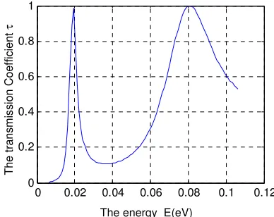
From the formula of the transmission coefficient τ (10), (11), (12), (13) and (16), we can find out the dependence of transmission coefficient τ on the energy E. The peaks of the transmission coefficient are located in the energy levels of quantum dots. The peaks in the higher energy levels are higher and wider than themselves in the lower energy levels. The results are shown in figure 3 and 4. When the height of the energy barrier decrease, the resonant peaks are moved forward to the lower energy (figure 4). The first peak is higher and the second peak is wider. An other theoretical study of electronic transmission in resonant tunneling Diodes based on GaAs/AlGaAs double barriers under bias voltage [10] with different model has obtained a similar transmission coefficient as function of incident energy. Our results of the transmission coefficient are good agreement with [10].
0 0.1 0.2 0.3 0.4
0 0.2 0.4 0.6 0.8 1
0 0.02 0.04 0.06 0.08 0.1 0.12
0 0.2 0.4 0.6 0.8 1
Fig. 3. The transmission coefficient of the SET Al0.3Ga0.7As/GaAs. Where W1 = 70 nm, W2 = 70
nm, V1 = 0.3 eV, V2 = 0.3 eV, Vm= 0 eV and L =
300 nm.
Fig. 4. The transmission coefficient of the SET Al0.1Ga0.9As/GaAs. Where W1 = 70 nm, W2 = 70
nm, V1 = 0.1 eV, V2 = 0.1 eV, Vm= 0 eV and L =
300 nm.
The current through the S and D regions are defined as following:
min
( )
S
S
J E dE
µ
ε
τ
=
∫
andmin
( )
D
D
J E dE
µ
ε
τ
=
∫
(17)Where εmin is the lowest energy of electron, µS and µD are Fermi level in the S and D regions
respectively. Calculating the integrates in (17) numerically, the current JS and JD are shown in figure 5
and 6.
The electronic density on the energy is defined as follow
2
0
( ) ( )
L
N E =
∫
ψ x (18)So the electronic density on the energy in the quantum dot are shown in figure 7 and 8. The energy E(eV)
T
h
e
t
ra
n
s
m
is
s
io
n
C
o
e
ff
ic
ie
n
t
τ
The energy E(eV)
T
h
e
t
ra
n
s
m
is
s
io
n
C
o
e
ff
ic
ie
n
t
τ
0 0.1 0.2 0.3 0.4 0 0.5 1 1.5 2 2.5x 10
-14
0 0.02 0.04 0.06 0.08 0.1
0 1 2x 10
-14
Fig.5. Current Js (square), JD (triangle) and Jtotal
(open circle) of the SET Al0.3Ga0.7As/GaAs. Where
W1 = 70 nm, W2 = 70nm, V1 = 0.3 eV, V2 = 0.3 eV,
Vm= 0 eV and L = 300 nm. The µS = 0.5V1 and µD
= 0.4V2.
Fig.6. Current Js (square), JD (triangle) and Jtotal
(open circle) of the SET Al0.1Ga0.9As/GaAs.
Where W1 = 70 nm, W2 = 70nm, V1 = 0.1 eV, V2 =
0.1 eV, Vm= 0 eV and L = 300 nm. The µS = 0.5V1
and µD = 0.4V2.
0 0.1 0.2 0.3 0.4
0 1 2 3 4 5 6x 10
-6
0 0.02 0.04 0.06 0.08 0.1 0.12
0 0.5 1 1.5 2 2.5x 10
-6
Fig.7. The electronic density on the energyof the SET Al0.3Ga0.7As/GaAs. Where W1 = 70 nm, W2 =
70nm, V1 = 0.3 eV, V2 = 0.3 eV, Vm= 0 eV and L =
300 nm.
Fig.8. The electronic density on the energy of the SET Al0.1Ga0.9As/GaAs. Where W1 = 70 nm, W2 =
70nm, V1 = 0.1 eV, V2 = 0.1 eV, Vm= 0 eV and L
= 300 nm.
From these figures, we see that, the peak in the first energy level is much higher and sharper than the peaks in the excitation energy levels.
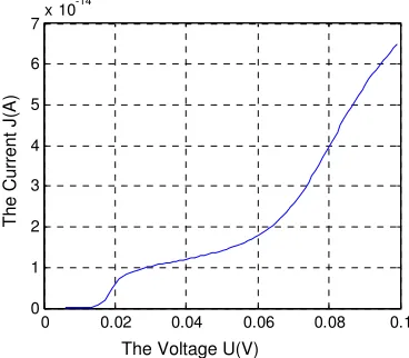
The I-V characteristics of SET is also calculated in the formula
min / 2 / 2 ( ) S U S U
J E dE
µ
ε
τ
+
+
=
∫
andmin / 2 / 2 ( ) D U D U
J E dE
µ
ε
τ
−
−
=
∫
(19)The total currents are shown in the figure 9 and 10. The energy E(eV)
T h e e le c tr o n ic d e n s it y N (E ) T h e C u rr e n t (A )
The shift of the bottom of quantum dot Vm (eV)
T h e C u rr e n t (A ) T h e e le c tr o n ic d e n s it y N (E )
The energy E(eV)
0 0.1 0.2 0.3 0.4 0
1 2 3 4 5 6 7 8x 10
-14
0 0.02 0.04 0.06 0.08 0.1
0 1 2 3 4 5 6 7x 10
-14
Fig. 9. The I-V characteristicsof the SET Al0.3Ga0.7As/GaAs. Where W1 = 70 nm, W2 = 70nm,
V1 = 0.3 eV, V2 = 0.3 eV, Vm= 0 eV and L = 300 nm.
Fig. 10. The I-V characteristicsof the SET Al0.1Ga0.9As/GaAs. Where W1 = 70 nm, W2 = 70
nm, V1 = 0.1 eV, V2 = 0.1 eV, Vm= 0 eV and L =
300 nm.
From these figures we see that, because of peaks in the spectra of the transmission coefficient, the currents are stepped with the increasing of the voltage. An other simulation [11], base on the classical theory, has been calculated and obtained a I-V characteristics with stepped curve. Our results are in good agreement with the simulations [11] and experimental data [12].
4. Conclussion
We have written the program with MALAB for two models of SET (Al0.3Ga0.7As/GaAs and
Al0.1Ga0.9As/GaAs) and calculated the dependence of the transmission coefficient and the electron
density on the energy. The dependence of the current on the shift of bottom of quantum dot and I-V characteristics of SET are also calculated. These results from our calculation base on the quantum model are good agreement with the other simulation and the experimental data. Our model can calculate more characteristics of SET than other model or simulation.
References
[1] Y. T. Tan, T. Kamiya, Z. A. K. Durrani, and H. Ahmed, Room temperature nanocrystalline silicon single-electron transistors, J. Appl. Phys. Volume 94, No.1, pp. 633-637 (2003)
[2] Om Kumar, Manjit Kaur. Single electron Transistor: Applycations and Problems. International journal of VLSI design & Communication Systems (VLSICS) Volume 1, No.4, pp. 24-29 (2010)
[3] Fbianco, Schematic of a Single Electron Transistor (SET), https://en.wikipedia.org/wiki/File:Set_schematic.svg, 3 April (2007)
[4] E. Merzbacher, Quantum Mechanics, Wiley, New York (1998).
[5] J.S. Walker and J. Gathright, Exploring one-dimensional quantum mechanics with transfer matrices, Am. J. Phys. Volume 62, No.5, p.408-422 (1994).
The Voltage U(V)
T
h
e
C
u
rr
e
n
t
J
(A
)
The Voltage U(V)
T
h
e
C
u
rr
e
n
t
J
(A
[6] Supriyo Datta, Electronic Transport in Mesoscopic Systems. (Cambridge University Press, New York, p. 247 (1995)
[7] Jasprit Singh, Electronic and Optoelectronic Properties of Semiconductor Structures, Cambridge University Press, p. 117 (2003)
[8] P. Vogl, H.P. Hjalmarson, J.D. Dow , A semi-empirical tight-binding theory of the electronic structure of semiconductors, J. Phys. Chem. Solids Volume 44, No. 5, pp. 365-378 (1983)
[9] Ronan O'Dowd, Photonics Handbook Parts 2 - LEDs, Lasers, Detectors, Lulu.com, p.32 (2012) [10] [10] Shaffa Abdullah Almansour, Dakhlaoui Hassen, Theoretical Study of Electronic
Transmission in Resonant Tunneling Diodes Based on GaAs/AlGaAs Double Barriers under Bias Voltage, Optics and Photonics Journal, Volume 4, pp. 39-45 (2014)
[11] U. Swetha Sree, I-V Characteristics of Single Electron TransistorUsing MATLAB, International Journal of Engineering Trends and Technology (IJETT) – Volume 4, Issue 8, pp 3701-3705 (2013)