Peter John Stevens
Thesis subm itted for the degree of Ph.D, University of London.
All rights r e se r v e d INFORMATION TO ALL USERS
The q u a lity of this r e p r o d u c tio n is d e p e n d e n t u p o n the q u a lity of the c o p y s u b m itte d . In the unlikely e v e n t that the a u th o r did not sen d a c o m p l e t e m a n u scrip t
and there are m issing p a g e s , th e se will be n o t e d . Also, if m a teria l had to be r e m o v e d , a n o t e will in d ic a te the d e le t io n .
uest
P ro Q u est 10610558
Published by ProQ uest LLC(2017). C o p y rig h t of the Dissertation is held by the Author. All rights r eserv ed .
This work is p r o te c te d a g a in s t u n a u th o riz ed c o p y in g under Title 17, United S ta tes C o d e M icroform Edition © ProQ uest LLC.
ProQ uest LLC.
7 8 9 East Eisenhow er Parkway P.O. Box 1346
This thesis describes a wide-ranging investigation of the m ultiple quantum well electroabsorption m odulator, from the physical effect governing its operation to the systems in which it m ight be used.
First, the im portant properties of the device are discussed and the param eters describing the m odulation perform ance defined. A physical m odel for the field dependent absorption spectrum of quantum well m aterial is developed and used to assess, understand and model the m odulator operation. For realistic results this calculation includes the reduction in oscillator strength and the field-enhanced broadening mechanisms. These are inhom ogeneous broadening mechanisms caused by well w idth fluctuations and field variations within the device. The theory is used to explain results from an experimental investigation into m odulators of different well widths.
Using the above model the optimal design of a non-resonant m odulator is determ ined. It is found that in a transverse m odulator, for operation at a particular voltage, there is an optim um thickness of device and this is used to investigate expected device performance. The w ork is briefly extended to embrace resonant devices such as the asym metric Fabry-Perot m odulator.
Some applications of the m odulator are then considered. The design of an optical interconnect for an electronic chip is investigated, w ith the intent of m inim ising the pow er dissipation for a optical link and comparing that dissipation w ith that of the equivalent electronic link. Finally new fibre-optic architectures are proposed that utilise the functional duality of the MQW diode as both m odulator and detector.
Page N um ber
A bstract 3
Table of Contents 4
A cknowledgem ents 6
Preface 8
Chapter 1 Description of M odulator
1.1 Device O peration 11
1.2 Material Systems and their grow th 20
1.3 Device Performance 23
1.4 Published M odulator Results 28
1.5 Sum m ary 31
Chapter 2 Calculation of Field D ependent Absorption
2.1 Introduction 33
2.2 Evaluation of Subband Energies 34
2.3 Determ ination of Well W idths 40
2.4 Calculation of Absorption Spectra 42
2.5 Broadening M echanisms 48
2.6 C om parison with Experimental Spectra 56
2.7 Effect of Well W idth on Absorption 64
Spectra
2.8 Sum m ary 67
Chapter 3 O ptim isation of Device M odulation
3.1 Introduction 70
3.2 W aveguide Devices 70
3.3 Transverse M odulator O ptim isation 72
Technique
3.4 Bias-Absorbing, 100
A
Well W idth 75Performance
3.5 Effect of Well W idth on M odulation 79
3.6 Bias-Transmitting M ode 81
3.7 Resonant Devices 83
Chapter 4 M odelling for (GaIn)As/InP Material
4.1 Introduction 91
4.2 Physical M odelling 91
4.3 N on-R esonant M odulator Modelling 93
4.4 R esonant M odulators 98
4.5 Sum m ary 99
Chapter 5 Applications in Fibre Optics
5.1 Introduction 102
5.2 H igh Speed Fibre Optic Links 102
5.3 N ovel Fibre Optic Architectures 104
5.4 Sum m ary 112
Chapter 6 MQW M odulators for Optical Interconnects
6.1 Introduction 114
6.2 Transm itter Design 117
6.3 T em perature Sensitivity of Modulators 121
6.4 Im plications for System Architectures 124
of Tem perature Sensitivity
6.5 Receiver Design 126
6.6 O ptical Pow er Budget 132
6.7 C auses of Power Dissipation 132
6.8 Calculation of Power Dissipation 134
6.9 C om parison w ith Electrical Interconnect 139
6.10 Sum m ary 141
Conclusions 143
List of Publications 146
References 147
I have found that studying for a doctorate is not unlike entering an archery competition. You've never held a bow and arrow in your life before, but they tell you "you're young, you'll learn"; and you do. But then a m ightier problem arises: there d o n 't appear to be any targets. You direct your fire in one direction, and then another, just hoping your arrow s m ake their mark. Eventually you realise the object is to shoot w here nobody has shot before, and the more you shoot, the m ore clearly your im agination defines a target. You coast along for a w hile and then you encounter your final hurdle. You have to track down all of your previous arrows and try and justify shooting where you did.
Needless to say, the above is a som ewhat disconcerting procedure. Thankfully, I have been surrounded by people w ho have helped to m ake it enjoyable, and but for them I doubt whether I w ould have reached this final showdown. Principal am ong these m ust be my supervisor, G areth Parry, who has set a shining exam ple of support, encouragem ent and enthusiasm in a frequently selfish academic world. Secondly, M ark W hitehead has been an invaluable colleague w hose many late night sessions have provided a solid experimental foundation to my work. Craig Tombling has been my right hand man ever since joining the departm ent, and life will seem strange w hen I can turn around and ask silly questions no more. M ark A bbott on the other hand has saved m e m any an unhappy ho u r sitting in front of a com puter screen getting increasingly baffled. The reader also has cause to be thankful. If it w eren't for Mark A., they w ould be reading a dot matrix printer output with hand draw n equations.
do henceforth.
The quantum well electroabsorption m odulator , first proposed and dem onstrated by AT&T Bell laboratories [Wood et al., 1984], was developed for a variety of reasons. Firstly, it has provided interesting new physics to understand and model. Secondly, at the time of its developm ent people were seeking alternative ways to obtain optical non-linearities for all-optical processing and small hybrid circuits m ade up w ith MQW m odulators such as the SEED [Miller,D.A.B. et al., 1984] and the T-SEED [Wheatley et al.] gave attractive non-linear characteristics. Finally, the MQW modulator provides an efficient and flexible interface betw een electronics and optics that allows electronics access to the enormous communication capabilities that optics offers. It is really the latter that is still driving developm ent today.
W hen I started this work, working G aA s/ (GaAl)As MQW m odulators had been rep orted , and it was projected that I should develop equivalent devices in the (GaIn)As/InP material system. After setting up fabrication and m easurem ent facilities, the material available then did not give very encouraging results, and it was not possible to proceed w ith an experimental study. My response to this was to develop a greater understanding for, and a m odel for, the physical effect utilised in the m odulator: electro-absorption. Since m any high quality experimental results w ere being generated by the group then in the GaAs/(GaAl)As system, I concentrated upon that system. This w ork forms the basis for chapter 2: the first realistic model for field- dependent absorption in MQWs to include all the significant spectral broadening mechanisms. Much of this work was first published in the IEEE Journal of Q uantum Electronics.
al., 1989b]., and it became clear the AFPM offered substantial improvements in achievable modulation, and that my work should at least address it. A simple extension of non-resonant device optim isation to the AFPM was possible and is also covered in chapter 3.
In chapter 4 we use the same m odel and optimisation techniques developed for GaAs/(GaAl)As, to investigate (GaIn)As/InP performance. The same type of electroabsorption m odulation is possible in (G aIn)A s/InP b u t modulators require higher voltages than in the GaAs based system, confirming the now available experimental results from AT&T, Plessey, RSRE and British Telecom.
After having determ ined what performance w e can expect from MQW diodes, I turned to the applications in which they m ight be used. One branch of such applications is in fibre-optics: already an im portant commercial use of other ni-V devices. Chapter 5 considers tw o classes of fibre-optic applications, the first utilising the very high speed of MQW m odulators for clean high frequency external m odulation of a laser source, and the second using the functional duality of the MQW m odulator as both a m odulator and detector in novel netw orks for local area links. I h ad intended to expand the w ork on the latter experimentally, but at that time I left to spend 3 m onth at NTT research laboratories in Tokyo, Japan, m odelling the characteristics of quantum well laser amplifiers. This work, although closely related to the m odelling presented here, is not directly relevant to the thesis itself, and is being subm itted as a separate paper. This paper will also be sent to the IEEE Journal of Q uantum Electronics.
On m y return from Japan, I was invited to work within the ESPRIT program m e on optical interconnects (OLIVES). In part this has m eant the developm ent and measurement of low capacitance m odulators designed to w ork at high speed, but also a more general investigation of the practical design of the system. This survey concludes the topics covered in this thesis and is described in chapter 6.
An electroabsorption m odulator utilises changes in absorption close to the bandedge of semiconductor material on the application of an electric field. The changes in absorption cause changes in transmission and hence provide a m eans of m odulating the light as it passes through the device. In bulk sem iconductors the field dependent change in the absorption spectrum is called the Franz-Keldysh effect. However m ultiple quantum well material offers greater changes in absorption because of the following differences betw een it and bulk semiconductor:
i) A step-like density of states at the band-edge ii) The increased strength of exciton transitions iii) The q u antum confined Stark effect (QCSE).
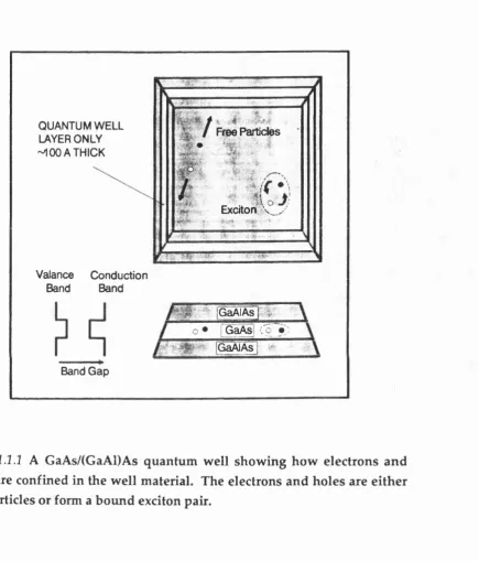
But w hat is a quantum well ? Quantum well m aterial is composed of ultra- thin layers of different semiconductors, typically only 100
A
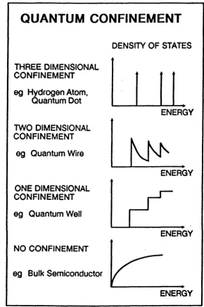
(or about 30 m onolayers) thick, as show n in figure 1.1.1. The materials have different b an d energies and the electrons prefer to remain in the lower gap or well material. H ow ever they are quantum-mechanically confined in the narrow wells, causing fundam ental changes to the density of states in the valence and conduction bands and hence to the shape of the absorption spectra. Figure 1.1.2 illustrates how the density of states is altered as the dim ensionality of the quantum confinement is increased. Full three dim ensional confinem ent gives rise to well defined energy levels as is seen in a hydrogen atom. A quantum well only gives confinement in one dimension an d hence a steplike density of states is seen. The conduction and valence b an d split u p into a series of subbands, the edges of which define the position of the step in the density of states function. The bottom of each subband is at a level equal to the energy level in the one dimensional potential well defined by the conduction or valence band-edges of the two m aterials. There are tw o sets of valence subbands belonging to the heavy and light hole states respectively.•i 4
Free Particles
QUANTUM WELL LAYER ONLY MOO A THICK
w
_ r'\ ^ —
Exciton \_.x
r ,'r i>. rr t,.
•-Valance Conduction Band Band
GaAiAs
GaAs ;'o • •ij£ GaAIAs * Band Gap
QUANTUM CONFINEMENT
THREE DIMENSIONAL CONFINEMENT
eg Hydrogen Atom, Quantum Dot
TWO DIMENSIONAL CONFINEMENT
eg Quantum Wire
ONE DIMENSIONAL CONFINEMENT eg Quantum Well
NO CONFINEMENT
eg Bulk Semiconductor
DENSITY OF STATES
ENERGY
KR
ENERGYENERGY
ENERGY
Figure 1.1.2 The shape o f the density of states function for different degrees of quantum confinement.
c Z
o
KQ.
CC O
</> CD
<
e1 -lh 1
700 750 800 850 900
W A V E L E N G T H ( n m )
Figure 1.1.3 Absorption spectrum of GaAs/(GaAl)As MQWs with
100 A
w ells and
100 A
barriers. Excitonic transitions between the electron (e) and heavy (hh) and light (lh) subband are labelled. Note that the small undulation in absorption longer than the e l-h h l bandedge are spurious and caused by Fabry-Perot effects. Measurement by M.Whitehead.The step-like density of states is dearly evident in the experimental absorption spectrum of figure 1.1.3. However extra transitions are seen just below the edge on each subband. These are exdton states which arise when the electron and hole formed by the absorption of a photon do not have enough energy to escape from one another and hence form a bound state, as illustrated in figure 1.1.1. This state is confined in three dimensions by the coulom b potential and hence has a well defined energy level rather than form ing p art of a continuum. Exdtons are not exdusive to MQW material an d are also form ed in bulk material although quantum confinement shrinks the size of the exdton and hence increases its osdllator strength with the resu lt that they are easily resolved even at room tem perature [Dingle et al., 1974].
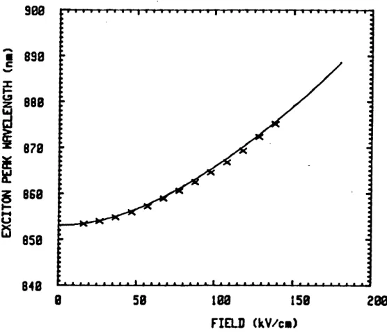
Figure 1.1.4 Illustration of the Stark shift of subband levels in quantum w ells on the application of an electric field.
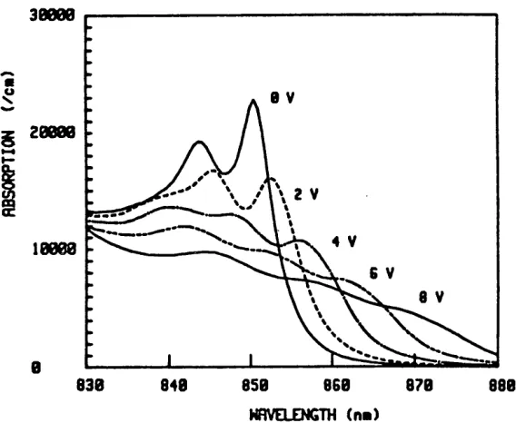
lower energy on the application of an electric field perpendicular to the wells. The size of this shift has been explained [Miller,D.A.B. et al. 1985] by the shifts in the subband energies as the wells become tilted, as show n in figure 1.1.4. But equally im portant is the fact that the exdtons remain, resolvable as they shift because the barriers on either side of the well inhibit field-induced ionization of the exciton and hence prevent the transition broadening through the Heisenberg uncertainty principle. The shift of the exdtons and subband gap can be dearly seen in the absorption spectra show n in figure 1.1.5. Along with the shift, a reduction in the initial transitions osdllator strength and some field enhanced broadening is evident. This field enhanced broadening is caused by inhomogeneous mechanisms linked to interface roughness and variations in field over the wells. As the initially visible transitions subside, initially forbidden transitions grow so that the area under the absorption spectrum stays constant [Miller,D.A.B. et al.,1986]. A model for calculating the absorption spectra will be presented in chapter 2.
c
3 1 k V / c m
m (C
7 9 k V / c m
1 2 7 k V / c m
800 850 900
HflVELENGTH ( n « )
Figure 1.1.5 Field d ep en d en t ab so rp tio n spectrum of GaAs/(GaAl)As M QW s (98
A
wells/111A
barriers) derived from photocurrent m easurem ents on PIN diode. M easurem ent b y M .W hitehead.UGHT IN
GaAs/GaAIAs MQWs
UGHT OUT
In order to apply the electric field over the wells without large currents flowing through the material, the quantum wells are generally incorporated w ithin the intrinsic region of a p-i-n diode structure as illustrated in figure 1.1.6. A sizeable electric field can then be applied by reverse biasing the device. Typical bias dependent transm ission measurements on such a device give the spectra shown in figure 1.1.7. It is interesting to note that this structure is also that of an effective photodiode thus giving important duality of function to the device.
c
0 (0(0
1
(0c
<01.0
o v
B i a s
fa
t r a n s m i t t i n g
II
12V B i a s a b s o r b i n g0.5
0.0
800 850 900
W a v e l e n g t h (nm)
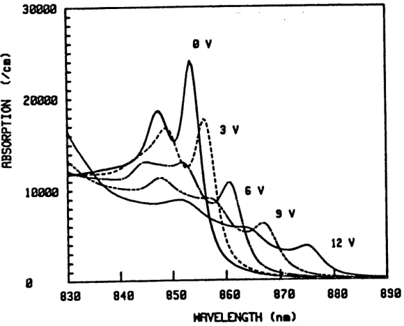
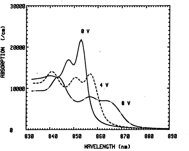
Figure 1.1.7 Transmission spectra on a GaAs/ (GaAl)As MQW p-i-n diode w ith 60 periods of 87
A
w ells and 60A
barriers, for biases of 0,4,8 and 12V. Modulator operates in either a bias absorbing mode at the biased exciton peak or in a bias transmitting mode on the unbiased exciton peak. Measurement by M.Whitehead.Q uantum well m odulators can be m ade in two geometries: with the light travelling parallel to the wells within a waveguide structure [Tarucha et al. 1985, W ood et al. 1985b] and w ith the light propagating perpendicular in the transverse structure [Wood et al. 1984] as illustrated in figure 1.1.8. W aveguide m odulators offer a m uch larger interaction length and hence better m odulation can be obtained. They are particularly suited to integrated optic applications in which other w aveguide components surround them .
i) Transverse
i
n
ii) W aveguide
Figure 1.1.8 Illustration of norm al incidence (transverse) or w aveguide geom etries for MQW modulators.
The principal attraction of the transverse m odulator is the ease w ith which one can couple into it . They are tw o distinct types: non resonant ones w ith anti-reflection coatings on one or both surfaces, or resonant ones with reflections on both surfaces. The non-resonant m odulator is limited in achievable contrast by the thickness of the absorbing region. A reflector on the back surface can change a transmission m odulator to a reflective one w ith twice the optical interaction length [Boyd et al. 1987]. In GaAs/(GaAl)As devices the reflector removes the need to etch away the absorbing substrate.
absorption and therefore increases the transmission: a bias-transmitting mode. These are both illustrated in figure 1.1.7. W aveguide devices are normally only operated in a bias-absorbing m ode because a low value of absorption is required in the high transm ission state so that the insertion loss is kept small.
Q uantum well resonant m odulators were first suggested in high finesse forms whose operation relied upon the electrorefractive shift of the transmission resonance [Guy et al., 1986]. These high finesse m odulators were difficult to grow, and their operation w as very sensitive to environm ental fluctuations as a result of the narrow resonance linewidth. More recently, W hitehead and Parry have proposed and dem onstrated the asymmetric Fabry-Perot modulator (AFPM) [1989a]. Figure 1.1.9 compares the non-resonant reflection m odulator w ith the AFPM. The operation of the AFPM relies upon the destructive interference betw een the front surfaces reflection and the sum of back surface reflections. W ith low absorption in the cavity the back surface reflections dom inate an d a reasonable reflectivity in the on-state is possible. W hen the the absorption is increased one eventually reaches a state in which complete destructive interference can occur w ith a
A nti-R eflectio n
Coating Dielectric reflector
Stacks
Non Resonant AFPM
Figure 1.1.9 Cross sections through a non-resonant reflection m odulator and the AFPM. The AFPM has a front reflection th at destructively interferes w ith the back reflections. At a particular ab so rp tio n in the QW s the overall reflection is zero.
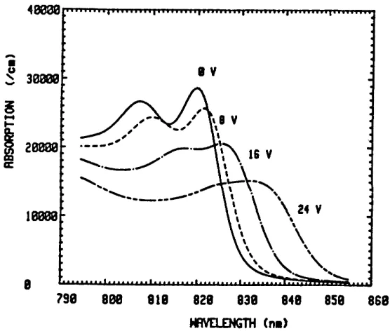
zero reflection output. This gives a theoretically infinite contrast. The operation of the AFPM can be seen in figure 1.1.10, which shows almost zero reflection in the biased state at the resonant wavelength.
In addition to giving very high contrast the AFPM also makes a very effective photodetector, since m ost of the incident light in the zero reflectivity resonant state gets absorbed w ithin the cavity. Thus a high q u an tu m efficiency can be achieved w ithout needing an extensive intrinsic region and the accompanying high reverse bias voltages.
ov
9V
0.8
§
0.66
w
£ 0 4
P4
0.2
0.0
880 870
860 850
840
Wavelength (nm)
Figure 1.1.10 Bias dependent reflection spectra for AFPM device with 75 periods of 95
A
w ells and 60A
barriers w ith front and back reflectivities of 30% and >95%.1.2 Material Systems and their Growth
The realization of the the quantum well m odulator has been m ade possible by som e rem arkable achievements in the grow th of thin layers of Ifl-V sem iconductor material. It is not the purpose of this w ork to describe g ro w th m ethods in detail but it is w orth briefly m entioning the competing techniques used for growing thin semiconductor layers.
intrinsic region. Liquid phase epitaxy (LPE) is a relatively simple technique suitable for the growth of layers not less than 1000
A.
Since the effects of quantum confinement are not really evident until the layer thickness is less than the bulk material exciton radius (*300A
in GaAs), more sophisticated techniques are required for the growth of quantum wells. The two m ost common techniques are molecular beam epitaxy (MBE) [Gossard] and metal- organic vapour-phase epitaxy (MOVPE) [Frijink et al., Roberts et al.]. Both techniques can produce interfaces between layers that are smooth to only a few monolayers. The advantages of MBE have been d te d as sharper interfaces, in-situ RHEED surface analysis and the non-toxicity of the chemicals used. MOVPE however is better able to grow phosphorus containing compounds, and allows rapid source reloading and reprocessing. W hile it is difficult to be certain which of these techniques will be favoured in the future it is reasonable to assume that MOVPE will prove more useful in large scale production whereas MBE m ight be m ore valuable for research. There is also a hybrid technique called gas-source MBE that combines some of the advantages of both MBE and MOVPE.The above techniques are not solely im portant for the manufacture of active optical devices, and somewhat thicker m ultilayers are being grown as optical filters. Most useful of these is the quarter wavelength stack used as a reflector [van der Ziel and Begems, Gourley and Drummond], as it makes possible the fabrication of integrated normal incidence reflective [Boyd et al. 1987] and Fabry-Perot modulators [Whitehead et al. 1989b].
Q uantum wells have been grown in a num ber of material systems and these can be split into two categories : lattice m atched and strained layer systems. In lattice-matched QWs the well and barrier material have the same lattice spacing as the substrate and hence the strain in the materials is relatively small. The m ost developed of all material systems used for QWs is GaA s/(GaA l)A s which operates at wavelengths in the range 800-870 nm. This w avelength is determined by the thickness of the quantum wells, and as will be show n later, this well w idth is also im portant in governing m odulation characteristics. Background dopings of under 1015 cm'3 and interface smoothness of less than a monolayer are now achievable and a clear QCSE has been seen in both MBE- [D.A.B.Miller et al. 1985, W hitehead et al. 1987a] and MOVPE-grown material [Whitehead et al. 1987b]. From a more theoretical viewpoint, this material is also attractive because a consistent set of effective masses and band offsets have been found [R.C.Miller et al.,
Duggan et al.]
However, there is considerable interest in developing other MQW material systems, partly in order to achieve a transparent substrate at the operating wavelength and partly to operate at specific wavelengths such as the 1550 nm optical fibre low loss region. The system which has progressed furthest to date has been (G aIn)A s/InP in which a clear QCSE has recently been seen in a MOVPE grow n sam ple [Bar-Joseph et al., Moseley et al.]. There is, however, an additional uncertainty in the composition of the ternary well material. This complication has delayed a p roper characterisation of the m aterial and there are m any conflicting values for the b an d offsets, effective masses and band nonparabolidties [Forrest et al., Lang et al., Skolnick et al., Sauer et al., Sarkar et al.].
The exciton peak w avelengths for the (G aIn)A s/InP system are in the range 1450-1650 nm , b u t unfortunately, for operation a t 1.55 pm , the well w idth is rather narrow (*70
A)
and large operating voltages are required. This has led to the use of the quaternary system (G aIn)(A sP)/InP so that the band-gap of the well m aterial can be altered w hile retaining a lattice m atch [Zucker et al.].MQW material of (Galn)As wells b u t AlInAs barriers has also been grown, but w ith less success [Wakita et al. 1985] although the reason for this is not yet clear. Encouraging results have also been seen in GaSb/(GaAl)Sb [Miyazawa et al.], but there is even less know n about it, th an (GaIn)A s/InP and it requires grow th on rare GaSb substrates an d the handling of nasty antim ony compounds.
1.3 M odulator Perform ance
The im portant device characteristics are:
i) Degree of Modulation
A n ideal m odulator transm its all of the incident light in its on-state, and absorbs it all in its off-state. In practice this ideal m odulation is not realised and in optim ising the device one m ust choose some figure of m erit to describe the m odulation. Unfortunately, different applications require different figures of merit: some prefer a high on-state, while others require a high contrast ratio betw een the on and off states.
Binary m odulation is fully characterised by the transmission through the device in the on-(Thi) and off-(Ti0) states, as shown in figure 1.3.1. The contrast ratio (Thi/T lo) and m odulation depth ((Thi-Ti0)/Thi) are both often used. In certain application, especially w here optical signals are m erged such as an optical logic gate or telecommunications switch [Ajisawa et al.], a high contrast is a necessity. The problem w ith using it as a figure of m erit is that it can often m ask a very high insertion loss (Thi).
100
% —Thi
-Tlo
-0% _
Figure 13.1 D efinitions for b in ary signal m odulation.
In a sim ple communication system, the single param eter that best describe optim um m odulation is often the transmission change (T^-Tio), as this is directly proportional to the m odulated signal. For a reflection m odulators w e use reflection change.
LAS
J =
0 « ( V ) L
Figure 13.2 Sim ple comm imication lin k w ith M QW diode m odulating lig h t for a laser source w ith signal being detected in a photodetector.
To illustrate this point consider the simple system show n in figure 1.3.2 w here laser light is incident on a modulator, and th e n passed to a simple p-i-n photodetector. The photocurrent generated in the photodetector for transmission T through the m odulator is:
Tlph^
= T|s-m ^lm-r ^las ^ (1.3.1)
he
w here is the laser light output, T|ph the quantum efficiency of the detector, and q m.r are the optical imaging losses from laser to m odulator and m odulator to receiver, X the wavelength, h is Planck's constant, c is the speed of light.
The 'AC' coupled signal is then ^lph^
*s,ac ~ T|s-m ^lm-r ^las AT (1.3.2)
he w here AT is the transmission change
If the receiver noise is dom inated by thermal noise which is the same for the on and off state [Gowar], then the signal to noise ratio is
t1pheA. VR
^s-n ~ Tls-m ^lm-r ^las AT —- (1.3.4)
he V(4kTBw)
w here R is the receiver in p u t resistance, k is Boltzmann's constant, T is the tem perature and Bw is the receiver bandw idth.
The transmission change therefore determines the signal to noise at the receiver. This is supported by the experimental results of Delavaux et al. w ho have m easured the dependence of the receiver bit error rate for changing contrast ratios of a LiNbC>3 m odulator w ith a PINFET receiver.
They analyse their results in term s of a pow er penalty in the receiver caused by the low contrast ratios and this can be well fitted by
Pow er penalty = AT/ T^ (1.3.5)
As one m ight expect, w hen the signal high state power is m ultiplied by the pow er penalty, the result is proportional to the transmission change, hence supporting the use of AT as a figure of merit.
The above calculation is only fully valid for a receiver dom inated by therm al noise as is typical for a p-i-n detector. Avalanche photodiode (APD) receivers will generally be operated in regime where shot noise becomes significant and hence the noise becomes dependent upon the optical power received. The effect of low contrast upon the operation of an avalanche photodetector has been considered by McDonald et al. who show that the further pow er penalty, resulting from using a APD as opposed to a p-i-n, is an order of m agnitude sm aller than the overall one.
ii) Operating Voltage
In order to ease the burden of the driver circuitry, the operating voltage should be as low as possible. Ideally the modulator should be directly driven from standard logic levels, and certainly within the supply rails of the electronic circuitry (typically 5 V or 12 V). It will be shown that the operating voltage determ ines the optim um device thickness and hence the m odulatior performance.
iii) Speed/Capacitance
Liquid crystal and other competing technologies are all of relatively slow speed (except LiNbC>3) com pared to the MQW m odulator and hence speed
is one of the MQW m odulator's strongest selling points. The speed of the device is m ainly determ ined by its p-i-n capacitance and hence scales linearly w ith the m odulator area. Boyd et al. [1989] have recently dem onstrated operation at 5.5 G H z in a 50 pm diam eter device w hen driven by 50Q resistance. One should note however that the driven resistance in some instances will not be so low (eg. *10 k£2 for m inim um size MOSFET), and hence it is im portant to keep the capacitance as low as possible.
iv) Operating Wavelength
This depends upon the m aterial system being used and the well w idth selected. For GaA s/(GaA l)A s it is typically 860 nm.
v) Optical Bandwidth
This is generally related to the linewidth of excitonic absorption peak and is typically 5-10 nm. Typical m ultim oded sem iconductor lasers have a spectral w idth of 3 nm and thus are compatible w ith the m odulator.
vi) Saturation Power
O ne potential problem w ith the MQW electroabsorption m odulators is that the exdton feature being used can be bleached by carriers generated through absorption of the optical power. The density of electron hole pairs generated in a small volum e of QW m aterial is:
N = Ia x /E (1.3.6)
w here I is the intensity,E is the photon energy (1.45 eV), a is the absorption (10000 cm '1), x is the carrier lifetime.
W e estim ate saturation occurs w hen the density of the electron-hole pairs exceeds the density of exdtons ( l/7tL wReX2, w here Lw is the well w idth (100
A)
an d Rex is the ex d to n radius (70A)
) [Chemla et al., 1984]. Thus the saturation intensity isIs = E /2axL w7cReX2 (1.3.7)
because the electric field enhances tunnelling out of the wells [Larsson et al., 1988]. Larsson et al. [1985] m easured photocurrent response times of less than 100 ps. Using this above value we calculate a saturation intensity of 75 kWcm"2, or 75 mW for a 10x10 pm spot size. Boyd et al. [1989] have recently m easured saturation intensities for the same spot size of 3 mW in a high speed reflection modulator. This low value is still unexplained, but it might be related to space charge effects in which the photogenerated carriers tend to screen out the electric field. The topic of carrier escape from quantum wells is one of intense contem porary interest and is likely to provide ways of obtaining operating intensities close to those predicted above.
vii) Temperature Tolerance
The bandedge of MQW m aterial shifts with tem perature and hence the optim um m odulation wavelength changes. We can define two different figures to describe the tem perature tolerance of the modulator. If the source w avelength is fixed, changes of the order of 10 K will have shifted the ex d to n a significant distance aw ay and the modulation will decrease. This is called the fixed w avelength tem perature variation (FWTV). On the other hand if one is able to tune the source wavelength to that of optim um m odulation, a greater tem perature variation can be tolerated. This is the scanning w avelength tem perature variation (SWTV). Although experim ental m easurem ents are still to be m ade it is predicted that the SWTV of an AFPM is smaller than for a non-resonant device because not only does the absorption edge shift, but changes in the cavity refractive index cause a shift of the resonant wavelength. The tem perature tolerance of m odulators will be discussed in more detail in chapter 6, w here the implications for use of the m odulator in an optical interconnect are presented.
viii) Angular Tolerance
A change in m odulation with in d d en t angle for a non-resonant m odulator can a rise from : i) the increased optical path length can actually increase m odulation, and ii), in a very small transmission m odulator, the m odulator w idth can be smaller than the substrate thickness and light can be deflected by the edges of the etched hole in the substrate if the m odulator. Resonant m odulators however are m ore sensitive,
since a change of incident angle also changes the resonant wavelength. At norm al incidence the senstivity to angle is rather sm all and a tolerance of u p to 20° is predicted. Off normal resonance the senstivity is m uch greater, and at 45° the perm itted range is only ±5%. More details can be found in chapter
6.
1.4 Published Modulation Results
There are now a large num ber of published experimental results for electroabsorption modulators. M odulation data for norm al incidence devices are listed in table 1.4.1. These figures should be treated w ith some caution since the insertion losses will tend to vary w ith the experimental arrangem ent. Many of the non-resonant devices have at least one uncoated surface and hence suffer from reflection losses of about 1.5 dB at each interface. Furthermore, even in intentionally non-resonant devices, imperfect anti-reflection coatings can cause Fabry-Perot effects to be visible in the spectrum w hich can change the m odulation by u p to 10%.
The GaAs non-resonant transmission devices show typical operating voltages of 5-10 V, contrasts of 3 dB, and transm ission changes of 30-40%. The results of W hitehead et al. [1988b] indicate the influence of well w idth upon the m odulation. Thin wells give the best transm ission change, but require large voltages, and tend to work in the bias-absorbing mode. Thicker wells operate at low voltages, and normally in a bias-transm itting mode. Hsu et al. achieve a contrast of 10 in the bias-transmitting m ode by making a much thicker device. Unfortunately, along with the 10 dB contrast they get a 13 dB insertion loss and require an operating voltage of 20 V.
We can compare the MQW results with those of W ight et al. for bulk GaAs m odulators utilising the Franz-Keldysh effect. Because the changes of absorption are m uch smaller in these materials, the insertion loss is generally high (8.2 dB) and the m odulation limited (1.1 dB).
Group Well N um ber Width of wells
A
Contrast Ratio
dB
Insertion Loss
dB
Transmission Volts Speed Change
% V ps
GaAs Transmission
Wood et al, 1984 95 50 2.83 1.87 -35 8
Wood et al, 1985a 95 50 2.19 1.19 -32 9 <131
Whitehead et al, 1988b
47 75 2.8 1.8 -36 20
Whitehead et al, 1988b
87 60 3.4 3.1 -27 12
Whitehead et al, 1988b
147 45 2.5 2.67 24 12
Hsu et al, 1988a 100 200 10 13 5 20
Bulk GaAs Transmission
Wight et al, 1985 1.1 8.2 3.5 5
Non-resonant Reflection
Boyd et al,1987 97 65 9.0 6.0 -22 18 29
AFPM
Whitehead et al 1989c
95 75 20 3.5 -42.6 9
AFPM on Silicon
Barnes et al.,1989 120 75 1.45 2.22 -17 8
(Galn)As Transmission
Koren et al,1987a 100 100 0.97 4.56 -7 20 30
Wakita et al,1985 75 60 0.93 ? ? 20
Guy et al, 1989 100 150 2.4 2.8 -40 40
Table 1.4.1 Performance of norm al incidence electro-absorption m odulators.
W aveguide results are presented in table 1.4.2. In w aveguides the coupling losses are often large and will vary depending on the optics used. The longer, unconstrained, interaction length possible in a w aveguide makes very
h ig h contrasts possible, independent of w hether the m aterial is GaAs or (Gain)As or even bulk material [Noda,Y. et al].
In this section w e have concentrated u pon the use of MQW diodes as m odulators, although w e have already m entioned that they make
good photodetectors as well. The response time of the device as a
detector is bias-dependent and has been investigated by Larsson et al. [1985]. R esponse times of typically 100 ps were observed indicating that very high sp eed operation is also possible as a photodetector.
G roup Well Number Contrast Insertion Transmission Volts Speed Width of wells Ratio Loss Difference
A dB dB % V ps
GaAs W aveguide
Wood et a l, 1985b 97 2 10 7.21 -17 15 97
Tarucha et al.,1985 18 16 3.01 7 ? 1.4 350
(Galn)As Waveguide
Wakita et al,1987a 67 10 8.86 13 -13 1.8
WaJdta et al,1987a 67 40 15 12 -6.1 9 160
Koren et al,1987b 80 80 18.7 2.7 -50 20 53
Bulk (Galn)As Waveguide
Noda,Y., et al, 1986 23 9.6 -10.9 11 41
Strained Layer (Galn)AsZGaAs
Das e ta l,1987 100 64 1.21 0.91 -20 9 150
GaAs Coupled Wells
Islam et a l,1988 47.5 4 11.4 ? ? 3.5
1.5 Sum m ary
In this chapter we have described the MQW electroabsorption m odulator and its operation. It can be manufactured in a num ber of different material systems, b u t GaAs/(GaAl)As is much the most developed and understood. We have then defined and estimated what are the device's m ost im portant properties. In describing the modulation we have introduced the use of transmission change to describe the modulation, especially in simple communication links w here it reflects the 'AC' m odulation on the light signal. Finally we have m ade a survey of data from published devices. From this collected data, w e find that non-resonant transverse devices operating at low voltages and low insertion losses have limited contrasts and w aveguide devices offer high contrasts, but with associated difficulties of coupling into the guide. On the other hand the recently proposed and dem onstrated AFPM seems to offer high contrast, low insertion loss operation at reasonable voltages.
As described in the preceding chapter, the quantum well electroabsorption m odulator utilises the large changes of absorption on the application of an electric field perpendicular to the wells. The first step in optim ising the device m ust therefore be the understanding and m odelling o f this basic electroabsorption effect.
The dom inant features at the band edge are transitions between the conduction and valence n = l subbands and their associated exdtons. Miller,D.A.B. et al. [1985] was the first to consider the changes in absorption arising from the application of an electric field. In the direction parallel to the wells, it was found that the exdton broadened rapidly due to ionisation in the applied electric field. How ever, a qualitatively different effect is seen for a perpendicular field w here the barriers prevent field ionisation. The ex d to n s therefore remain resolved at high fields and a d ear Stark shift to low er energy is seen. Accompanying this shift one also gets a reduction in oscillator strength and additional inhom ogeneous broadening. The shift has been m odelled by m any authors [Miller,D.A.B. et al. 1985, Fernandez and C astro, Bastard et al., Austin and Jaros, M atsuura and Kamizato, Singh and H ong, H arw it et al.] and nam ed the Q uantum Confined Stark Effect (QCSE). The reduction in the ex d to n 's oscillator strength has been successfully related to the overlap integral betw een the electron and the hole wavefunctions [Miller,D.A.B. et al. 1986]. A num ber of broadening m echanism s in a practical m odulator have been proposed : lifetime broadening due to tunnelling through the barriers and phonon interaction, inhom ogeneous broadening caused by well w idth fluctuation [Juang et al.] an d electric field variations from well to well d u e to background doping in the intrinsic region [Newson and Kurobe].
Several authors had used calculations of the subband energies to evaluate a theoretical absorption spectrum [Sanders and Bajaj, Klipstein and Apsley, Ikonic et al.], b u t to m y knowledge no one has previously in d u d e d both the loss in osdllator strength and the effects of the inhom ogeneous broadening mechanisms described above, and m ade com parisons w ith experimental data.
In this chapter w e develop such a m odel for GaAs/(GaAl)As material.
2.2 Evaluation of Subband Energies
M ultiple quantum well material has, b y definition, barriers of such a w idth that coupling between wells is unim portant so that the electronic states of the material are characterised by those of the single well. A relatively simple theory to describe the electronic states of a quantum well has been developed in the last few years. This theory is been based on the envelope approximation in which the wavefunction is split into the Bloch states and an envelope function that spatially m odulates the Bloch states [Bastard and Brum]. Once the band edges and the effective masses describing the Bloch states of the com ponent materials have been determ ined, the envelope function is relatively easily calculated as a result of the simplicity of geometry of the well structure.
It is found that the component of electron m om entum perpendicular to the wells is quantised and as a result the valence and conduction bands are split into a series of subbands. W ithin each subband the electrons are only free in two dimensions and this restriction causes the density of states function to have a step-like shape at the band edge. The quantum confinement also lifts the degeneracy of the valence band and leads to the observation of two sets of subband transitions, nam ely the heavy and the light hole.
The edges of the subbands described above are equal to the energy levels in the one dimensional well defined by the alignm ent of the band- edges in the tw o component materials. In a perpendicular electric field, these wells tilt and the energy level changes w ith respect to the centre of the well. This change is the origin of the QCSE. The shift has been m odelled perturbatively [Fernandez and Castro], using variational m ethods [Bastard et al.], using exact Airy function solutions [Austin and Jaros, M atsuura and Kamizato], and by Monte Carlo [Singh an d Hong] and tunnelling resonance methods [Miller,D.A.B. et al 1985, H arw it et al.].
Figure 2.2.1 Resonant tunnelling barrier used to determine energy levels in a finite potential w ell in an electric field. Typically 20 steps are used in each layer.
continuously sloping potentials; ii) the tunnelling through the finite barriers is also modelled; iii) the non-parabolidty of the bands can be taken into account when calculating the w avenum ber in each step; iv) the electron- hole overlap integral can be easily calculated from the values of the wavefunction evaluated in each step.
W ithin each step the envelope-function is assum ed to be the combination of a forward and a reverse travelling w ave or their evanescent equivalents:
f(z) = A exp(ikz) + B exp(-ikz) (2.2.1)
w here f is the envelope-function, A and B arbitrary constants and k the wavenumber. The w avenum ber is
k = 2ji[2mL’(E - V(z))]1/2/ h (2.Z2)
w here E is the particle energy, h is Planck's constant, V, the potential and mj_* the effective mass perpendicular to the wells.
Two easily applicable m ethods have been proposed to account for nonparabolic bands by H iroshim a and Lang and Nelson et al. [1987a]. The energy dependent effective m ass approach [Hiroshima and Lang] has been
chosen since it includes the nonparabolidty of the barrier m aterial and the effects of nonparabolidty on the boundary conditions at the interface. The energy dependent effective masses used for the electron and the light hole are given by
m /(E ) = m / [ l + (E - V(z)) / Enp] (2.2.3)
w here Enp = h2/87c2m 1*Y (2.2.4)
w here y is the band nonparabolidty. The calculation of the transmission coefficient is m ade by using a transfer matrix to evaluate the wavefunction throughout the structure. The mathematics is exactly the same as that used to calculate the optical transmission through a series of dielectric layers of differing refractive indices [Bom and Wolf]. At any interface the value of the envelope wavefunction itself (f) and (l/m *)3f/5z are conserved [Bastard and Brum]. A transfer matrix is then used to relate the values of the f and (1 / m )df / dz on either side of a potential step:
(
f
^
^ c o s ( k A z ) ( m / k ) s i n ( k A z ) ^f f >1
^(1 / m * ) 3f / 3 z y ^ (k / m ) sin ( kA z) c o s ( k A z )
u
/ m x) S f / 9 z y(2.2.5) w here Az is the width of the step.
ELECTRON
LIGHT HOLE
-IB
HERVY HOLE
Ui
-20
-30
-40
150
100
50
0
FIELD (kV /ca)
Figure 2.2.2 Energy level of the n = l electron, heavy an d lig h t hole su b b an d s as a function of electric field. The w ell w idth is
100 A
and the barriers are of 30 % alum inium .band non-parabolicity is found to have a m inor effect of the zero-field subband energy, but very little difference is seen in the shift. Negative subband energies are possible at high fields because the energy level is m easured with respect to the potential of the m iddle of the well, significantly above the bottom comer of the well w hen the electric field is applied.
Before calculating the transition energies between conduction and valence subbands, one more item m ust be addressed: the effect of stress in the well material. Miller,D.A.B. et al. [1985] suggest that the difference in lattice constant for the GaAs (5.6533
A)
and the (GaAl)As (5.6564A)
gives rise to a strain in the sample that shifts the light hole subbands. One m ight expect the larger bulk of the GaAs substrate to determ ine the lattice constant in the wells and since the wells are also GaAs there should be no strain shift. How ever there is evidence that during growth, the formation of lattice interface dislocations relieves the strain in the (GaAl)As buffer and barrier regions, at the same time introducing it into the GaAs wells [Dingle and Wiegmann]. We find that a consistent split between the light and heavyhole ex d to n s (sample I) w hen w e assum e a stress of 47 M N /m 2 present in the GaAs, a value suggesting the stress is equally shared between well and barrier material. This causes shifts of -0.25 and 3.2 meV for the heavy and light holes respectively.
The subband gap for both the heavy and light hole subbands is the sum of the bulk well material band gap (Eg), the m th electron (Ecm) and the nth hole (Ey11) subband levels, and the strain shift ( Estm):
Ecvm'n(F) = Eg + Ecm(F) + Eyn(F) - Estrn (2.2.6)
w here F is the electric field.
The effective masses [Miller,RC. et al.], bandgaps [Casey and Panish], ban d offset ratios [Duggan et al.] and nonparabolidty parameters [ Nelson et
al., 1987a] used for the GaAs/(GaAl)As are show n in table 2.2.1.
Param eter Value
Electron m ass (mo) 0.0667 + 0.0835x
H eavy Hole Mass (mo) 0.34 + 0.412x
Light Hole Mass (mo) 0.094 + 0.066x
Bandgap (eV) 1.4247 + 1.247x
Band Offset Ratio (%) 65
Electron N onparabolidty (m2) 4.9 x 10'19 Light H ole N onparabolidty (m2) 7.35 x 10"19
Table 2.2.1 List of param eters of (GaAl)As used in the calculations of the su b b a n d energies of MQWs. The assum ed tem perature is 295 K and X is the alu m in iu m m ole fraction.
The tunnelling resonance technique also provides values of the w avefunction through the well and the surrounding barriers. Numerical integration can then be used to calculate the electron-hole overlap integral:
Mcvm,n = | fcm(z)fv"(z)*dz | (2.2.7)
w here fcm and fvn are the mth conduction and n th valence subband envelope w avefunctions respectively.
.5 o
tn
288 158
188
FIELD (k V /ca)
Figure 2.23 The square of th e overlap integral betw een the electron and hole w avefunctions as a function of perpendicular electric field. The calculation is for 100
A
w ells and 60A
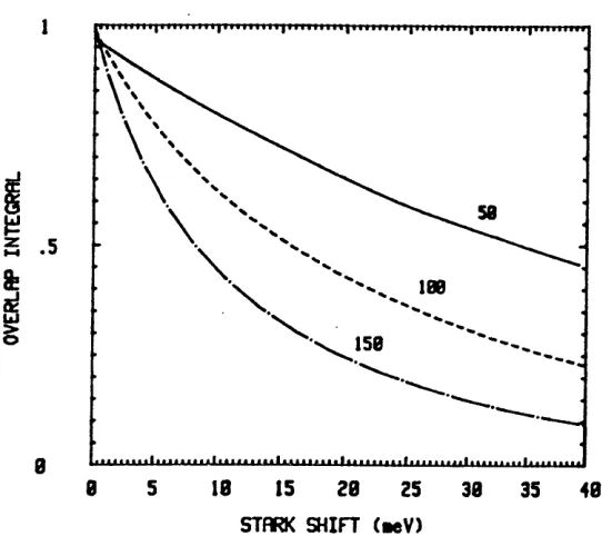
barriers and a barrier alum inium concentration of 30%.barriers. The oscillator strength is proportional to the square of the overlap integral [Miller,D.A.B. et al. 1986]. Figure 2.2.3 plots the square of the overlap intergral as a function of electric field for the n= l heavy hole to m = l electron (el-h h l), n = l light hole to m = l electron (el-lhl) and n=2 heavy hole to m = l electron (ell-hh2) transitions. The wavefunctions for transitions w ith differing subband num bers, are almost orthogonal to one another at zero field and are called forbidden transitions because of the sm all initial overlap. On the application of an electric field the initially allow ed transitions' oscillator strengths subside, whereas the forbidden transitions grow. This is clearly seen in figure 2.2.3 where the e l-h h l and e l-lh l transition subside and the el-hh2 transition grows.
The w idth of the tunnelling resonance is related to the tunnelling through the barriers by the Heisenberg uncertainty principle. The linewidth o f the electron, heavy and light hole are show n in figure 2.2.4 and it can be seen th at u p to 150 kV /cm they do not e x c e e d 1 m eV.
if
* 10"*
10
10H
10H
10
10
r?
LIGHT HOLE
ELECTRON
HEflVY HOLE
0 50 100 150 200
FIELD (k V /c a)
Figure 2.2.4 The variation of the tunnelling resonance line w idth with electric field for electron (middle), and light (upper) and heavy hole (lower) n = l levels. The calculation is for 100
A
w ells and 60A
barriers and a barrier aluminium concentration of 30%.2.3 Determination of Well Widths
A n assessment of the well w idths of quantum well devices is a natural prerequisite for modelling their physical characteristics since the Stark shift is sensitively dependent u p o n it.
diffraction (XRD) or transmission electron m iscroscopy (TEM). Of these PLE and XRD are the m ost reliable and good agreem ent betw een the various methods has been found [Orton et al.]. H ow ever, there is still a possibility that the grow th rates over the wafer can vary, an d hence the assessment of the well w idth of a particular device is best derived from m easurements taken on that device.
Fortunately, the presence of well defined ex d to n transitions in the absorption spectra allows us to do just that. W e have already m entioned these exciton transitions as being states created w ith photon energies just below the subband separation energy and arising from the m utual attraction betw een the exdted electron and hole. The transition energy is given by
Eex = Ecvm'n -E b (2.3.1)
w here Eb is the binding energy. Calculation of the binding energy of a quantum well exciton w as first done by Greene et al., and subsequently by m any authors [Miller,D.A.B. et al. 1985, Ekenberg and Altarelli, N elson et al.,1987b]. The well w idth dependence of the binding energy is im portant and for our calculations w e use the results of Ekenberg and Altarelli w ith the following fit (in meV):
Ebhh = 14.2 - 0.0705 L „ + 1.75X10"4 L„2 (2.3.2)
Ebm = 16.1-0.061 Lw + lO-’ Lw2 (2.3.3)
w here Lw is the well w idth. We neglect the small variation of Eb w ith barrier aluminium concentration.
Figure 2.3.1 shows the variation of the exdtonic peak as a function of the QW thickness. The estim ates obtained from this graph have been found to be reliable and have been used in recalibrating the MOCVD grow th kit at Sheffield University which had earlier routinely produced w ell thicknesses less than those spedfied.
« 880
■
c w 870
860
850
840
S 830
H
2 820
810
800
790
0 50 100 150 200 250
HELL WIDTH (A)
Figure 2.3.1 Exciton w avelength for e l- h h l tran sitio n against well w idth, for barrier alum inium concentrations of 30 % (solid) and 40 % (dashed). The tem perature is 297 K.
2.4 Calculation of A bsorption Spectra
Calculations of the absorption spectra near to the band edge have been published by several authors: an empirical m odel using tw o Gaussians for the heavy and light hole exdtons and a single continuum has been proposed by Chemla et al. [1984] and several models derived from m ore fundam ental calculations of the band structure [Sanders and Bajaj, Klipstein and Apsley, Ikonic et al.]. However none of them model the field dependent broadening m echanisms necessary to give good agreement w ith experimental results.
transitions to exdtonic states just below the subband gap energy.
The unbroadened contribution from each pair of subbands can be w ritten as the sum of a delta function to describe the exciton and a step function, m ultiplied by the Sommerfeld factor for the continuum:
“ hh/lh™'" = o -M m'ncv2(F) { fex5[E-Ecvm'n(F)+Eb] (2.4.1) + H[E-Ecvm,n(F)] S[E/Ecvm,n(F)] )
w here E is the photon energy, F the electric field, a * the absorption of the continuum , Mcvm'n the overlap integral betw een the electron and hole wavefuctions, fex the relative strength of the exciton to the continuum , 8[E] the Dirac delta function which describes the unbroadened exciton,
the field-dependent separation between the n = l electron and hole subbands, Et, the exciton binding energy, H[E] the Heaviside step function and S[E,Ecv] the Sommerfeld factor.
Equation (2.4.1) is similar to that used by Klipstein and Apsley. The heavy and light hole states are uncoupled and only a single IS exciton state is included. Dawson et al. [1986] have observed a 2S exciton state, but only w ith a good sample at low temperatures using PLE. Theory predicts th at its strength is 1/27 of that of the IS state, and both it and higher states can be included in the calculation. The following other features are added that m ake ou r calculation different from that of Klipstein and Apsley : the oscillator strengths for the two transitions considered are proportional to the square of the overlap integral between the electron and the hole envelope functions, a Sommerfeld factor is included in the shape of the continuum , and further inhomogeneous broadening is accounted for by successive convolution w ith the appropriate lineshape.
The Sommerfeld factor is an enhancement of the free particle subband absorption around the band edge because of the Coulomb attraction betw een the electron and hole, and for a two-dimensional exciton it was first calculated by Shinada and Sugano and is given by
SfoEcv111'11] = (2.4.2)
1 +exp[-2jtRy1/2/(E-Ecvm'n)1/2]
w here Ry is the Rydberg constant: e V
8e2h
w ith p. the red u ced mass of the exciton:
Ry = z \ (2.4.3)
3 « 2u 2
m | l c m | l v
^ ;--- . (2.4.4)
m ||c + m | | v
and e is the electronic charge, e the perm ittivity of MQW material which is assum ed to be m idw ay between those of the well and barrier material and m 11 c* an d m ||v* are the effective masses of the electron and hole parallel to
the plane of the well. The heavy and light hole masses differ from their values in the perpendicular direction and are given by [Chemla and Miller, 1987]:
4m_Lhh m_Qh
m m * «---;---. (2.4.5)
3m_Lhh +mjjh
4m_Lhh* mjjh*
m lll h = --- ;---, (2.4.6)
m J_hh + 3 m j j h
The relative oscillator strengths for the heavy and light hole transitions d ep en d u p o n the polarisation of the light. W hen the light is propagating p erpendicular to the well, the electric field vector is always directed in p lan e of the QW. On the other hand w hen the light is propagating parallel to the QW s, the electric field can either be parallel or perpendicular to the QW s, ie. the transverse electric (TE) and transverse magnetic (TM) modes. The com bination of states excited in the quantum well depends upon the direction of electric field. In the TM m ode the heavy hole is completely su p p ressed at the band edge whereas in the TE m ode the ratio between the oscillator strengths for the heavy and light hole contribution is 3 to 1 [Asada et al.,Yamanishi and Suemune] and hence the absorption coefficient for the stru ctu re as a whole is given by
ocqw= I I (Xhhm,n + (1/3) I I a lhm'n (2.4.7)
* in n m n
independent of the barrier thickness. The absorption coefficient for the composite material is given by
= [Lw/ (Lfc+Lw)] ctq^v (2.4.8)
w here Lw and Lb are the well and barrier w idths respectively.
■
o \ 3
cn
OQ
a:
z 5000
M *—
3 U
0 50 100 150 200 250
HELL HIDTH (A)
Figure 2.4.1 V alues of heavy hole continuum (cO derived from experim ental spectra w ith em pirical fit (solid) to the data. T he dotted line is a 1/Lvy.
We define as the absorption in the heavy hole continuum. N ote that to relate it to the continuum absorption m easured at wavelengths just shorter than the light hole exciton, one needs to multiply by 4 /3 to include the light hole contribution and then by 1.8-1.9 for the Sommerfeld factor. In order to achieve the most realistic results from the modelling w e have derived <x» from experimental results over a range of well w idths. This was done by curve fitting from spectra supplied by Jelley et al., and the result can be seen in figure 2.4.1. An empirical fit to the data is given by
Also plotted in figure 2.4.1 in the dotted line is the inversely proportional relationship, equivalent to a constant absorption per well. This is predicted by simple theory [Matsumoto et al.].
€ 20 £
u
8 10
200 250
150
50 100
HELL HIDTH (R)
Figure 2.4.2 V alues of relative exciton area (fex) derived from experim ental spectra w ith em pirical fit to the data.
In addition to the continuum level w e also derive the relative e x d t on area (fex) from experimental spectra. N ote that by area w e m ean the area u nder the absorption spectra, not the ex d to n 's spatial extent. It is convenient to define fex in terms of the Rydberg constant since theoretical calculations predict fex = 16 Ry for a 2D ex d to n [Shinada and Sugano, Chemla et al., 1985]. In figure 2.4.2 w e plot the experimentally-derived results with the following empirical fit:
fex = 22 - 0.105LW + 2x10'4Lw2 (2.4.10)
dimensional case. However, since the Sommerfeld factor tails off slowly w ith increasing energy, provided one is only interested in photon energies around the b an d edge, it can be regarded as alm ost constant and the resultant lower f ^ is cancelled by a higher
U nder the application of an electric field w e assum e th at both the relative area and the binding energy of the exciton rem ains constant. Thus the exciton decays w ith the continuum, dependent u p o n the electron-hole wavefunction overlap. This assumes that the lateral extent of the exciton does not change, although in practice it is likely to increase slightly as a result of the increased separation of the electron and hole. As for the binding energy, a variational calculation by Miller,D.A.B. et al. [1985] has estim ated that there is a drop in binding energy of about 2.5 meV for a well of 95
A
in a field of 120 kV /cm , which is an order of m agnitude lower than the overall shift of 25 meV. Two other authors [Sanders and Bajaj, Brum and Bastard] have perform ed similar calculations and observe a similar reduction although they do not show results at high fields.2.5 B roadening Mechanisms
Expression (2.4.1) includes delta- and step-functions which are not practically realisable. This is because broadening of the spectra take place through a num ber of mechanisms which are accounted for by successive convolution with the appropriate lineshape.
i) Phonon Broadening
Any exciton created by the absorption of a photon has a finite lifetime, which will cause a broadening in the transition energy through Heisenberg's uncertainty principle. Possible mechanisms for the destruction of an exciton are recombination, tunnelling of either the electron or hole through the barrier, and phonon interaction. Chemla and Miller [1985] have shown that it takes only 300 fs for exdtons to be ionised by phonons at room temperature, m uch shorter than the nanosecond timescale over which recombination takes place [Dawson et al.,1985, M atsusue and Sakaki]. The tunnelling rate through the barriers is dependent upon the composition and w idth of the barriers and can be calculated from the w idth of the tunnelling resonance found w hen calculating the subband energy. As shown in figure 2.2.4, with 60
A
barriers of 30 % alum inium concentration, at all fields of interest this broadening is less than 1 meV and can be neglected. Thus, phonon broadening is generally the dom inant homogeneous broadening mechanism.Chemla et al. [1984] have proposed that the tem perature dependence of the phonon broadening is proportional to density of LO phonons, described by the Bose-Einstein distribution:
^ph
rT
= --- —--- (2.5.1) [exp(hQLO/kT)-l]w here P f is the full width half maximum (FWHM) linewidth, k is Boltzmann's constant, T is the tem perature and Qlo is the LO phonon energy (37 meV).
is
>
I
O
0 ... I
0 50 100 150 200 250 300 350
TEMPERATURE (K)
Figure 2.5.1 H eavy hole exciton linew idth m easured from photocurrent data over a range of tem perature. Fitted line is calculated b y convolution of a L orentzian to describe the phonon broadening, w ith G aussian an d sq u are ones for the w ell w idth fluctuation and background doping m echanism s respectively. Experimental data was m easured by M .W hitehead an d P.Dobson on m aterial grow n at Philips Research b y K. W oodbridge
(sam ple I) as a function of tem perature [Whitehead, Dobson and W oodbridge, unpublished]. The fitted line is obtained by convolution of the low tem perature broadening with that of the phonon broadening w ith r ph = 20.5 meV. This value is larger than that reported by Chemla et al. [1984] (11 meV) since w e have assumed a convolution of different lineshapes rather than a simple addition. It is very close to the independent estimate of 20.7 meV by C hen et al. w ho use a similar technique.
The rate of phonon scattering is assumed to be independent of applied field. A lthough w e can give no absolute justification for this, the LO phonon energy is m uch greater than the exciton binding energy and thus any collision betw een a phonon and an exciton is likely to ionise the exciton [Chemla et al.].