Mixed Radix Design Flow for Security
Applications
A.Rafiev
Technical Report Series
NCL-EECE-MSD-TR-2011-175
Supported by EPSRC grant GR/F016786/1
NCL-EECE-MSD-TR-2011-175
Copyright c2011 Newcastle University
School of Electrical, Electronic & Computer Engineering, Merz Court,
Newcastle University,
Newcastle upon Tyne, NE1 7RU, UK http://async.org.uk/
The purpose of secure devices, such as smartcards, is to protect sensitive information against software and hardware attacks. Implementation of the appropriate protection techniques often implies non-standard methods that are not supported by the conven-tional design tools. In the recent decade the designers of secure devices have been working hard on customising the workflow. The presented research aims at collect-ing the up-to-date experiences in this area and create a generic approach to the secure design flow that can be used as guidance by engineers.
Well-known countermeasures to hardware attacks imply the use of specific signal encodings. Therefore, multi-valued logic has been considered as a primary aspect of the secure design. The choice of radix is crucial for multi-valued logic synthesis. Prac-tical examples reveal that it is not always possible to find the optimal radix when taking into account actual physical parameters of multi-valued operations. In other words, each radix has its advantages and disadvantages. Our proposal is to synthesise logic in different radices, so it could benefit from their combination.
With respect to the design opportunities of the existing tools and the possibilities of developing new tools that would fill the gaps in the flow, two distinct design ap-proaches have been formed: conversion driven design and pre-synthesis.
The conversion driven design approach takes the outputs of mature and time-proven electronic design automation (EDA) synthesis tools to generate mixed radix datapath circuits in an endeavour to investigate the added relative advantages or dis-advantages. An algorithm underpinning the approach is presented and formally de-scribed together with secure gate-level implementations. The obtained results are re-ported showing an increase in power consumption, thus giving further motivation for the second approach.
The pre-synthesis approach is aimed at improving the efficiency by using multi-valued logic synthesis techniques to produce an abstract component-level circuit before mapping it into technology libary. Reed-Muller expansions over Galois field arithmetic have been chosen as a theoretical foundation for this approach. In order to enable the combination of radices at the mathematical level, the multi-valued Reed-Muller expansions have been developed into mixed radix Reed-Muller expansions. The goals of the work is to estimate the potential of the new approach and to analyse its impact on circuit parameters down to the level of physical gates. The benchmark results show the approach extends the search space for optimisation and provides information on how the implemented functions are related to different radices.
The theory of two-level radix models and corresponding computation methods are the primary theoretical contribution. It has been implemented in RMMixed tool and interfaced to the standard EDA tools to form a complete security-aware design flow.
First of all, I would like to thank my mother, Nina, for her love and patience. Even from far away she has been supporting me every day.
I am very grateful to my supervisors, Alex Yakovlev and Albert Koelmans. I would have never been able to succeed in my research without their help and guidance. Also many thanks to my friends and colleagues – Andrey Mokhov, Arseniy Alekseyev, Julian Murphy, Frank Burns, Danil Sokolov, Stanislavs Golubcovs, and Ivan Poliakov – for many useful and inspiring ideas, criticism, support, and for just being very nice. I kindly thank Michael Keller and Anne Harrow for the spiritual support and
encouragement they have been giving me throughout these years.
This research was supported by the EPSRC grant GR/F016786/1 (SURE) and the ORS Awards Scheme.
Abstract 1 Acknowledgements 2 List of Figures 6 List of Tables 8 List of Publications 10 1 Introduction 1 1.1 Motivation . . . 3 1.2 Contribution . . . 7
1.3 Organisation of the thesis . . . 9
2 Background 12 2.1 Hardware Attacks and Countermeasures . . . 12
2.1.1 Types of attacks and countermeasures . . . 12
2.1.2 Power balancing using m-of-n codes . . . 15
2.2 Galois Fields and Reed-Muller Expansions . . . 23
2.2.1 Galois Fields . . . 23
2.2.2 Multi-valued Reed-Muller expansions . . . 32
2.2.3 Green’s direct method . . . 33
3 Baseline Research 41
3.1 Secure Design Flow . . . 41
3.1.1 Data path synthesis . . . 42
3.1.2 Control path synthesis . . . 45
3.1.3 Physical design . . . 48
3.2 Conversion Driven Mixed Radix Design . . . 49
3.2.1 Conversion basics . . . 49
3.2.2 Types of gate grouping . . . 51
3.2.3 Grouping based on bitwise regularity . . . 54
3.2.4 Grouping based on binary trees . . . 58
3.2.5 Component implementation . . . 61
3.2.6 Benchmark results . . . 64
3.3 Summary . . . 66
4 Mixed Radix Reed-Muller Expansions 69 4.1 Two-level mixed radix model . . . 69
4.2 Radix reduction:pt →pu,t > uReed-Muller expansions . . . 72
4.3 Radix extension:p→ptReed-Muller expansions . . . 79
4.4 Mixed radix domain: p,pt →ptReed-Muller expansions . . . 85
4.5 Binary-to-q-nary Reed-Muller Expansions . . . 90
4.6 Summary . . . 96
5 Use Case and Experimental Results 98 5.1 Component implementations . . . 99
5.1.1 Implementation using RTL . . . 99
5.1.2 Dynamic logic implementation . . . 104
5.1.3 Estimating component physical parameters . . . 105
5.2 Mapping specifications from one radix to another . . . 108
5.3 Synthesis tool and optimisations . . . 110
5.5 Summary . . . 124
6 Conclusion 126 6.1 Future work . . . 128
A RMMixed User Manual 130 A.1 Tool features overview . . . 130
A.2 Command line tool: rmmixed-cmd . . . 131
A.3 Galois field expression calculator . . . 133
A.4 List of Tcl commands . . . 135
A.5 Workflow example . . . 155
1.1 Understanding the difference between general purpose MVL and
application-driven MVL synthesis flows . . . 5
1.2 Thesis flowchart . . . 10
2.1 Types of cryptanalysis . . . 13
2.2 Switching activity in CMOS inverter . . . 16
2.3 CMOS NAND gate . . . 17
2.4 Dual-rail (1-of-2) protocol . . . 18
2.5 4-phase handshake . . . 19
2.6 RTL implementions of dual-rail encoded AND gate showing different levels of power balancing. . . 20
2.7 Power signatures for different data transitions illustrating the imbalance. 21 2.8 Power signatures (overlayed) . . . 21
2.9 Addition and multiplication of{[0],[1],[x],[x+1]} . . . 28
2.10 Addition and multiplication over some finite fields . . . 30
2.11 Binary RM expansion, component-level schematic. . . 38
2.12 Component-level schematic for uniform radix (quaternary) RM expansion. 40 3.1 CDD-based design flow . . . 44
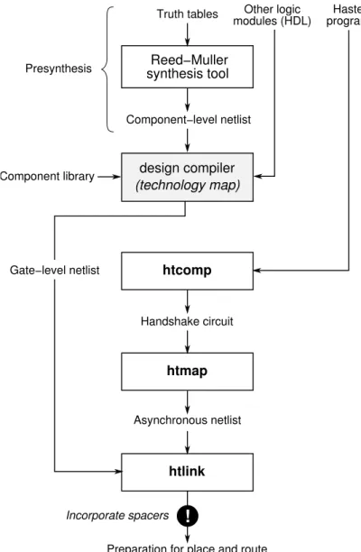
3.2 Reed-Muller + Haste synthesis flow . . . 46
3.3 Example of a binary circuit that cannot be efficiently converted into a higher radix circuit. . . 50
3.4 Mixed radix circuit as a result of binary-to-q-nary conversion. . . 51
3.5 Types of gate groupings (considering the same original circuit). . . 52
3.6 Understanding Q/B gates. . . 53
3.7 Mixed radix circuit using Q/B gates . . . 53
3.8 Example original single-rail circuit: 2-bit adder. . . 57
3.9 2-bit adder converted using bitwise regularity approach; gates are shown as “black boxes”. . . 57
3.10 2-bit adder converted using binary trees approach; gates are shown as “black boxes”. . . 61
3.11 SPICE simulation results for AES S-box showing supply current, mA. . . 67
4.1 Mixed radix circuit based onq1→q2two-level radix model. . . 72
4.2 r2(x) +r2(y)component specification for quaternary-to-binary case . . 77
4.3 Component-level schematic for quaternary-to-binary RM expansion. . . 78
4.4 Component-level schematic for mixed radix binary-to-quaternary RM expansion. . . 85
4.5 Component-level schematic for mixed-to-quaternary RM expansions. . . 90
4.6 Component-level schematic for binary-to-ternary RM expansion. . . 96
5.1 Dual-rail encoded GF(2) addition . . . 100
5.2 1-of-4 encoded GF(4) addition . . . 101
5.3 1-of-4 encoded GF(4) multiplication, relaxed balancing . . . 102
5.4 1-of-4 encoded GF(4) multiplication, fully balanced . . . 103
5.5 Dynamic logic implementation of 1-of-4 encoded GF(4) addition . . . 104
5.6 “Wire crossing” operations in 1-of-4: their implementations do not involve any logic . . . 107
5.7 An example of using therepetitionheuristics to handle “don’t care” values.109 5.8 Reed-Muller based synthesis flow . . . 111
2.1 Encoded binary, ternary and quaternary signals. . . 19
2.2 Dual-rail AND gate truth table and its single-rail equivalence . . . 20
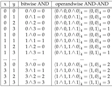
3.1 Bitwise and operandwise quaternary operations example . . . 53
3.2 Inversion in 1-of-4 . . . 64
3.3 Single rail circuits converted to dual-rail . . . 65
3.4 Mixed radix conversion results . . . 66
5.1 GF component implementations . . . 100
5.2 Physical characteristics of GF components . . . 106
5.3 Estimated physical characteristics of the examples using Faraday 90nm library (relaxed balancing) . . . 107
5.4 Mixed domain results for different radix numbers; r* is the best radix number found . . . 113
5.5 Component level synthesis results . . . 117
5.6 Component level synthesis results (continued) . . . 118
5.7 Component level synthesis results (continued) . . . 119
5.8 Technology level synthesis results . . . 120
5.9 Technology level synthesis results (continued) . . . 121
5.10 Technology level synthesis results (continued) . . . 122
Journal Papers
· A. Rafiev, A. Mokhov, F. P. Burns, J. P. Murphy, A. Koelmans, and A. Yakovlev, “Mixed radix Reed-Muller expansions,” IEEE Transactions on Computers, 2011. Accepted for publication.
Refereed conference papers
· A. Rafiev, J. Murphy, D. Sokolov, and A. Yakovlev, “Conversion driven design of binary to mixed radix circuits,” inProc. to ICCD, 2008.
· A. Rafiev, J. P. Murphy, and A. Yakovlev, “Quaternary Reed-Muller expansions of mixed radix arguments in cryptographic circuits,” inProc. to 39th International Symposium on Multi-Valued Logic, ISMVL 2009, 2009.
· A. Rafiev, J. Murphy, and A. Yakovlev, “Secure design flow for asynchronous multivalued logic circuits,” in Proc. to 40th International Symposium on Multi-Valued Logic, ISMVL 2010, May 2010.
Other conferences
· A. Rafiev, J. Murphy, D. Sokolov, and A. Yakovlev, “Bitwise gate grouping algorithm for mixed radix conversion,” in20th UK Asynchronous Forum, 2008. · A. Rafiev, J. P. Murphy, A. Yakovlev. “Higher Radix and Mixed Radix Logic in
Conference, SmartEvent ‘09, September 2009
Technical reports and tools
· A. Rafiev, J. Murphy, D. Sokolov, and A. Yakovlev, “Investigating gate grouping algorithms for mixed radix conversion,” tech. rep., Newcastle University, May 2008.
· A. Rafiev, J. Murphy, and A. Yakovlev, “RTL implementations of GF(2) and GF(4) arithmetic components,” tech. rep., Newcastle University, 2008.
Introduction
In the modern world, digital devices take an important part in every aspect of our every day lives, including such sensitive areas as healthcare and finance. Large amount of personal and confidential information is stored online, and must be securely transferred between the client and the server. Financial operations are done “by wire”, and every bank transaction is performed by some kind of electronic equipment. No doubt, all these aspects imply a great deal of trust in the devices involved. Ideally, we desire a system where the confidential information cannot be retrieved by an unauthorised person. In reality, this requires a huge effort to maintain the acceptable level of protection. Secure technologies have to continuously move forward chased by the constantly evolving techniques of the hackers.
Security solutions in the past were predominantly at the software level. The classic approach to cryptanalysis requires knowledge of ciphertext and, if available, plaintext. Cryptographic algorithms developed accordingly, minimising the possibility of getting the secret key by comparing the ciphertext to the plaintext (differential cryptanalysis [32]). With increasing complexity of the new encryption algorithms, more interest has been shown towards implementing cryptographic functions in hardware [60]. Circuit-level security, appraised for higher performance, has been also considered to be more secure. However, this has raised new problems as well.
take into account possible flaws of the actual implementations. Running on the real hardware, a cryptosystem dissipates different kind of information that may indirectly disclose the data being processed. For example, certain bits of a message may take a slightly longer time to compute or cause variations in the device’s power consumption. The type of attacks that rely on this data is called side-channel attacks.
The major concern about side-channel attacks starts in 1998 with the discovery of the power analysis [39]. The idea of simple power analysis (SPA) is to examine device’s power curve during the normal operation w.r.t. the cryptographic algorithm and the data being processed. For example, the operation of multiplication normally consumes more power than addition, hence the RSA algorithm [61, 63] can expose the private key while branching between these operations. The differential power analysis (DPA) uses power samples from multiple runs and performs statistical analysis in order to find the correlation and reveal the key. DPA allows breaking the commonly used algorithms in relatively short time. For instance, at the mathematical level, DES is perfectly resistant to differential cryptanalysis and takes exponential time to crack, while DPA requires only 1000 power samples [40]. The alarming efficiency of this attack drew the attention of both smartcard vendors and the cryptographic community, and even featured in an article in the New York Times [74]. The new standard on secure devices has been altered accordingly [5].
More details on DPA and countermeasures are given in Chapter 2. Among the number of described countermeasures, the presented work has been focused on power balancing and asynchronous system design only. The idea of power balancing is to encode and process the data signal in such a way that the operation over it will produce data independent power consumption due to the uniform switching of gates. Balanced encodings also imply more than 2 states of the signal, which leads to the multi-valued logic synthesis approach. In asynchronous designs the clock is replaced with handshake signals. Fuzzy circuit timing characteristics makes it difficult to sample power curves required for DPA.
Synopsys [7], Cadence [4], Magma [6] are very powerful, but they are targetted towards the general purpose devices and commonly used technologies. These tools are focusing on the primary issues of the market in order to deliver high quality solutions to the most of their customers. As a result, this approach often excludes many other aspects, such as multi-valued logic synthesis and asynchronous design. Industrial tools can be compared to an assembly line that can produce thousands of typical items with a push of a button. However, it’s probably not the best choice if one needs somethingspecial.
Consequently, the development of secure devices requires much more design effort and should employ the methodologies beyond the “casual” electronic design. Some research has been made in an attempt to adjust the design flow [70, 11], but simple ’tweaks’ do not give the best efficiency. In order to be ahead of the hackers in their technological pursuit, the designers need a very good tool support. The research presented in this thesis aims at formulating the unified design flow, filling in the gaps in the conventional design automation with the aid of the existing tools and development of the new ones.
1.1
Motivation
Design flows used in industry are generally based on binary logic with a single bit of data represented as a single wire. This representation of data is called “single-rail” encoding. Multi-valued logic (MVL) synthesis tools also exist, e.g. MVSIS [27], and they are typically used to efficiently produce logic from higher-radix specifications, while the technology is still single-rail and processed using the standard flow and tools. The work described in the thesis, however, deals with the application areas where a simple binary encoding of data is either not applicable or gives poor results in terms of the delivered properties of the implementation.
Important features of certain encodings are exposed when used in connection with appropriate protocols. For example, single-rail is used with bundled data protocol [68] for asynchronous system design. From the application perspective, it is convenient
to consideer an encoding-protocol combination as a whole in order to explore their properties and possibilities.
Thus, m-of-n encoding combined with a spacer protocol is beneficial for secur-ity [17, 76], but for the price of increased area and power consumption. Chapter 2 out-lines the problem; however, the discussion on the efficiency of certain countermeasures against the side-channel attacks is out of scope of this thesis. We are mostly interested in the fact that m-of-n codes imply MVL, which is problematic to design using the standard techniques.
It is also important that this particular type of encoding is not the only possible application area of MVL, and therefore the presented research. Possible use cases may include current-mode [13] or phase encoding [20], or any other protocol displaying the properties that single-rail does not have. On-chip interconnects [14] and low-power [33] devices are well-established applications for MVL that use special data representation at the physical level. The application of MVL may even go beyond microelectronics and, possibly, enter such areas as biocomputing [10].
When the problem of using an encoding arises, the designers struggle to use the existing methodologies, while in fact a brand new design flow is warranted. This implies the need for an “application-driven” design flow. Figure 1.1 illustrates the difference between the approaches, crucial for understanding the motivation behind our research.
Typically, in a general purpose flow, the intermediate structure of MVL does not matter, because it produces the gate-level (binary) netlist that can be henceforth fed to a standard design compiler, where it is compacted and mapped into the certain techno-logy. In contrast, an application-driven design flow explicitly defines an intermediate synthesis state known as the component-level netlist – a netlist of abstract arithmetic operations. The component-level netlist is an important link that carries along the radix information, which is essential for correct optimisation and data encoding. The consequent technology mapping does not alter the structure of the circuit; therefore, even if the final circuit is mapped into binary logic gates, compliance with the protocols
Multi-valued specification
Synthesis
Gate-level netlist (generic)
Optimisation and technology mapping Gate-level netlist (technology)
Place and route
(a) typical general purpose flow
Multi-valued or binary specification
Synthesis
Component-level netlist
Optimisation and signal encoding
Gate-level netlist (generic)
Exact technology mapping
Gate-level netlist (technology)
Place and route
(b) application-driven flow
Figure 1.1: Understanding the difference between general purpose MVL and application-driven MVL synthesis flows
is preserved.
The physical implementation of arithmetic components directly depends on the encoding, thus the radix of signals, and has a strong impact on the characteristics of the circuit. Therefore the right choice of the radix is highly important; however, it is not always possible to find the globally optimal solution. Lower order radices require less logic to compute, and higher radices reduce the number of interconnects [45]. Our examples also show that this logic/interconnect trade-off is not evenly distributed among the arithmetic operations. Certain operations, if implemented with respect to the application requirements, have better physical characteristics in the lower radix logic, while other operations are more efficient in the higher radices. Consequently, when all the operations are combined, a single optimal radix cannot be worked out.
Hence, a methodology to partition the synthesised circuit into areas of different radices, whilst preserving the integrity and the properties of the original function, would be of great advantage. The ability to accommodate arithmetic components of different radices within a single circuit may provide the opportunity to incorporate the
benefit from each, and also provide another dimension in the logic/interconnect trade-off. This describes a design philosophy where the radix is not a single fundamental idea but just a “tool” for computation, so the designer can use different “tools” together in order to achieve the best results.
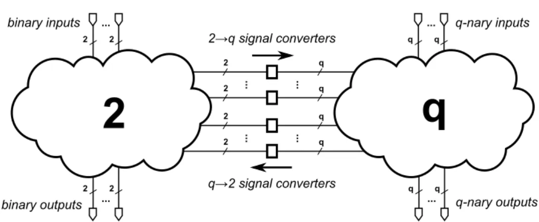
A straightforward solution to mix radices within a single circuit is to use signal conversion, as described in Chapter 3. For example, signal conversion logic can split quaternary signals into pairs of binary signals where appropriate, and vice versa. Conversion can be performed in a rather sophisticated way [71]. The main interest in the conversion approach is the possibility to apply it on top of the existing designs with a minimum computational cost. A major drawback, however, is that the structure of the circuit previously optimised for a certain radix becomes less efficient when converted to a different radix.
The problem can be avoided if mixed radices are applied directly at the logic synthesis stage. The proposal is to develop a mathematical theory for mixing radices in such a way that the radix conversion is done “by construction”. Reed-Muller expansions over Galois fields can be chosen as a foundation for the approach. Since most cryptographic algorithms are based on Galois field arithmetic, we expect these functions to be efficiently mapped into Reed-Muller expansions.
Among a number of MVL synthesis techniques, Reed-Muller expansions over the Galois field of radix 4 are of great interest and have been developed for a number of years. The history of multi-valued Reed-Muller expansions started with evolving functional binary decision diagrams into the theory of Galois switching functions by applying finite field algebra [29, 52]. Later on, this approach has been developed into fixed and mixed polarity quaternary Reed-Muller expansions [28] – acknowledged by MVL research community due to their efficiency and testability. However, the high computational cost has prevented this approach from wide-spread and practical use. Thus, the later research has been focused mostly on optimising the computational algorithms [24, 59, 36, 25] and logic minimisation [34]. An attempt to implement multi-valued Reed-Muller expansions in CMOS has been made as well [81].
Conveniently for the application-driven flow, a Reed-Muller expansion is produced in the form of an arithmetic expression that can be interpreted as a component-level netlist. The expansion itself is a two level function (sum of products), hence the idea to apply different radices to different levels gives the opportunity to develop a variety of two-radix combinations at the higher level of abstraction.
Green’s method [28] has been chosen as an appropriate computation technique. The method is described in Chapter 2. Although it is known for its high computational complexity, it is straightforward and very flexible. At this stage of the research we are interested in the clarity rather than faster runtime. Optimisations can be applied after the entire mixed radix approach is proved valuable.
Given the motivation described in this section, the goal of the research can be defined as follows:
· Implement mixed radix synthesis and conversion approaches as a set of tools. · Interface these new tools to the existing EDA tools, so together they form a
complete design flow for secure devices.
· Explore radix combinations and analyse their efficiency with respect to the circuit parameters and security properties.
1.2
Contribution
Analysis of the existing EDA tools with respect to the security system design has been done prior to the main part of the research. The design flow structure has been proposed for conversion and synthesis approaches. Chapter 3 presents the proposed flows and discusses possible bottlenecks while interfacing between tools. The lack of tool support for encoded MVL synthesis and conversion confirmed the necessity of developing the new tools for these purposes.
Conversion driven design approach has been elaborated and implemented for binary to mixed radix circuit conversion. The basic idea behind the conversion design is
in the grouping of binary gates. Two types of gate grouping have been established: bit-wise and operandbit-wise. Corresponding gate grouping algorithms have been developed and implemented in a tool. The tool supports netlist to netlist conversion; structural Verilog has been chosen as the input and output format.
For synthesis approach, the theory of multi-valued Reed-Muller expansions over Galois field arithmetic has been extended to mixed radix Reed-Muller expansions. The notion of a radix model has been introduced. The developed two-level radix models, presented in Chapter 4, enable computation of the following mixed radix functions:
· radixpufunctions of radixptarguments, wherepis prime andt > u>1; · radixptfunctions of radixparguments, wherepis prime andt >1;
· radixptfunctions of combined radixpand radixptarguments, wherepis prime andt >1;
· radixqfunctions of binary arguments, whereqis any valid Galois field order. The theory of two-level radix models and corresponding computation methods are the primary theoretical contribution of the thesis.
In order to apply the new synthesis theory, the libraries of Galois field arithmetic components have been implemented in compliance with the security requirements and covering the radices 2, 3 and 4. The implementation has been made using runtime library cells and using custom design cells.
Reed-Muller based synthesis has been implemented in RMMixed tool [1]. The tool’s features include:
· computation of uniform radix and mixed radix Reed-Muller expansions in the form of a coefficient vector;
· basic logic minimisation and mapping into component level netlists;
· mapping from the component level to the gate level using provided library of components; the produced output is structural Verilog.
In addition, the tool can assist in calculating miscellaneous expressions in Galois field arithmetic. It can perform basic operations, matrix operations (including inversion), and operations on polynomials (including division). The tool is implemented in two versions: command line tool and TCL console.
The technique has been applied to a real life security related benchmarks in order to provide further motivation for its practical use. Proposed design flow has been tested down to the level of flat technology mapped netlist. Our theory allowed us to compare the efficiency of implemented component libraries in terms of energy consumption, area and delay in a range of radices and radix combinations. We have taken into account that, since the proposed theory is new, it lacks proper optimisation algorithms in comparison with well-developed binary synthesis system. Hence, the benchmark results have been analysed from the perspective of further improvement of the theory.
1.3
Organisation of the thesis
The thesis is organised as follows.Chapter 1 (Introduction) outlines the motivation and application background of the presented research.
Chapter 2 (Background):
· provides technical background for the hardware attacks and countermeasures, outlines the prerequisites for secure design;
· gives the necessary background theory on Galois fields and Reed-Muller expan-sions over Galois fields. The understanding of this theoretical part is essential for reading Chapter 4.
Chapter 3 (Baseline Research) proposes the design flow stucture for conversion and synthesis approaches, gives an overview of the existing tools and outlines the requirements for the new tool. It also presents the conversion driven design
1. Introduction
2.1. Hardware Attacks and Countermeasures
3.1. Secure Design Flow
2.2. Galois Fields and Reed-Muller Expansions
4. Mixed Radix Reed-Muller Expansions
5. Use Case and Experimental Results 6. Conclusions Motivation Background Baseline Main contribution 3.2. Conversion Driven Mixed Radix Design
approach – theoretical part, algorithms and benchmark results – which provides a baseline and further motivation for the main theoretical part of the thesis. Chapter 4 (Mixed Radix Reed-Muller Expansions) presents the theory of mixed
radix Reed-Muller expansions used for logic synthesis in the proposed secure design flow.
Chapter 5 (Use Case and Experimental Results) describes in details the Reed-Muller synthesis-based secure design flow, implemented tool and component libraries and discusses the benchmark results.
Chapter 6 (Conclusion) concludes the work and outlines the possible future develop-ment of the research.
Appendix A (RMMixed User Manual) contains the user manual for Reed-Muller syn-thesis tool.
Some chapters present independent approaches, so there is a certain concurrency in the structure of the thesis. Figure 1.2 illustrates the flow.
Background
The presented research connects two independent aspects: hardware level security and the theory of multi-valued Reed-Muller expansions. This chapter covers the background information for both.
2.1
Hardware Attacks and Countermeasures
As has been discussed in Chapter 1, in order to make the device sufficiently protected against the hardware attacks, certain guidelines must be followed. This section describes the possible dangers and gives the basic understanding of the protection at the hardware level using the special type of signal encoding, known as switching balanced codes.
2.1.1 Types of attacks and countermeasures
Cryptanalysis is mainly divided into software attacks and hardware attacks. Figure 2.1 shows different types of attacks grouped by the field of action [60].
Software cryptanalysis is targetted directly at the cryptographic algorithms, acting at the mathematical level or the level of programming language. This type of attack is not addressed in thie presented research.
Cryptanalysis
Software Hardware
Attacks on cryptography algorithms.
Attacks on software architecture.
Invasive Non-invasive
Reverse engineering. Power analysis. Fault analysis. Timing attacks. Electromagnetic attacks.
Figure 2.1: Types of cryptanalysis
Hardware attacks behave indirectly, using the imperfections of the actual imple-mentations rather than those of the algorithms. These attacks are divided into two major categories: invasive and non-invasive (side-channel). Based on reverse engin-eering, invasive attacks require special laboratory equipment and destroy packaging in the process while side-channel attacks do not require in-depth knowledge of the technology and use simple equipment [60]. With respect to the physical parameter used as the source of information, side-channel attacks are known as power analysis, timing analysis, electromagnetic analysis and fault analysis.
During thepower analysisthe hacker monitors data-dependent power consumption of the device during the normal operation [39]. The method relies on the following fundamental hypothesis: there exists an intermediate variable that appears during the computation of the algorithm, such that knowing a few key bits allows the attacker to decide whether two inputs (respectively two outputs) do or do not give the same value for this variable [18]. Consequently, splitting such variables and combining them with random values can protect against power analysis. This method is calledmasking, and its major advantage with respect to this work is that it can be implemented using standard EDA software. However, recent research has discovered a mathematical modification of power analysis that can break the masking approach [48].
Another countermeasure to the power analysis is to make the device’s power consumption data-independent, it is called power balancing. A number of methods to equalise the power signatures using specific representation of data signals over physical wires, e.g. m-of-n codes, were proposed in [17, 46, 67, 43]. M-of-n codes are an encoding scheme in which data is represented using n wires and where m
of them are set to an active level (usually high). A protocol separating data using dummy symbols (spacers) is called aspacer protocol. In this configuration, the number of wires that switch during the cycle is constant, so is the power consumption. A particular emphasis has so far only been put on dual-rail (1-of-2) codes for binary radix and 1-of-4 for quaternary logic. As a price for the improved resistance to power attacks the approach results in an overhead with respect to the overall power consumption of the system. More details on power balancing using m-of-n codes is given in Subsection 2.1.2.
Electromagnetic analysis is similar to power analysis but uses data-dependent elec-tromagnetic emission instead of power consumption [26]. The method of equalising switching activity of the logic can work in this case as well.
Another way to make the hackers’ life harder is to randomise the timing properties of the circuits, so it would become difficult to perform correct sampling of physical parameters during operation. The simplest method is to insert random delays in the clock cycles. The most reliable countermeasure however is an asynchronous logic design (i.e. self-timed circuits) [46]. Asynchronously working device modules cause overlays in power consumption, thus making it practically impossible to distinguish between single operations. This can help against the timing analysis, which uses the amount of time required for running non constant cryptographic algorithm to retrieve information about the data processed [41].
Fault analysis is an attack which uses abnormal environment conditions, e.g. glitches on power or clock signals, so malfunction of the device can create a window for vulnerabilities [15]. A known countermeasure for this attack is using fault-tolerant protocols. M-of-n codes are fault-tolerant as they imply relatively simple fault detection
logic [14].
Since m-of-n codes and clockless design approach appear to be the most universal countermeasures, the following discussion on the secure design is presented in relation to these ideas.
2.1.2 Power balancing using m-of-n codes
Power balancing is one of the countermeasures to power analysis. It’s concept is to create data-independent power consumption using so-called switching balanced codes and power balanced implementations of logic gates.
CMOS power
Digital circuits consume power whenever they perform computation. Using a constant power supply and input signals to execute, logic cells draw current from the supply and dissipate energy as heat. Power consumption of the circuit is a sum of the power consumption of the individual logic cells.
The overall power dissipation Ptotal of a static CMOS circuit is composed of three components: switching powerPswitch, short-circuit powerPshort and leakage
powerPleak;
Ptotal=Pswitch+Pshort+Pleak.
Short-circuit power Pshort is dissipating due to the presence of a direct path between supply and ground during logical transitions (0 → 1 or 1 → 0). Leakage power dissipationPleak, known as static power consumption, comes from different sources: sub-threshold voltage, tunneling through gate oxide, and through reverse biased diodes. Although at the submicron level the leakage power becomes a relevant factor, short-circuit power and leakage power are considered relatively small compared to the switching power [47].
Switching power Pswitch, also called dynamic power or dynamic dissipation, is attributed to the charging and discharging of capacitances: gate outputs (load
capacit-vdd
A
A
CL Iswitch
Figure 2.2: Switching activity in CMOS inverter
ances) and transistor-to-transistor connections inside gates (intrinsic capacitances) [38];
Pswitch=Pload+Pinternal.
An inverter, shown in Figure 2.2, does not have intrinsic capacitances, hence the load power is equivalent to the dynamic power. During a 0 → 1 transition, current flows from the supply charging the load capacitance CL. Half of the energy is stored in the load capacitor, and the other half is dissipated by the pull-up PMOS network. During a discharging transition 1 →0 current flows from the load to ground, and the energy stored in the load capacitor is dissipated by the pull-down NMOS network; no energy is drawn from the supply. Each switching cycle takes a fixed amount of energy equal toCL·Vdd2 . The inverter’s average dynamic power consumption over some time
period is the integral of the instantaneous power multiplied by switching frequencyf
of 0→1 transitions.
Other CMOS gates and networks of interconnected gates display switching prop-erties other than those of a inverter. Furthermore, they exhibit “lazy switching” characteristics causing a memory effect, where the logical values of outputs are retained from the earlier computation cycles. This memory effect occurs when a gate output computes to the same logical value as the existing output; this naturally happens when more than one set of inputs maps to the same outputs. Similarly, internal nodes exhibit such memory effects and will discharge or charge deterministically. For example, consider the 2-input NAND gate shown in Figure 2.3. It has two parallel
vdd
A
AB
CLB
A
B
CintFigure 2.3: CMOS NAND gate
PMOS transistors and two NMOS transistors connected in series forming the internal transistor-to-transistor capacitance Cint. Assume the inputs are either 00 or 01 and Cint is discharged; if in the next cycle 00 or 01 arrives, then the output will retain its existing value and no power will be consumed. If in the next cycle 10 arrives, the output will retain its value, butCintwill charge, meaning it can freely discharge at any point in subsequent cycles.
Estimating the power consumption of complex gates and networks requires taking into account switching statistics. For instance, from the truth table of the NAND gate the probability of 0 → 1 transition is 3/16, the probability of 1 → 0 transition is also 3/16, and the probability that the output will be retained is 10/16. The concept of switching activity is used to determine the probability of the output switching. ForN
periods of 0→1 and 1→0 transitions, the switching activityαdetermines how many 0→1 transitions occur. Thus,
Pload =αCL·f·Vdd2 ,
where α is the switching activity, CL is output capacitance, and f is the switching
frequency of 0→1 transitions. For the inverter,α=1 andPload=CL·f·Vdd2 .
Pinternal= n X i=1
Figure 2.4: Dual-rail (1-of-2) protocol
estimated using switching activityαi, parasitic capacitanceCiand internal voltageVi
for each nodei. However, in most casesCL is considered to be much bigger than the sum of Ci, so the internal power consumption is often neglected, and the switching power of a particular cell is determined by its load powerPload.
m-of-n codes
Since the main source of power consumption in the CMOS netlist is the switching activity of gates, the method to equalise it is to produce a symmetric switching. This can be achieved using switching balanced codes, for example m-of-n codes.
m-of-n codesare an encoding scheme in which data is represented using n wires and where m of them are set to an active level (usually high).
The simplest example is 1-of-2 code, called dual-rail, which uses a pair of wires per bit of informationd; one wired1 is used for signaling a logic 1 (or true), and another wire d0 is used for signaling logic 0 (or false). Traditionally this code is employed to represent data in self-timed circuits [21]. Viewed together the d1d0 wire pair is a codeword; d1d0 = 10 and d1d0 = 01 represent “valid data” (logic 0 and logic 1 respectively) andd1d0 = 00 represents “no data” (“spacer” or NULL). The codeword
d1d0 =11 is not used, and a transition between valid codewords must be done via the spacer, as illustrated in Figure 2.4.
In asynchronous circuits, dual-rail protocol is used to create a 4-phase handshake protocol, which replaces the clock signal. An abstract view of 4-phase handshaking consist of (1) the sender issues a valid codeword, (2) the receiver absorbs the codeword and sets acknowledge high, (3) the sender responds by issuing the empty codeword, and (4) the receiver acknowledges this by taking acknowledge low [68]. Dual-rail handshake circuit is shown in Figure 2.5.
2n 2n Data, Req
Ack Logic
(dual-rail encoded)
Figure 2.5: 4-phase handshake
Table 2.1: Encoded binary, ternary and quaternary signals.
radix value encoded signal
1-of-2 (dual-rail) 0 01 binary 1 10 NULL 00 1-of-3 0 001 ternary 1 010 2 100 NULL 000 1-of-4 0 0001 1 0010 quaternary 2 or A 0100 3 or B 1000 NULL 0000
An important feature of the dual-rail encoding is its balanced power consumption which facilitates circuit resistance to power analysis attacks. In particular, switching from a spacer to any code word consumes the same amount of power due to the symmetry between rails. The same is true for all m-of-n generalised encodings. Apart from dual-rail we use 1-of-4 to represent quaternary signals and 1-of-3 for ternary. Table 2.1 shows how these encodings can be applied.
single-rail dual-rail x y q=xy x= (x1,x0) y= (y1,y0) q= (q1,q0) 0 0 0 01 01 01 0 1 0 01 10 01 1 0 0 10 01 01 1 1 1 10 10 10 – – – 00 XX 00 – – – XX 00 00
Table 2.2: Dual-rail AND gate truth table and its single-rail equivalence
(a) relaxed balan-cing
(b) fully balanced
Figure 2.6: RTL implementions of dual-rail encoded AND gate showing different levels of power balancing.
Cell implementations for balancing
Since the primary attribute of these codes is balanced switching, the components should also display this feature. Ideally the form and size of the power signature of a component should be symmetrical with respect to switching from spacer to data and vice versa. Usually this is achieved by introducing additional dummy-logic paths. For real life examples an ideal symmetry is impossible, but the components can have certain maximum balancing allowed by the technology capabilities. Such implementations are henceforth calledfully balanced. In contrast, the notion ofrelaxed balancingis used when the security is slightly compromised for significant power and area gains
50 μA -20 μA 50 μA -20 μA 50 μA -20 μA spacer "0", "0" single-rail relaxed fully balanced
spacer "0", "1" spacer "1", "0" spacer "1", "1"
Figure 2.7: Power signatures for different data transitions illustrating the imbalance.
50 μA -20 μA 0 (a) single-rail 50 μA -20 μA 0 (b) relaxed balancing 50 μA -20 μA 0 (c) fully balanced
with so-called “relaxed” balancing, consider a binary AND gate. Table 2.2 shows its truth table. A straightforward dual-rail implementation is shown in Figure 2.6(a). Switching dual-rail inputs[x= (x1,x0),y= (y1,y0)]from the spacer value to["0", "0"],
["1", "0"]and["0", "1"]causes the NOR gate to fire. Switching from the spacer to["1", "1"]
fires the NAND gate. NAND and NOR gates have different switching energy values thus in this case the component is weakly balanced.
In order to improve the balance we have to add logic paths that make the structure of the component symmetrical with respect to the switching activity of the gates and input signals; this is shown in Figure 2.6(b). In the spacer state all inputs are set to low, thus all the outputs of the 2-input NAND gates in the first layer are set to high, precharging the NAND gates in the second layer. Arrival of a data signal (["0", "0"],
["0", "1"],["1", "0"], or["1", "1"]) causes exactly one gate from the first layer to fire. This will produce only one 0 signal to the second layer, switching one of 3-input NANDs. Addition of constant inputs to one of the gates guarantees that all gates in each layer are the same.
Although there are certain unavoidable aspects of the technology, such as transistor level asymmetry which introduces some imbalance even to this design, any implement-ation is acceptable if it fits the requirements of the security standard [5]. For the same reason, the structure shown in Figure 2.6(a) might also be sufficient, since the difference in switching energies is not large. Figure 2.7 displays the analogue simulation results for the components shown in Figure 2.6 along with the non-encoded single-rail im-plementation. As discussed above, fully balanced implementation provides maximum security, while non-encoded circuit is totally unprotected. This is a typical illustration why the standard design flow and tools cannot be directly applied in this area.
A detailed discussion on secure implementations and power balancing can also be found in [31].
2.2
Galois Fields and Reed-Muller Expansions
The section gives a brief yet sufficient background on Galois fields arithmetic, multi-valued Reed-Muller expansions over Galois fields and Green’s direct method of com-putation. The understanding of these theoretical aspects is essential for understanding the theory of mixed radix Reed-Muller expansions. All the theorems in this section are given without proofs. The proofs can be found in the referenced literature. For the extended study of the Galois theory, the reader may refer to [30, 62, 66].
2.2.1 Galois Fields Rings
Definition 2.1. Let Rbe a nonempty set on which we have two closed binary opera-tions, denoted by+and·, i.e.a+b∈Randa·b∈Rfor alla,b∈R. Then(R,+,·)is a
ringif for alla,b,c,∈Rthe following conditions are satisfied [30]: 1. Commutative law of+:a+b=b+a
2. Associative law of+:a+ (b+c) = (a+b) +c
3. There exists azero element[66] (also calledadditive identity[30]), denoted as 0∈R, such thata+0=0+a=afor everyainR.
4. For eacha∈Rthere is an elementb∈Rwitha+b=b+a=0. This element is called theadditive inverseofaand usually denoted as−a.
5. Associative law of·:a·(b·c) = (a·b)·c
6. Distributive law of·over+:
a·(b+c) =a·b+a·c
If, in addition,a·b=b·afor alla,b∈RthenRis called acommutative ring. Aring with unityis a ringRcontaining an element, denoted by 1 and called theunity
or themultiplicative identity, such that for alla∈R
1·a=a·1=a
Definition 2.2. An integral domainis a commutative ring with unity R such that the equationab=0∈Rimplies that eithera=0 orb=0 [66].
Theorem 2.1. A commutative ring with unityRis an integral domain if and only if it satisfies thecancellation law: ifra=rbandr6=0, thena=b[62].
Definition 2.3. Let Rbe a ring with unity. If a ∈ Rand there exists b ∈ R such that
ab= ba=1, thenbis called amultiplicative inverseofa(usually denoted asa−1) and
ais called aunitofR. The elementbis also a unit ofR[30].
Definition 2.4. Commutative ring with unityRis called afieldif every nonzero element ofRis a unit [30].
Znrings
The presented research usesfinite fields, i.e. fields with finite number of elements. The simpliest example isZnrings.
For a fixed positive integer n, define the ring Zn of integers modulo n as
fol-lows [62]. Its elements are the subsets ofZ
[a] = {m∈Z:m≡a(modn)}
= {m∈Z:m=a+knfor somek∈Z}
wherea ∈Z([a]is called the congruence class ofamodn). Addition and multiplica-tion are given by
[a] [b] = [ab]
and[1]is unity. It is routine to check that addition and miltiplication are well defined (that is, if a ≡ a0(modn) and b ≡ b0(modn), then a+b ≡ a0+b0(modn) and
ab ≡ a0b0(modn); i.e, [a] + [b] = [a0] + [b0]and[a] [b] = [a0] [b0]), and thatZn is a
ring under these operations [62].
It is a common practice, when working with Zn, to eliminate brackets from the
notation. InZ3, for example, it is correct to write 2+2=1.
Theorem 2.2. Znis an integral domain if and only ifnis prime [62].
Theorem 2.3. Ifpis a prime, thenZpis a field [62].
Polynomial rings over fields
Definition 2.5. LetRbe a ring. The ringof polynomials in the transcendental (indetermin-ate[30]) variablex, with the coefficients inR,is denoted byR[x]and consists of the set of all formal expressions of the form
f(x) =anxn+an−1xn−1+. . .+a1x+a0
with each ai ∈ R[66]. The elementat ∈ Ris called the coefficient ofxt in f(x) and two polynomials are considered to be equal if and only if, for each t, their nonzero coefficients ofxt are equal. Thezero polynomialhas every coefficient equal to zero and is abbreviated to 0.
The degreeoff(x)is the largestnsuch that the coefficient of xnis nonzero and is denoted by deg(f(x)). Hence deg(0) =0, deg(a0) =0 and deg(ax+b) =1.
If g(x) = bmxm+bm−1xm−1+. . .+b0 we define thesum,f(x) +g(x), to be the polynomial whose coefficient ofxt isat+bt, and we define the product,f(x)g(x), to
be the polynomial whose coefficient ofxtis
Corollary 1. LetR[x]be a polynomial ring.
1. IfRis commutative, thenR[x]is commutative.
2. IfRis a ring with unity, thenR[x]is a ring with unity.
3. R[x]is an integral domain if and only ifRis an integral domain [30].
Irreducible polymonials: finite fields
We now wish to construct finite fields other than those of type(Zp,+,·), wherepis a
prime. The construction will use the following special polynomials.
Definition 2.6. Letf(x)∈F[x], withFa field and deg(f(x))>2. We callf(x)reducible
(overF) if there existsg(x),h(x)∈F[x], wheref(x) =g(x)h(x)and each ofg(x),h(x)
has degree>1. Iff(x)is not reducible it is calledirreducible, orprime[30].
Theorem 2.4. Lets(x)∈F[x],s(x)6=0. Define relationRonF[x]byf(x)Rg(x)iff(x) − g(x) =t(x)s(x), for somet(x) ∈F[x]— that is,s(x)dividesf(x) −g(x)[30]. ThenRis an equivalence relation onF[x].
When the situation described in Theorem 2.4 occurs, we say thatf(x)iscongruent
to g(x) modulos(x) and write f(x) ≡ g(x) (mods(x)). The relationRis referred as
congruence modulos(x).
Z2[x]. Then [0] = x2+x+1=0,x2+x+1,x x2+x+1,(x+1) x2+x+1, . . . = t(x) x2+x+1 |t(x)∈Z2[x] [1] = 1,x2+x,x x2+x+1 +1,(x+1) x2+x+1 +1, . . . = t(x) x2+x+1+1|t(x)∈Z2[x] [x] = x,x2+1,x x2+x+1 +x,(x+1) x2+x+1 +x, . . . = t(x) x2+x+1 +x|t(x)∈Z2[x] [x+1] = x+1,x2,x x2+x+1+ (x+1),(x+1) x2+x+1+ (x+1), . . . = t(x) x2+x+1 + (x+1)|t(x)∈Z2[x]
We now place a ring structure on these equivalence classes [30]. Recalling how this was accomplished in Subsection 2.2.1 for Zn, we define addition by [f(x)] + [g(x)] = [f(x) +g(x)]. Since deg(f(x) +g(x))6max{deg(f(x)), deg(g(x))}, we can always find the equivalence class for[f(x) +g(x)]. Here, for example,[x] + [x+1] = [x+ (x+1)] = [2x+1] = [1]because 2=0 inZ2.
Defining the multiplication of these equivalence classes is a bit more tricky. For instance, what is [x] [x]? If, in general, we define [f(x)] [g(x)] = [f(x)g(x)], it is possible that deg(f(x)g(x)) > deg(s(x)), so we may not readily find[f(x)g(x)] in the list of equivalence classes. However, if deg(f(x)g(x)) > deg(s(x)), then using the division algorithm, we can writef(x)g(x) = q(x)s(x) +r(x), wherer(x) = 0 or deg(r(x))<deg(s(x)). Withf(x)g(x) =q(x)s(x) +r(x)it follows thatf(x)g(x)≡
r(x) (mods(x)), and we define[f(x)g(x)] = [r(x)], where r(x) does occur in the list of equivalence classes.
From these observations we construct tables, shown in Figure 2.9, for the addition and multiplication of{[0],[1],[x],[x+1]}. In these tables we writeafor[a].
Theorem 2.5. Lets(x)be a nonzero polynomial inF[x].
+ 0 1 x x+1 0 0 1 x x+1 1 1 0 x+1 x x x x+1 0 1 x+1 x+1 x 1 0 · 0 1 x x+1 0 0 0 0 0 1 0 1 x x+1 x 0 x x+1 1 x+1 0 x+1 1 x
Figure 2.9: Addition and multiplication of{[0],[1],[x],[x+1]} commutative ring with unity under the closed binary operations
[f(x) +g(x)] = [f(x)] + [g(x)]
[f(x)] [g(x)] = [f(x)g(x)] = [r(x)]
where r(x) is the remainder obtained upon dividing f(x)g(x) bys(x). This ring is denoted byF[x]/(s(x)).
2. Ifs(x)is irreducible inF[x], thenF[x]/(s(x))is a field.
3. If|F|=qanddeg(s(x)) =n, thenF[x]/(s(x))containsqnelements [30].
Definition 2.7. Let (R,+,·) be a ring. If there is a least positive integer n such that
nr = r+. . .+r(ntimes) = 0 ∈ Rfor allr ∈ R, then we say thatRhascharacteristicn
and write char(R) =n. When no such integer exists,Rsaid to have characteristic 0. Theorem 2.6. Let(F,+,·)be a field. Ifchar(F)>0, thenchar(F)must be prime.
Theorem 2.7. A finite fieldFhas orderpt, wherepis a prime andt∈Z+.
Theorem 2.8. (Galois) For every primepand every positive integert, there exists a field having exactlypt elements [62].
Corollary 2. (E.H. Moore) Any two finite fields of orderptare isomorphic [62].
These fields were discovered by the French mathematician Evariste Galois (1811– 1832) in his work on the nonexistence of formulas for solving general polynomial equations of degree > 5 over Q. As a result, a finite field of order pt is denoted by GF pt, where the letters GF stand forGalois field.
Definition 2.8. IfEis a field andFis a subset which, under the operations ofE, is itself a field thenFis called asubfieldofEandEis anextensionofF[66]. GF(p) is a subfield of GF(pt) for any primepandt >1.
Definition 2.9. Ahomomorphismψ:F→F0of fieldsis a ring map
(ψ(a+b) =ψ(a) +ψ(b),ψ(ab) =ψ(a)ψ(b))
such thatψ(1) =1. Ifψis one-to-one and onto, it is anisomorphism(anautomorphismif
F=F0). [66].
If the fieldsFandF0 are homomorphic only with respect to one of the operations, i.e. eitherψ(a+b) = ψ(a) +ψ(b)or ψ(ab) = ψ(a)ψ(b) is true forψ :F → F0, the fieldFis called asubgroupofF0under the operation of addition (multiplication).
The next subsection summarises the properties of Galois fields used in the defini-tion and the computadefini-tion of Reed-Muller expansions.
Galois field properties overview
For anyq = pt, wherepis a prime number and integert >1, a Galois field GF(q) is defined as an algebraic structure consisting of:
1. qelements;
2. closed binary operations+and·called addition and multiplication respectively, i.e.a+b∈GF(q)anda·b∈GF(q)for alla,b∈GF(q);
3. elements 0 and 1 such thata+0=aanda·1=afor allx∈GF(q).
4. Operations of addition and multiplication have the property of commutativity, transitivity, and the operation of multiplication is distributive over addition. For everya ∈ GF(q), there exists−a ∈ GF(q)such thata+ (−a) = 0 [52]. Similarly, for every nonzerob∈GF(q), there existsb−1∈GF(q)such thatb·b−1=1.
GF(2): + 0 1 0 0 1 1 1 0 × 0 1 0 0 0 1 0 1 GF(3): + 0 1 2 0 0 1 2 1 1 2 0 2 2 0 1 × 0 1 2 0 0 0 0 1 0 1 2 2 0 2 1 GF(4): + 0 1 A B 0 0 1 A B 1 1 0 B A A A B 0 1 B B A 1 0 × 0 1 A B 0 0 0 0 0 1 0 1 A B A 0 A B 1 B 0 B 1 A
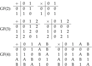
Figure 2.10: Addition and multiplication over some finite fields
Another important property of the Galois fields is that for everya∈GF(q),aq=a
and fora 6= 0, aq−1 = 1 [52]. Hence the number of possible powers ofain GF(q) is limited toq.
The elements of prime Galois fields are denoted as integer numbers. In the case of GF(pt), firstpelements are denoted as integers, as they are the elements of the prime subfield GF(p), and the rest of the elements assign consequent uppercase latin letters:
A,B, . . .. For example the elements of GF(4) are: 0, 1,A,B.
Arithmetic operations for some Galois fields used in the further examples are shown in Figure 2.10.
Matrix operations over Galois fields
The presented research extensively uses matrix operations over Galois fields. Due to the properties of Galois fields, the matrix operations are defined in the same way as in regular algebra. The elements of matrices are the elements of some field GF(q).
Matrix addition is defined as
[X+Y]i,j =Xi,j+Yi,j,
IfXis anm-by-nmatrix andY isn-by-pmatrix, then theirmatrix productXYis the
m-by-pmatrix whose entries are given by dot-product of the corresponding row ofX
and the corresponding column ofY:
[XY]i,j = n X r=1
Xi,rYr,j,
where 1 6 i 6 m and 1 6 j 6 p. Matrix multiplication satisfies the rules(XY)Z = X(YZ)(associativity), and(X+Y)Z=XZ+YZas well asZ(X+Y) =ZX+ZY(left and right distributivity), whenever the size of the matricesX,Y,Zis such that the various products are defined.
In linear algebra an n-by-n (square) matrixXis calledinvertible, if there exists an
n-by-nmatrixYsuch that
XY=YX=In
whereIn denotes then-by-n identity matrix and the multiplication used is ordinary
matrix multiplication. If this is the case, then the matrixYis uniquely determined byX
and is called theinverseofX, denoted byX−1. Non-square matrices (m-by-nmatrices
for whichm6=n) do not have an inverse.
Definition 2.10. IfXis anm-by-nmatrix andYis ap-by-qmatrix, then the Kronecker product[23] is themp-by-nqblock matrix
X⊗Y = x1,1Y · · · x1,nY .. . . .. ... xm,1Y · · · xm,nY
Kronecker product is not commutative, but it is associative: (X⊗Y)⊗Z = X⊗
(Y⊗Z) for matrices X,Y,Z. One of the properties of Kronecker product used in the presented theory is that for any invertible matricesXandY, (X⊗Y)−1 = X−1⊗Y−1;
2.2.2 Multi-valued Reed-Muller expansions
Binary and multi-valued functions can be represented using XOR sum of products. One particular case is Muller (RM) expansions. In the multi-valued case, Reed-Muller expansions have the form of sum of products computed over GF(q).
The following simplified definition of literal is used in this thesis; it is sufficient for understanding the theory at the required level. For classic definition of literal and literal form of Reed-Muller expansions, refer to [35, 34].
Definition 2.11. Literalexof theq-valued variablexis one ofqpossible polarity forms (x+c);cis an element of GF(q) denoting the literal.
Definition 2.12. For ann-variableq-valued functionpolarity numberkis defined as an integer representation of aq-nary tuplehkn. . .k1iq=kwhereki∈GF(q)denotes the
polarity of literalexi,i = 1 . . .n. For example, the polarity numberk = 2 = h0Ai4 for
2-variable quaternary function means thatex2 =x2andex1 =x1+A.
Definition 2.13. A general canonical Reed-Muller (RM) expansion for an n-variable q -valued function in polaritykis defined as follows:
f(ex1, . . . ,exn) = qXn−1 i=0 ai n Y j=1 e xij j over GF(q) (2.1)
where ij is a single digit of a q-nary tuple hin. . .i1iq = i. Vector a =
a0 . . . aqn−1
t
is acoefficient vector. In afixed polarityRM expansion each variable must be represented by the same literal throughout the expansion.
Following from Definition 2.10 of the Kronecker product, (2.1) can be rewritten in matrix form. LetXej =
1 exj . . . ex
q−1
j
is the vector of all possible powers of the literalexj, then f(ex1, . . . ,exn) = e Xn⊗. . .⊗Xe1 ·a over GF(q) (2.2) where a is a coefficient vector as in Definition 2.13. Equation (2.2), as well as (2.1), represents the sum of all possible products of all possible powers of the input variables
multiplied by coefficients froma.
Reed-Muller expansion of zero polarity for a quaternary function of one variable takes the form:
f(x) =a0+a1x+a2x2+a3x3 over GF(4) (2.3) As an example, a 2-variable quaternary function of the polarityk=2=h0Ai4gives the following RM form:
f(x1,x2) = a0+a1x¨1+a2x¨21+a3x¨31+
a4x2+a5x¨1x2+a6x¨21x2+a7x¨31x2+ a8x22+a9x¨1x22+a10x¨21x22+a11x¨31x22+ a12x32+a13x¨1x32+a14x¨21x32+a15x¨31x32
computed over GF(4); ¨x1=x1+A.
2.2.3 Green’s direct method
The computation of an RM expansion corresponds directly to the computation of the coefficient vectora. The following method of computation has been proposed in [28] for quaternary RM expansions and is known asGreen’s direct method.
Letd =
d0 . . . d3 t
, d0. . .d3 ∈GF(4)be the truth vector of the zero polarity quaternary functionf(x)shown in (2.3). Then,
d0 = f(0) = a0
d1 = f(1) = a0+a1+a2+a3 d2 = f(A) = a0+Aa1+Ba2+a3
d3 = f(B) = a0+Ba1+Aa2+a3
This set of linear equations can be solved in matrix form: d= 1 0 0 0 1 1 1 1 1 A B 1 1 B A 1 ·a=S0a over GF(4) (2.5) a=S−01d=W0d over GF(4) (2.6) W0= 1 0 0 0 0 1 B A 0 1 A B 1 1 1 1
Hence a coefficient vector a can be derived from the truth vector of a function. For non-zero polarity forms (k = 1 . . . 3) of a 1-variable quaternary function the same approach can be applied, and corresponding matricesW1,W2,W3can be found:
S1 = 1 1 1 1 1 0 0 0 1 B A 1 1 A B 1 , W1=S−11 = 0 1 0 0 1 0 A B 1 0 B A 1 1 1 1 ; S2 = 1 A B 1 1 B A 1 1 0 0 0 1 1 1 1 , W2=S−21 = 0 0 1 0 B A 0 1 A B 0 1 1 1 1 1 ; S3 = 1 B A 1 1 A B 1 1 1 1 1 1 0 0 0 , W3=S−31 = 0 0 0 1 A B 1 0 B A 1 0 1 1 1 1 .
Generally, for any n-variable quaternary function defined by its truth vector d, a coefficient vector a of k-polarity RM expansion can be found from the following equation:
d= (Skn⊗. . .⊗Sk1)·a over GF(4)
derived from (2.2), wherehki10 =hkn. . .k1i4as in Definition 2.12. Using the properties
of the Kronecker product, this equation can be solved as follows:
a= (Skn⊗. . .⊗Sk1)−1·d over GF(4) (2.7) (Skn⊗. . .⊗Sk1)−1 = S−k1 n⊗. . .⊗S −1 k1 = Wkn⊗. . .⊗Wk1
According to Definition 2.12,n-variableq-nary function can haveqnfixed polarity forms. During the synthesis process RM expansions are computed for all polarity forms in order to find the optimal solution. More computationally efficient algorithms than the direct method exist [59, 36, 25]. They exploit certain properties of GF(4) while Green’s method is based on a general principle that can be extended to other radices. Denoting the truth vector of a one-variable q-nary function f(x) as d =
d0 . . . dq−1
t
, d0. . .dq−1 ∈ GF(q), one can create a matrix equation similarly to the steps (2.4)—(2.6):
a=S−k1d
where the polarity number k = 0 . . .q−1. As far as the matrices S0. . .Sq−1 are
invertible in GF(q), corresponding matricesW0. . .Wq−1 can be found and then used
to computen-variable RM expansions of radixqusing (2.7).
Binary RM expansion of one-variable function takes the form:
f(ex) =a0+a1ex over GF(2)
Let the truth vector be defined asd=
d0 d1
. For zero polarity caseex=x, hence:
d0 = f(0) = a0 d1 = f(1) = a0+a1 a= 1 0 1 1 −1 ·d= 1 0 1 1 ·d over GF(2) (2.8)
For polarity 1 we haveex=x+1, so the set of equations is changed correspondingly: d0 = f(0+1) = f(1) = a0+a1 d1 = f(1+1) = f(0) = a0 a= 1 1 1 0 −1 ·d= 0 1 1 1 ·d over GF(2) (2.9)
From (2.8) and (2.9) we have:
W0 = 1 0 1 1 W1= 0 1 1 1
The following example illustrates how Green’s method can be used to obtain a binary circuit from a set of truth vectors.
vectorsd0andd1respectively.
d0 = [11001110]t d1 = [11111101]t
Binary case matrices W0 and W1 shown above can be used to compute the RM expansions. For polarityk = 0 = h000i2, the coefficient vector forF0 can be found as follows: a = (W0⊗W0⊗W0)·d0 over GF(2), a = 1 0 1 1 ⊗ 1 0 1 1 ⊗ 1 0 1 1 ·d0 = 1 0 0 0 0 0 0 0 1 1 0 0 0 0 0 0 1 0 1 0 0 0 0 0 1 1 1 1 0 0 0 0 1 0 0 0 1 0 0 0 1 1 0 0 1 1 0 0 1 0 1 0 1 0 1 0 1 1 1 1 1 1 1 1 · 1 1 0 0 1 1 1 0 = 1 0 1 0 0 0 1 1 .
ComputingF1for the polarity numberk=1=h001i2:
a = (W0⊗W0⊗W1)·d1= [10000001]t
The functions can be expressed using the computed coefficient vectors as follows.
F0(y0,y1,y2) = 1+y1+y1y2+y0y1y2 F1(y0,y1,y2) = 1+y0y1y2
Figure 2.11: Binary RM expansion, component-level schematic.
clearly observed “layers”: a layer of sums (marked asΣ), a layer of products (Π) and a layer of polarities (ex). The number of components has been also optimised by reusing
the results of some operations. For example, the termy1y2is reused three times. Example 2.2. Let two-variable quaternary function be defined by the truth vectord = [BBAABB1ABBAABB1A]t.
Quaternary RM expansion gives