Technology (IJRASET)
Implementation of 8-bit Sigma-Delta ADC using
45nm Technology
Yogita Tembhre#1, Anil Kumar Sahu*2
#
ETC, SSTC, SSGI (FET) Bhilai, India
Abstract— Design for oversampling sigma-delta (ΣΔ) ADCs is conferred here. In this paper a contemporary design for 8-bit ΣΔ oversampling ADC is presented, in which first order oversampling ΣΔ modulator and the decimation filter is second order
Cascaded Integrated Comb (CIC) filter which is utilized. Transistor level circuit design and output simulation of the sigma-delta ADC with a power supply of 1V is presented here. This architecture is implemented by Tanner EDA tool v15.0 using 45nm BSIM4 CMOS technology.
Keywords— 8-bit Sigma-Delta ADC, BSIM4, CIC filter, Oversampling, Sigma delta modulator.
I. INTRODUCTION
Oversampling ΣΔ ADCs are pervasively termed as oversampling ADCs. ΣΔ ADCs become popular in nano-CMOS technologies as
the higher sampling rates allow higher transference bandwidths while reaching medium resolution. Initially ΣΔ ADCs was applied
on audio and other sensing applications which require high-resolution, but recently, these modulators are widely utilized in reconfigurable radio and wireless communication systems. A ΣΔ ADC based on two aspects noise shaping and oversampling, which
allow higher data conversion accuracy, i.e. optimum trade off between resolution and speed. Also, oversampling diminishes the necessity of the anti-aliasing filter with the modulator [1]. ΣΔ -Modulators are trending in ADCs because of the high accuracy results in standard low-cost CMOS technology. Being an oversampling converter, ΣΔ -ADCs do not have a direct input to output relationship.
Oversampling ADCs may be designed by using either discrete-time (switched-capacitor) loop-filter or a continuous-time loop filter. Both the style has some benefits as well as drawbacks. The discrete-time ΣΔ ADCs is used in industrial designs, whereas the
continuous-time ΣΔ ADCs is popular with the academics. CT-ΣΔ ADCs are becoming popular in broadband wireless
communication systems because of some desirable features which include anti-aliasing filtering, with relaxed bandwidth requirements of the active elements and lower power consumption. However, there are few challenges in the adoption of CT-ΣΔ
ADCs in industries due to the complex design because of a hybrid CT and DT system, and sensitiveness to the TRC (time constant)
of RC circuit and also timing jitter [10].
II. PREVIOUSWORK
With the improvements of IC technologies it is difficult to obtain a low power supply and devices with shorter channel length. Preferably, opamps with a large dc gain were avoided by single stage modulator circuits. Despite, practically it is tough to make
stable higher order single stage modulators. The first order ΣΔ modulator has many benefits over other higher order ΣΔ modulators
as on area, performance, and power consumption [6]. DT ΣΔ modulator importantly shortens the necessity of interference and the
operational amplifier gain by using noise shaping technology, well capacitive matching features and oversampling, so it is very
pertinent for lower voltage applications [9]. Alternatively ΣΔ modulator can also be designed based on LDI ladder (lossless digital integrator) for high order and stable oversampled oscillator using modulation techniques [5].
III. PROPOSEDCIRCUIT
A. First Order Sigma Delta Modulator
Technology (IJRASET)
[image:3.612.148.463.105.198.2]as a feedback. The main task of the modulator is to encode an analog signal to 1-bit digital bit stream which equal to the actual value.
Fig. 1. Basic first order modulator Architecture
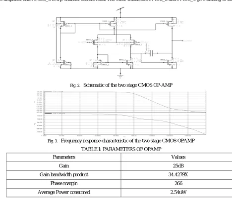
[image:3.612.62.530.304.711.2]1) OP-AMP: The diagram below depicts the two-stage CMOS op-amp transistor level circuit design. The first phase is used as differential input while the second stage is used for additional voltage gain. The first stage of the op-amp considered comprises transistor (PMOS_1, PMOS_2, NMOS_1, NMOS_2, and PMOS_4). Here transistors PMOS_1- PMOS_2 and NMOS_1- NMOS_2 are p-channel differential transistor pair and n-channel current sourcing mirror load respectively, and transistor PMOS_4 is a tail current source transistor. The second phase contains the transistors PMOS_5, NMOS_3 in which PMOS_5 is n-channel common-source amplifier and NMOS_3 is a p-channel current load. The other transistors PMOS_3 and PMOS_6 give biasing to the circuit.
Fig. 2. Schematic of the two stage CMOS OP-AMP
Fig. 3. Frequency response characteristic of the two stage CMOS OPAMP
TABLE I: PARAMETERS OF OPAMP
Parameters Values
Gain 25dB
Gain bandwidth product 34.4279X
Phase margin 266
Technology (IJRASET)
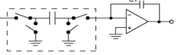
2) Switched-Capacitor Integrator: Switched-capacitor integrator is used to design the modulator. A switched-capacitor integrator consists of two capacitors, (a sampling capacitor and a hold capacitor), an op-amp and switches (S1, S2, S3 and S4). The clock
signals Φ1 and Φ2 applied to form non-coinciding clock signals. Switches S1 and S3 are ON and switch S2 and S4 initially OFF
when clock Φ1 is high and start to charge the sampling capacitor, Cs until equal the input voltage. When clock Φ1 fall, clockΦ2
start to rise and at the same time S1 and S3 are OFF while switches S2 and S4 turn ON which connecting the sampling capacitor, Cs [11].
Fig. 4. Circuit diagram of Switched-capacitor Integrator
[image:4.612.219.396.167.223.2]3) COMPARATOR: To design the comparator, we just used the two-stage op-amp makes some modification on it so that it acts like a comparator. The modification that needs to do is just removed the compensation capacitor 0.5pF from the actual circuit of the two-stage op-amp.
Fig. 5. Schematic of Comparator
Fig. 6. Waveform of Comparator
After complete designing all the components-part that required in the modulator, all the components-parts are combining all
together to make a complete design of the ΣΔ modulator. The non-overlapping input for the switched-capacitor integrator is from
[image:4.612.196.433.302.473.2]Technology (IJRASET)
Fig. 7. Input and output waveform of ΣΔ modulator
B. Decimation Filter
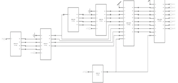
The architecture of decimation filter that being used is the Cascaded Integrated Comb (CIC) filter. There are two essential building blocks integrator and differentiator in the first order CIC filter. The integrator considered is an IIR filter having single pole with identity response coefficient, which also acts as the accumulator. The single integrator is unstable due to the single pole at z = 1, due to this there is a high chance of register overflow and data may be lost. To avoid this problem, two's complement technique is considered [7]. Since here CIC filter is used, the order of CIC filter is can be determined by looking the sigma-delta modulator used. For the given condition, here first order sigma-delta modulator is used, i.e. L = 1, hence the CIC filter is used in the order of k = L + 1. It is clear that to properly undermine the quantization noise a second order CIC filter is required. Since we deal with high order and sampling rates, the circuit becomes more complex. To minimize the complicatedness a decimation stage is introduced between integrator and differentiator stage. The clock divider divides the oversampling frequency by the oversampling ratio (K) before going into the differentiator while the integrator operates in the oversampling frequency. Since the differentiator operates in low frequency it makes a reduction in power consumption. There are two major stages which are integrator stage and differentiator stage. The implementation of the concept of second order CIC filter in circuit design is as shown in Figure as we want to produce an 8-bit digital response.
Fig. 8. Circuit diagram of decimation filter
C. Level Shifter
[image:5.612.160.463.391.533.2]Technology (IJRASET)
Fig. 9. Input and Output waveform of level shifter
IV. SIMULATIONANDRESULTOFSIGMADELTAADC
The ΣΔ ADC is created using a Tanner EDA tool v15.0 using a 45nm BSIM4 CMOS process, the supply voltage is 1V. All the main
parameters of the described 8-bit ΣΔ ADC are summed up in the Table II given below. Oversampling ΣΔ ADC is designed by using ΣΔ modulator, level shifter and decimation filter. Fig. 14 depicts the 8-bit oversampling ΣΔ ADC.
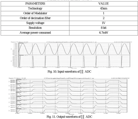
TABLE II: PARAMETERS OF ADC
PARAMETERS VALUE
Technology 45nm
Order of Modulator 1
Order of decimation filter 2
Supply voltage 1V
Resolution 8 bit
Average power consumed 6.7mW
[image:6.612.72.538.304.705.2]Fig. 10. Input waveform of ΣΔ ADC
Technology (IJRASET)
TABLE III
COMPARISON OF PRESENT WORK WITH PREVIOUS WORK
TECHNOLOGY (CMOS) SUPPLY VOLTAG E RESOL -UTION ORDER OF MODUL-ATOR POWER CONSUMPTIO N REFERENCE S
0.35um double-poly treble
metal 5/3 16 2 300mW [1]
0.18um one-poly six metal 1.8 12 0-3MASH 24mW [2]
0.35um 3.3 10 1 12.2mW [4]
0.18um double poly five
metal 1.8 14 5 150mW [6]
0.045um BSIM4 1 8 1 6.7mW Present work
V. CONCLUSION
This paper has presented a technique of designing first order sigma delta ADC. A design procedure for first order ΣΔ modulator and second stage CIC filter for decimation filter was presented. This ΣΔ ADC is can be further used in the ADC BIST pattern to detect the faults present in any given problem. The present paper gives the ΣΔ ADC in Tanner EDA tool v15.0 using 45nm BSIM4 CMOS
technology. The advantages of first stage modulator over other modulators are on performance, power dissipation and also stability.
VI. ACKNOWLEDGMENT
The authors would like to thank the management, SSTC SSGI institute for providing Tanner EDA Tool v15.0.
REFERENCES
[1] Li Liang, Ruzhang Li, Zhou Yu, Jiabin Zhang and Jun'an Zhang, "A 16-bit cascaded sigma-delta pipeline A/D converter" Journal of Semiconductors , May 2009, pp. 550101-550106.
[2] A. Gharbiya and David A. Johns, "A 12-bit 3.125 MHz bandwidth 0-3 MASH delta-sigma modulator" IEEE Journal of Solid-State Circuits, July 2009, pp. 2010-2018.
[3] L. Liu, Li Dongmei, Chen Liangdong, Ye Yafei and Z. Wang, "A 1-V 15-bit audio-ADC in 0.18 m CMOS" IEEE Transactions on Circuits and Systems, May 2012, pp. 915-925.
[4] L. Hernández Corporales, Prefasi Enrique, Pun Ernesto and Patón Susana "A 1.2-MHz 10-bit Continuous-Time Sigma-Delta ADC Using a Time Encoding Quantizer" IEEE Transactions on Circuits and Systems, January 2009, pp. 16-20.
[5] Dallet Dominique, Chiheb Rebai, and Marchegay Philippe "Signal generation using single-bit sigma-delta techniques" IEEE Transactions on Instrumentation and Measurement, August 2004, pp. 1240-1244.
[6] R. Jiang, and S. Fiez Terri "A 14-bit delta-sigma ADC with 8× OSR and 4-MHz conversion bandwidth in a 0.18-μm CMOS process" IEEE Journal of Solid -State Circuits, January 2004, pp. 63-74.
[7] M. Arifuddin Sohel, K. Chenna Kesava Reddy and Syed Abdul Sattar. "Design of low power Sigma Delta ADC" International Journal of VLSI design & Communication Systems, August 2012, pp. 67-80.
[8] Yamei Li and He. Lili "First-order continuous-time sigma-delta modulator" IEEE International symposium on Quality Electronic Design, March 2007, pp. 229-232..
[9] R. Laajimi, "First order sigma-delta modulator with low-power consumption implemented in ams 0.35 µm cmos technology" International Journal of Research in Engineering and Technology, April 2013, pp. 700-705.
[10] V. Acharya, "MWSCAS 2012 Tutorial Proposal Delta-Sigma Analog-to-Digital Converters-From System Architecture to Transistor-level Design".
[11] Nowshad Amin, Goh Chit Guan, and Ahmad Ibrahim, "An efficient first order sigma delta modulator design." IEEE In Electrical and Computer Engineering, 2008, pp. 000029-000032..