5
XI
November 2017
Surface Stability studies of Porous Silicon with
Si-Ag Bonds
Gunjan Aggarwal1, S. S. Islam2 1
D/o Electronics and Communication, IIMT College of Engineering, Greater Noida, India. 2
Centre of Nanoscience and Nanotechnology, Jamia MilliaIslamia (A Central University), New Delhi, India.
Abstract: In this paper, the authors have reported the improved surface stability studies of porous silicon by depositing metal (Ag) nanoparticles followed by electrochemical anodization of silicon to make it porous. The root cause for surface degradation
of porous silicon is passivation of Si-Hxbonds with oxygen termination and its replacement by Si-Ag bonds seems to have
eradicated the degradation factor to a great extent. The surface quality has been checked periodically and any noticeable degradation is not observed in PS sample with Si-Ag bonds for one year. The qualitative analysis of the surface morphology (microstructure) was analyzed by scanning electron microscope (SEM) fitted with Energy-dispersive X-ray spectrometer (EDX).Micro-Raman, Photoluminescence (PL) and Fourier Transform Infrared (FTIR) spectroscopy were use o study surface bond termination and degradation, if any.
Keywords: Porous Silicon; Surface Stability; Si-Ag Bonds; scanning electron microscope (SEM); Micro-Raman; Fourier Transform Infrared (FTIR) spectroscopy.
I. INTRODUCTION
Since the discovery of visible luminescence from porous silicon by L.T. Canham [1], a strong interest and hype was generated among the researchers for its enormous potential applications in the field of microelectronics [5], sensors [6] [7] [8], biochemistry [9][10] and optoelectronics [11] [12].
Somehow the interest on porous silicon has been waned away mainly because of its surface instability as no long term device can be made where surface deradation changes the device characteristics with time. The degradation even starts immediately after the exposure to ambient air. This compelled the researchers to look into this fundamental problem with a view to arrest the cause by evolving new concept and technology.
Numerous treatments to stabilize porous silicon structure have been reported like chemical treatment [13][14], carbonization [15], thermal treatment [16] [17] and photo-induced electrochemical anodization method [18], but till date no method have shown any long term surface stability of porous silicon.
In this report, authors have carried out the two step method viz chemical followed by electrochemical method on the PS samples to prepare Si-Ag bonds on the PS surface. The sample was then investigated through scanning electron microscope (SEM), micro-Raman, Photoluminescence (PL), Energy-dispersive X-ray spectroscopy (EDX) and Fourier Transform Infrared (FTIR) spectroscopy. The results show no surface degradation even after one year.
II. EXPERIMENTAL
III. RESULTS AND DISCUSSION
A. SEM Analysis
For surface structural analysis, Field Emission Scanning Electron Microscope (FEI, Nova Nano SEM 450) was used. The SEM image (Fig.1a) of as-prepared porous silicon sample indicates the presence of well-dispersed nanopore distribution of diameter in the range 40-60 nm.
[image:3.612.54.548.58.296.2]Fig.1b)shows the SEM images of the sample after Si-Ag bonds formation. It is observed that silicon have a layer of silver (Ag) on the top of its surface. These results were verified by Energy-dispersive X-ray spectroscopy (EDS). The EDS spectra (Fig. 2) of the sample surface indicate the silver content. The table inserted in the fig. 2 shows that total Ag content on the surface of sample was around 67.65% while silicon content was around 33%. It is seen that a measurable quantity of Ag deposited on the surface of the silicon.
Fig 1.SEM image of Sample a) As-etched, b) and c) After Si-Ag formation. Silicon sample was treated with an aq. solution of HF and AgNO3 at T=50 °C
and time of 60 min.
Sample was put in dilute nitric acid for four days to remove its excess silver coating.
Sample was rinsed with DI water followed by electrochemical anodization.
The etchant solution is consisted of HF, C2H5OH and H2O (1:1.5:2); and the
current density was 30 and 20 mA/cm2for the first 30 and second 30 min,
respectively
.
El AN Seriesunn. C norm. C Atom.
[wt.%] [wt.%] [at.%] ---
Ag 47 L-series 67.65 66.94 34.52 Si 14 K-series 33.40 33.06 65.48 --- Total: 101.05 100.00 100.00
c) b)
[image:3.612.78.539.421.569.2]Fig 2.EDS spectra of Sample after the formation of Si-Ag bonds.
B. RAMAN Analysis
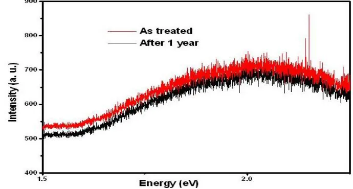
Fig. 3 shows the Raman spectra of as-treated sample and after one year of the same sample. The peak of PS shifts at 519cm-1 in Raman profile. Raman spectra of PS confirm (a) faster etching rate, (b) in porosity of porous silicon (PS), and (c) decrease in silicon crystallite size [2]. Raman results also show that the smaller the mean crystallite size, the greater is the redshift and asymmetry in the lower energy of the LO phonon mode.
Fig 3.Raman spectra of PS Sample of as-treated and after one year.
C. Photoluminescence (PL) Analysis
[image:4.612.128.483.326.443.2]PL analysis was done to check the surface stability of PS sample over a period of one year (Fig. 4). With aging the surface of porous silicon samples degrades while creating surface functional complex either with oxygen, or hydrogen or both. Due to treatment, blue shifted PL peak was observed at 1.97eV. After one year of shelf life, it was observed that PL of sample shows almost overlapping spectra, which shows good stability of PS surface.
Fig 4.PL spectra of PS Sample of as-treated and after one year.
2 4 6 8 10 12 14
keV 0
1 2 3 4
5 cps/eV
Ag
Ag Si
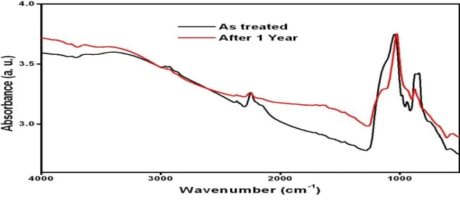
[image:4.612.132.477.538.723.2]C. FTIR Analysis
[image:5.612.141.472.158.302.2]FTIR studies have been performed in the range of 500 to 4000 cm-1 for the identification of the functional group attached on the surface of samples of as-treated and after one year. For both samples the observed peaks at 2250 and 857 cm-1 are attributed Si-H stretching and deformation vibration modes [19] [20]. The absorption peak at 1033 cm-1 is attributed to Si-O-Si bond [21]. The surface treated sample was periodically checked for one year and it was found that all specific modes mentioned above retain their characteristic peak position and intensity and this confirms the achievement of surface stability.
Fig 5.FTIR spectra of PS Sample of as-treated and after one year.
IV. CONCLUSION
Silver atoms of the sample can easily terminate the surface dangling bonds which can replace the less stable Si–H bonds resulting in the formation of more stable Si–Ag bonds. Silver is expected to be spread on the surface of PS and hence prevent the sample against passivation by oxygen in ambient atmosphere. The chemical properties of Ag are similar to those of Au(gold), therefore, expected to form Si–Ag bonds on the PS surface. Like Au deposition on silicon surface, Si–Ag bonds were also found to remain stablefor one year time span. Further studies are in progress to check its time dependent evolution of the quality of the surface.
V. ACKNOWLEDGEMENTS
The authors gratefully acknowledge the financial support provided by Department of Science &Technology, Govt. of India, through its Grant No.SR/S2/CMP-0053/2009 to carry out this work.
REFERENCES
[1] Canham, L. T., (1990), Silicon quantum wire array fabrication by electrochemical and chemical dissolution of wafers, Appl. Phys. Lett., Vol. 57,1046-1048. [2] Bisi,O.,Ossicini, S. and Pavesi, L., (2000), Porous silicon: a quantum sponge structure for silicon based optoelectronics, Surf. Sci. Rep., Vol. 38, 1-126. [3] Kordas, K.,Beke, S., Pap, A. E.,Uusimaki, A., and Leppavuori, S., (2004), Optical properties of porous silicon.Part II: Fabrication and investigation of
multilayer structures, Opt. Mater. (Amsterdam, Neth.), Vol. 25, 257-260.
[4] Lammel, G., Schweizer, S., and Renaud, P., (2001), Microspectrometer based on a tunable optical filter of porous silicon, Sens. Actuators A, Vol. 92, 52-57. [5] Benson, T. M., Arrand, H.F., Sewell, P., Niemeyer, D., Loni, A.,Bozeat, R. J., Kruger, M.,Arens-Fischer, R., Thonissen, M., and Luth, H.,(1999), Progress
towards achieving integrated circuit functionality using porous silicon optoelectronic components, Mater. Sci. Eng. B, Vol. 69-70, 92-99.
[6] Holec, T.,Chvojka, T., Jelínek, I.,Jindrich, J.,Nemec, I.,Pelant, I., Valenta, J., and Dian, J., (2002), Determination of sensoric parameters of porous silicon in sensing of organic vapors, Mater. Sci. Eng. C, Vol. 19, 251-254.
[7] Foucaran, A., Pascal-Dellamnoy, F., Giani, A., Sackda, A., Combette, P., and Boyer, A., (!997), Porous silicon layers used for gas sensor applications, Thin Solid Films, Vol. 297, 317-320.
[8] Dhanekar, S., Islam, S. S., Islam, T., Harsh, (2010),Highly Sensitive Porous Silicon Sensor: Detection Of Organic Vapours using PhotoluminescenceQuenching Technique, Int. Jrnl. on Smart Sensing and Intelligent Systems, Vol. 3, 1-13
[9] Zairi, S.,Martelet, C.,Jaffrezic-Renault, N., M’Gaieth, R., Maaref, H., and Lamartine, R., (2001), Porous silicon a transducer material for a high-sensitive (bio)chemical sensor: effect of a porosity, pores morphologies and a large surface area on a sensitivity, Thin Solid Films, Vol. 383, 325-327
[10] Luth, H., Thust, M., Steffen, A., Kordos, P., and Schoning, M. J., (2010), Biochemical sensors with structured and porous silicon capacitors, Mater. Sci. Eng. B, Vol. 104, 69-70
[11] Martin-Palma, R. J., Martinez-Duart, J. M., Li L., and Levy, R. A., (2002), Electrical behavior of double-sided metal/porous silicon structures for optoelectronic devices, Mater. Sci. Eng. C, Vol. 19, 359-362
[12] Hirschman, K.D., Tsybeskov, L.,Duttagupta, S. P., and Fauchet, P.M., (1996), Silicon-based visible light-emitting devices integrated into microelectronic circuits,Nature, Vol. 384, 338-341
[13] Boukherroub, R., Wayner D. D. M., and Lockwood, D. J., (2002),Photoluminescence stabilization of anodically-oxidizedporous silicon layers by chemical functionalization, Appl.Phys. Lett.,Vol. 81,601–603
[15] Torres-Costa, V.,Mart´ın-Palma, R. J.,Mart´ınez-Duart, J. M., Salonen J., and Lehto, V-P., (2008),Effective passivation ofporous silicon optical devices by thermal carbonization, J. Appl. Phys. Vol. 103,083124
[16] Li, G.,Hou, X., Yuan, S., Chen, H., Zhang, F., Fan H., andWang, X., (1996), Passivation of light-emitting PS by thermaltreatment in NH3, J. Appl. Phys.,Vol.
80, 5967–5970
[17] Aggarwal, G., Mishra, P., Joshi, B., Harsh and Islam, S. S., (2014), Porous Silicon Surface Stability- A Comparative Study of Thermal Oxidation Techniques, J Porous Mater, Vol. 21, 23-29
[18] Dhanekar, S., Islam S. S., and Harsh, (2012),Photo-induced electrochemical anodization of p-type silicon: achievement and demonstrationof long term surface stability, Nanotechnology, Vol. 23,235501
[19] Chang, S. S., Sakai, A., and Hummel, R. E., (1999),Luminescence properties of ambient air aged and thermally oxidized porous silicon, Mater. Sci. Eng., B, Vol. 64, 118-122
[20] Yakovlev, V. A., Valentini, V., and Mattei,G., (2003), An FTIR study of hexamethylenetetramine in porous silicon, Phys. Status Solidi A, Vol. 197,15 [21] Gengenbach T. R., andGriesser, H. J., (1999), Post-deposition ageing reactions differ markedly between plasma polymers deposited from siloxane and silazane