Technology (IJRASET)
Defeating scan based attacks on secure AES with
on-chip comparison
Vasanthidevi. P1, Sabareeswari. T.C2
1
VLSI Design, 2Assitant Professor, Madha Engineering College, Kundrathur, Chennai-69
Abstract- Hardware implementation of Advanced Encryption Standard (AES) algorithms is subject to various attacks. The scan chains introduced for hardware testability open a back door to potential attacks. Here, a scan-protection scheme that provides testing facilities both at production time and over the course of the circuit’s life are proposed .The underlying principles to scan-in both scan-input vectors and expected responses and to compare expected and actual responses withscan-in the circuit. Security of AES is achieved with use of Secure Comparator and Secure Comparator with Masking. Instead of directly shifting DUT’s responses (Sout) out of the chip, the ATE also provides the expected response using the Sexp pin and the actual test response is on-chip compared with the expected one. After having compared all #SFF bits captured in the scan chain, the signal TesRes is asserted. Compared to regular scan tests, this technique has no impact on the quality of the test or the model-based fault diagnosis. It entails negligible area overhead and avoids the use of an authentication test mechanism.
Index Terms- scan based attack, Advanced Encryption Standard (AES), security, testability.
I. INTRODUCTION
Many aspects of our daily lives rely on electronic data interchange. Encryption algorithms are used to guarantee the confidentiality, integrity, and authenticity of these exchanges. These algorithms are implemented on dedicated hardware for performance optimization and to embed confidential information, which must be kept secret from unauthorized users. Imperfect production processes of electronic devices lead to the need for manufacturing testing to sort out defective circuits from good ones, whatever be the target application. This is even more relevant for secure circuits where a physical defect could jeopardize the security of the confidential information. However, the most common practice for testing digital devices relies on a scan-chains insertion that guarantees high fault coverage and thus an ultimate product quality, but opens backdoors to security threats too.
The “Scan attacks” described for instance in [1] and [2] utilize the access offered by scan chains’ IOs for retrieving the secret key of an encryption core. These attacks rely on the possibility to observe the circuit’s internal state while this state is related to the secret. A common industrial practice to solve this security threat is to physically disconnect the scan chains after production testing by blowing the fuses located at both ends of the scan chains.
However, this solution impedes the testing further analysis, e.g., diagnostic, or cannot be considered of those devices requiring being tested after manufacturing. In particular, the correct behavior of the secure circuits should be validated after the introduction of the secret key, which can be programmed at any time of the circuit’s lifecycle. This secured information can indeed be owned by any circuit producer (e.g., designer, manufacturer, and system integrator) or user (e.g., reseller or final customer).
In addition, scan disconnection stops any further analysis, e.g., diagnostic, or cannot be considered as an appropriate response to the scan attack if the connection can be reconstructed. In the literature, several solutions have thus been proposed to avoid disconnecting scan chains after manufacturing testing. However, these solutions are either expensive or not fully safe against new scan attacks. In this brief, we describe a new design-for-testability (DfT) architecture that eliminates the need to disconnect the scan chains. This approach is based on the concept of withholding information. The test procedure consists in providing both the test vectors and expected test responses to the device-under-test (DUT) for an on-chip comparison. Methods for the on-chip comparison of actual and expected test responses have already been explored in other contexts [3]–[6], mainly to reduce the test data volume to transfer from DUTs to test equipment.
However, none of these solutions achieve the target security requirements since individual bit values stored in the scan chains can still be observed or deducted from observed data, thanks to the test circuitry. Because testability features must not be implemented to the detriment of the security of the circuit, and vice versa, this brief also discusses test and diagnostic procedures with our DfT proposal, as well as security of the circuit with respect to attacks perpetrate on the test infrastructure.
Technology (IJRASET)
literature, and discusses their related drawbacks. The detailed implementation of the module in charge of the proposed test strategy is described in Section III, and related costs and impact in terms of insertion in the design flow are also presented. Section IV discusses security, testability, and diagnostic issues related to the introduction of the proposed test scheme. Finally, Section V concludes on this brief.
II. RELATED WORKS
Several countermeasures have been proposed to face the scan attacks, while allowing access to the scan chain after the manufacturing test. Two classes of solutions can be found in literature: the use of dedicated secure test wrappers, and the introduction of hidden functions to obfuscate the real contents of the scan chains. Solutions based on the use of secure test wrappers basically implement an FSM with two states: mission mode and test mode.
In mission mode, the circuit handles confidential data and the scan chain cannot be accessed (i.e., the scan enable is forced to0). Conversely, scan facilities can be used in test mode because there is not any confidential data processed in the circuit in this mode. Implementing secure modes for testing without leakage of confidential data depends on: how is implemented the process for switching from (to) mission to (from) test mode; how confidential information is removed from the data flow when a switch to test mode is required; and finally, how to further protect data in mission mode against invasive attacks on the test infrastructure.
Switching from mission to test mode is usually implemented by resorting to an authentication protocol. For instance, the solution presented in [7] offers a security extension for IEEE 1149.1 standard where the test controller must receive a secret wrapper key to enable the test mode. More complex wrappers based on challenge response protocols were proposed in [8] and [9]. However, a secured authentication method requires the implementation of crypto functions into the wrapper and thus considerably increases the area overhead.
Without relying on any secure protocol for accessing the test mode, some literature works have proposed to trigger a particular event when switching from mission to test mode. An essential event was first presented in [2]: a “fake” encryption/decryption key must be used during the test procedure instead of the actual secret key. With a fake key at a test time, internal states observed on the scan-out pin during the test procedure are no longer related to the secret key. This solution requires additional logic for multiplexing the secret and the “fake” test keys.
In addition, the circuit’s flip-flops (FFs) must be reset at the beginning of the test mode. FFs’ resetting is mandatory when switching from the mission mode; otherwise, the first scan chain unloading involved by the scan-in operation of the first test pattern reveals a circuit’s state reached from the mission mode using the secret key. FFs’ resetting has been further strengthened in [10]: the reset operation is checked with the help of a multi bit flag.
A jump condition is thus added to each state of the circuit’s FSM during scan operations, so that if the current test state has been reached from incorrect operating conditions, the reset flag indicates a wrong value and anti hacking procedures can be launched. Since the reset operation cannot be checked by observing FFs’ states on a scan out. pin (scan operations are not allowed before reset checking), the checking is performed using a combinational network connected to some sensitive FFs. Using the same principles, a reset operation is also performed when the circuit switches from test to mission mode for preventing data insertion via the scan path. If we assume that an attacker can unload the scan chain without accessing the test mode (e.g., using micro probing on the scan-enable signal), he/she can thus bypass the reset operation. The solution proposed in [11] prevents such invasive attack. It consists in fixing the scan-chain structure (FFs’ order) only during the test mode, while in mission mode the FFs are dynamically and randomly assigned to different position in the scan chain. This scrambling operation on the scan chain in mission mode prevent analysis of the data observed on the scan-out pin since the attacker does not know which data are observed at any moment. This solution provides a high level of security, although the mechanism for scrambling the data seriously impacts the device area and increases power consumption in mission mode.
Technology (IJRASET)
they are prone to the most recently published forms of attacks [14].Lately, advanced DfT schemes including response compaction and X-masking techniques have been discussed to act as countermeasures [15]. The expected role of the compactor is in fact to scramble the test data in such a manner that it would be impossible to retrieve the test responses caught in the scan chain, and thus data-related secret. Unfortunately, the most recently proposed attacks [14] found a way to circumvent this type of protection
A. Advanced Encryption Standard
The AES was adopted by the US government (FIPS-197, 2001) as a standard for symmetric encryption. The AES algorithm is a symmetric block cipher that can encrypt and decrypt information by 128-bits data blocks. Encryption converts a plaintext to an unintelligible form called cipher text; while decryption converts the cipher text back to its original form. Encryption and decryption
use the same cryptographic secret key of 128, 192, or 256 bits. The encryption algorithm with 128-bits cryptographic keys (details are fully described in) is focused. The basic unit for processing in the AES algorithm is the byte. Input, output and secret key bit
sequences are internally processed on a two-dimensional array of bytes called the State. The State consists of four rows of four
bytes.
Figure-1 AES Algorithm
Figure-1 summarizes the AES algorithm. The plaintext is first copied to the State array then xor-ed with the secret key. Then, the State array is transformed by implementing a round function that is repeated 10 times, with the final round slightly differing from the first 9 rounds. The final State is then copied to the output. The round function is parameterized using a Key Expansion function that generates a variation of the original secret key for each round. The AES round is shown in fig-2.
Figure-2 AES round operations
Round function is composed of 4operations:
Technology (IJRASET)
s0,0 s0,1 s0,2 s0,3
s1,0 s1,1 s1,2 s1,3
s2,0 s2,1 s2,2 s2,3
s3,0 s3,1 s3,2 s3,3
State Array
s’0,0 s’0,1 s’0,2 s’0,3
s’1,0 s’1,1 s’1,2 s’1,3
s’2,0 s’2,1 s’2,2 s’2,3
s’3,0 s’3,1 s’3,2 s’3,3
State Array
s1,1 s ’
1,1
S-box
[image:5.612.106.532.211.557.2]
Figure-3 Subbyte transformation
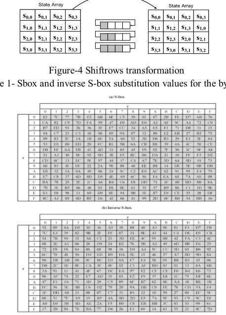
2) ShiftRows(): ShiftRows() processes the State by cyclically shifting the last three rows of the State by different offsets.It is shown in figure 4.
s0,0 s0,1 s0,2 s0,3
s1,0 s1,1 s1,2 s1,3 s2,0 s2,1 s2,2 s2,3
s3,0 s3,1 s3,2 s3,3
State Array
s0,0 s0,1 s0,2 s0,3
s1,1 s1,2 s1,3 s1,0 s2,2 s2,3 s2,0 s2,1
s3,3 s3,0 s3,1 s3,2
State Array ShiftRows
[image:5.612.188.417.240.559.2]Figure-4 Shiftrows transformation
Table 1- Sbox and inverse S-box substitution values for the bytes xy
3) MixColumns(): MixColumns() takes all the columns of the State and mixes their data, independently of one another.The MixColumns transformation can be expressed as a matrix multiplication as shown below and MixColumn transformation is shown in figure 5.
c c c c c c c c s s s s s s s s , 0 , 0 , 0 , 0 ' , 3 ' , 2 ' , 1 ' , 0 02 01 01 03 03 02 01 01 01 03 02 01 01 01 03 02 c c c c
c s s s s
s 0, 1, 2, 3,
' ,
0 ({02} ) ({03} ) s c s0,c s1,c s2,c s3,c
' ,
1 ({02} ) ({03} )
) } 03 ({ ) } 02
({ 2, 3,
, 1 , 0 ' ,
0c s c s c s c s c
s ({03} 0, 1, ) 2, ({02} 3, )
' ,
1c s c s c s c s c
[image:5.612.225.384.604.656.2]Technology (IJRASET)
s0,0 s0,1 s0,2 s0,3
s1,0 s1,1 s1,2 s1,3
s2,0 s2,1 s2,2 s2,3
s3,0 s3,1 s3,2 s3,3
State Array
s0,0 s0,1 s0,2 s0,3
s1,1 s1,2 s1,3 s1,0
s2,2 s2,3 s2,0 s2,1
s3,3 s3,0 s3,1 s3,2
State Array MixColumns
S0,1
S1,1
S2,1
S3,1
S’0,1
S’1,1
S’2,1
S’3,1
Figure-5 MixColumns Transformation
4) AddRoundKey(): AddRound key() is added to the State using XOR operation.It is shown in figure 6.
Figure-6 Addround key
III. PROPOSED SOLUTION
All scan attacks proposed in literature [1], [2], [14] rely on the possibility for the hacker to observe functional intermediate circuit states via the scan chain. Therefore, countermeasures consist in making the observation of the scan chain outputs non exploitable. In the standard scan-based test mechanism, FFs are replaced by scan flip-flops (SFFs) and are connected so that they behave as a shift register in test mode. The output of one SFF is connected to the input of next SFF. The input of the first FF in the chain is directly connected to an input pin (Scan-In) while the output of the last FF is directly connected to an output pin (Scan-Out).
An additional signal (Scan- Enable) selects whether SFFs have to behave normally or as a shift register. The test procedure is composed of three steps:
1) Test patterns are shifted-in via the scan chain (i.e., by keeping Scan-Enable = 1) for #SFF clock cycles (where #SFF is the number of SFFs in the chain);
2) One or two functional clocks (i.e., Scan-Enable = 0) are applied to capture the circuit’s response. Usually, one clock cycle is used for static faults, while two (or even more) clock cycles are used for dynamic faults;
3) The content of SFFs is shifted out for #SFF clock (again, with Scan-Enable = 1) to allow the ATE to compare the obtained values with respect to the expected ones.
The principle of the approach proposed in this brief is to compare the actual responses with the expected ones within the chip boundaries instead of scanning-out the actual responses and comparing it within the ATE. In order to guarantee that secure data cannot leak outside the chip, the output of the comparison is not bitwise delivered to the ATE, but only after applying and comparing the whole test vector (i.e., after comparing the value of each SFF). Therefore, a potential attacker can no longer observe the FFs’ content but simply pass/fail information for the whole test vector.
The general scheme of the proposed Secure Comparator is shown in Figure 7. Instead of directly shifting DUT’s responses (Sout) out of the chip, the ATE also provides the expected responses using the Sexp pin and the actual test response is on-chip compared with the expected one. After having compared all #SFF bits captured in the scan chain, the signal TestRes is asserted if the whole test vector matches the one with expected values. The Secure Comparator is composed of three parts: the Sticky
Technology (IJRASET)
based approach. The Sticky Comparator performs a bitwise serial comparison between the bitstream coming from Sout and the one from Sexp.
Figure-7 Secure Comparator.
An FF (the flag in the figure) is initially reset and then it rises to “1” whenever one comparison fails. The reset of the flag is performed when the scan operation is not enabled (i.e., Sen = “0”). This means then when the circuit goes from capture to test mode, the flag becomes meaningful and its value designates whether the two bitstreams are equal or not. The Output Enabler permits the observation of the TestRes only after comparing the whole test vector. It is composed of a down counter with parallel load that loads the value #SFF whenever the scan operation is not enabled. Therefore, when the circuit goes to test mode, it starts counting and after #SFF clock cycles its terminal
count allows outputting the TestRes signal through the AND gate.
The I/O Buffers allow sharing the same pin for Sin and TestRes. A classical scan-based design requires three signals: scan-in, scanout, and scan-enable. The proposed solution requires, besides Sin and Sen, the Sexp signal (that replaces Sout) and the additional TestRes. However, Sin and TestRes are not used at the same time; therefore, it is possible to use bidirectional buffers shared between them, as shown in Figure 7.
During the shift operation the pin can be set as input and used by the tester to feed the circuit with the input vectors, whereas during the capture operation the pin is activated as output to deliver the previous comparison result. Concerning the area cost, an on-chip comparison is necessary for sensitive scan chains only (the others can be treated in the usual way). However, while the Sticky Comparator is required for every scan chain, all sensitive chains can share the same counter of the Output Enabler. For a DUT with S scan chains, the longest one being composed of #SFFs, this Secure Comparator requires:
1) S flip flops and 2·S logic gates (XOR + OR) for the Sticky Comparator;
2) one counter able to count from Log2(#SFFs) to zero, and S NAND gates to filter the TestRes signals; 3) 2·S buffers.
For example, a circuit with 32 scan chains of 10 000 SFFs each has an extra cost of 32 FFs, 98 combinational gates, 64 buffers, and one 14-bits counter. This overhead represents a negligible cost compared to the size of a circuit. This solution does not impact the standard design flow. The secure comparator can be synthesized and connected to the Sout signals after circuit’s synthesis and DfT insertion, without any modification to the DUT. The same applies when the test data compression mechanisms are used to reduce the test time. In fact, since the Secure Comparator is a stand-alone module that is simply inserted after the DUT’s scan-out, it can be placed downstream of the test response compactor.
IV. GENERAL PRINCIPLE OF SCAN-BASED ATTACK
The general principle of the scan attacks consists in observing the data stored in the round-register after the execution of the first round for several known plaintexts by means of scan-out operations, and then, from these observations, to derive the secret key. For this purpose the principle of the attack proposed in since it will serve as a basis for the proposed attacks.
The attack relies on three requirements:
1) The possibility to switch from mission mode to test mode, which allows the attacker to “stop” the cipher operation at any moment (typically after the first round);
Technology (IJRASET)
by means of scan out;
3) Resetting the circuit and performing one AES round with a first plaintext and doing the same operations with another plaintext only affect the FFs belonging to the round register.
In other words only the round-register FFs depends on the plaintext value after the first round. If these requirements are fulfilled, then the procedure to retrieve the information is performed by the following steps: 1) reset the circuit and process a plaintext for a single round, 2) switch to test mode and scan out the response F, 3) reset the circuit and encrypt another plaintext, 4/ switch to test mode and scan out the response F’. Since only FFs belonging to the round-register may have their value changed between step 2 and 4 (due to third requirement), one can determine for instance some of the FFs of the round-register amongst all the FFs of the design by comparing the two scan responses. For example, if the first scan-out sequence is 01001100011001... and the second one is 00011101011000..., one can infer that the 2nd, 4th, 8th and the 14th FFs belong to the round-register. Actually, for the attack described in and the ones presented in this paper, there is no need to locate the FFs belonging to the round-register, because key retrieval is performed by examining the difference (Hamming distance) between the two scan-out contents F and F’. Since the FFs that do not belong to the round-register are not supposed to flip between two plaintexts, they do not affect the Hamming distance value. This feature permits the attacker to calculate the Hamming distance without caring about which FFs correspond to the AES ones. It must be noticed that the Hamming distance is the same as before the AddRound Key operation i.e. the dependence on the round-key is thus eliminated from the observation when the attack is differential. Besides of removing the effects of the round-key, working in differential mode also permits the division of the AES round in 16 independent datapaths, since when changing an AES input corresponding to one MixColumns and keeping the inputs corresponding to the other MixColumns constant will lead to changes only in the 32 output bits of the MixColumns which input has changed, thus the 96 bits from the other MixColumns outputs keep constant and are eliminated by the Hamming distance. Indeed each byte of the main key may be retrieved while analyzing the output of its respective MixColumns block, and thus for the 16 bytes of the key the attack may be performed independently. This is the main aspect responsible for the reduction of the complexity of the AES round, allowing the scan attacker to quickly retrieve the secret. The attack described in uses the same base previously described, however it relies on an analysis of the distribution of the Hamming distances between F and F’. In order to have the Hamming distances the input pairs are chosen as a and a’=a⊕1 (one pair element differs from the other just at the least significant bit). Since the attack is performed for each byte of the key the length of a is a byte, and so the total number of pairs is 128 (256 input vectors). Then the attacker must find one Hamming distance between 9, 12, 23 or 24, which are generated by only one input pair. Each one of these special hamming distances has a constant pair of b), thus the subkey is K1s=a⊕b or K2s=a⊕b⊕1. The same process is performed on the other 15 bytes of the input for retrieving the other 15 bytes of K. The final choice between the K1s and K2s can be done by checking an encryption result with respect to the 216 possibilities.
V. SECURITY, TESTABILITY
This section discusses the security improvements related to the observation of a single pass/fail result as well as issues related to test.
A. Security Analysis
The role of the proposed Secure Comparator is to avoid the observation of SFFs containing secret information. If the result of the comparison was accessible at each clock cycle instead of each test vector, an attacker could easily observe the scan chain content by shifting in “000…000” on the Sexp pin. Each bit-comparison would then validate that either the actual bit was “0” when TestRes = 1 and vice versa. On the contrary, with the proposed vector-wise comparison, the only way to retrieve the sensitive data information is to apply a brute-force attack by trying every possible response until TestRes is asserted.
This attack would thus require 2#SFF attempts.
If other attacks such as side-channel attacks [16] or faults attacks [17] are dreaded, the Secure Comparator has to be protected as the rest of the circuit. Even if countermeasures can lead to a large area overhead (e.g., [18]) their implementation concerns a very small part of the circuit.
B. Testability
Technology (IJRASET)
classical ATE-based test scheme. Therefore, the achievable fault coverage is not altered. Test time is not increased either, since the expected responses are scanned-in at the same time as the next input vector is scanned-in. Concerning the test of the Secure Comparator itself, any DfT technique controlled by the external ATE (e.g., a dedicated scan chain to test the counter of the Output Enabler) would jeopardize the overall security.
Nevertheless, the Secure Comparator can be totally tested by using only its inputs (Sen, Sexp, Sin, TestRes). We have identified a procedure to test all stuck-at faults no matter of the size of the Secure Comparator. This functional test involves the comparison of the actual SFF values with a partially matching, a fully unmatching, and a correct response. Moreover, it includes the application of a two unmatching responses without the intermediate capture cycle, and twice the execution of the capture cycle. This test procedure requires 6· (#SFF+1) clock cycles to provide 100% stuck at fault coverage.
The area overhead of secure comparator is very low as compared to the other techniques. It is shown in below table 2. Table-2 Area overhead for secure comparator
A limitation of our technique is related to the presence of possible unpredictable values in the SFFs. Computing expected values for the on-chip comparison is indeed no longer possible. To fix this limitation, the Sticky Comparator should ignore the comparison result (and keep unchanged its flag) when Sout is unknown.
Figure-8 Sticky Comparator with masking.
This can be implemented by providing an additional mask signal that is asserted when needed. However, an attacker must not be able to mask as many bits as wanted. In fact, if it were possible to mask all but one bit, it would be obvious to discover the value of each single bit in the scan response. This would reduce the complexity of the brute-force attack from exponential [O(2#SFF)] to linear [O(#SFF)]. Therefore, the number of masked bit (per test vector) must be limited to P such that a brute force attack on 2#SFF−P remains unfeasible. The extra cost to tolerate unknown values includes an extra pin for the mask, a log2 P counter to limit the number of masked bits and two logic gates. Figure 8 shows a possible implementation.
VI. CONCLUSION
Technology (IJRASET)
method can be implemented after building the scan chains, and therefore it can be applied to IP cores as well.
REFERENCES
[1] B. Yang, K. Wu, and R. Karri, “Secure scan: A design-for-test architecture for crypto chips,” IEEE Trans. Comput.-Aided Design Integr.Circuits Syst., vol. 25, no. 10, pp. 2287–2293, Oct. 2006.
[2] B. Yang, K. Wu, and R. Karri, “Scan based side channel attack on dedicated hardware implementations of data encryption standard,” in Proc. IEEE Int. Test Conf., Oct. 2004, pp. 339–344.
[3] Y. Wu and P. MacDonald, “Testing ASICs with multiple identical cores,”IEEE Trans. Comput.-Aided Design Integr. Circuits Syst., vol. 22, no. 3, pp. 327–336, Mar. 2003.
[4] K. J. Balakrishnan, G. Giles, and J. Wingfield, “Test access mechanism in the quad-core AMD opteron microprocessor,” IEEE Design Test Comput., vol. 26, no. 1, pp. 52–59, Jan. 2009.
[5] D. Andreu, “System and method for wirelessly testing integrated circuits,”U.S. Patent 0 244 814, Oct. 6, 2011.
[6] F. Poehl, M. Beck, R. Arnold, J. Rzeha, T. Rabenalt, and M. Goessel,“On-chip evaluation, compensation and storage of scan diagnosis data,” IET Comput. Digit. Tech., vol. 1, no. 3, pp. 207–212, 2007.
[7] G.-M. Chiu and J. C.-M. Li, “A secure test wrapper design against internal and boundary scan attacks for embedded cores,” IEEE Trans. Very Large Scale Integr. (VLSI) Syst., vol. 20, no. 1, pp. 126–134, Jan. 2012.
[8] K. Rosenfeld and R. Karri, “Attacks and defenses for JTAG,” IEEE Design Test Comput., vol. 27, no. 1, pp. 36–47, Jan. 2010.
[9] C. J. Clark, “Anti-tamper JTAG TAP design enables DRM to JTAG registers and P1687 on-chip instruments,” in Proc. IEEE Int. Symp. Hardw.-Oriented Security Trust, Jun. 2010, pp. 19–24.
[10] D. Hely, F. Bancel, N. Berard, M. L. Flottes, and B. Rouzeyre, “Test control for secure scan designs,” in Proc. IEEE Eur. Test Symp.,May 2005, pp. 190–195. [11] D. Hely, M.-L. Flottes, F. Bancel, B. Rouzeyre, N. Berard, and M. Renovell,“Scan design and secure chip [secure IC testing],” in Proc. IEEE Int. On-Line Test. Symp., Jul. 2004, pp. 219–224.
[12] G. Sengar, D. Mukhopadhyay, and D. R. Chowdhury, “Secured flipped scan-chain model for crypto-architecture,” IEEE Trans. Comput.-Aided Design Integr. Circuits Syst., vol. 26, no. 11, pp. 2080–2084, Nov. 2007.
[13] H. Fujiwara and M. E. J. Obien, “Secure and testable scan design using extended de Bruijn graphs,” in Proc. Asia South Pacific Design Autom. Conf., 2010, pp. 413–418.
[14] J. Da Rolt, G. Di Natale, M.-L. Flottes, and B. Rouzeyre, “New security threats against chips containing scan chain structures,” in Proc. IEEE Int. Symp. Hardw.-Oriented Security Trust, Jun. 2011, pp. 110–115.
[15] L. Chunsheng and Y. Huang, “Effects of embedded decompression and compaction architectures on side-channel attack resistance,” in Proc. IEEE VLSI Test Symp., May 2007, pp. 461–468.
[16] P. Kocher, J. Jaffe, and B. Jun, “Differential power analysis,” in Proc. Int. Cryptol. Conf. Adv. Cryptol., 1999, pp. 388–397.
[17] P. Dusart, G. Letourneux, and O. Vivolo, “Differential fault analysis on A.E.S,” in Applied Cryptography and Network Security, vol. 2846. New York, NY, USA: Springer-Verlag, 2003, pp. 293–306.