Abstract
In this study, we present a bilayer resistive switching memory device with Pt/Ta2O5/HfO2-x/Hf structure, which shows sub-1μA ultralow operating current, median switching voltage, adequate ON/OFF ratio, and simultaneously containing excellent self-rectifying characteristics. The control sample with single HfO2-xstructure shows
bidirectional memory switching properties with symmetrical I–V curve in low resistance state. After introducing a 28-nm-thick Ta2O5layer on HfO2-xlayer, self-rectifying phenomena appeared, with a maximum self-rectifying ratio (RR) of ~4 × 10³observed at ±0.5 V. Apart from being a series resistance for the cell, the Ta2O5rectifying layer also served as an oxygen reservoir which remains intact during the whole switching cycle.
Keywords:RRAM, Crossbar, Leakage current issue, Self-rectifying
Background
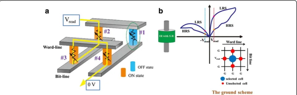
The long time issue faced by semiconductor industry was searching for efficient methods to overcome the fundamental scaling limits of charge-based information storage devices. One of the promising methods is to use crossbar architecture to increase integration density. However, the sneak-path issue (shown in Fig. 1a) acts as a disturbing problem in reading the correct information [1]. Various methods are developed to settle this urgent problem, including one MOSFET transistor-one resistor (1T1R), one diode-one resistor (1D1R), complementary resistive switch (CRS), one bidirectional selector-one resistor (1S1R), and one resistor with self-rectification (1R with S-R) [2]. Among these candidates, resistance random access memories (RRAMs) with self-rectifying characteristics in the low resistance state (LRS) has been receiving great attention in recent years owing to the feasibility of its realization in a simple one resistor struc-ture. Typical bipolar resistive switching (RS) behavior of 1R with S-R cells, as indicated in Fig. 1b, reveals an asymmetric I–V characteristics in the LRS, which means
that electrons can be easily injected or seriously blocked under different bias voltage. In this case, the ground scheme, where the selected word line (WL) is biased to Vread and all other WL/bit lines (BLs) are grounded, is generally adopted to mitigate leakage current (shown in lower right inset of Fig. 1b). The wealth of self-rectifying phenomena in different structures reported so far, while either too high switching voltage [3, 4] or insufficient ON/OFF window [5, 6] is exposed by most reports.
Presented in this work, therefore, is a material system that can provide ultralow operating current (<1 uA), sufficient ON/OFF window (~102), median operating voltages (<6 V), as well as excellent self-rectifying func-tionality (RR >1000). In the bilayer stack, stoichiometric Ta2O5 and anoxic HfO2-x were employed to be electro-lytes, which contacted with high-work-function metal (Pt, 5.6 eV) and low-work-function metal (Hf, 3.9 eV), respectively [7]. The method can be generally stated as one layer (in this case, HfO2-x) and works as the RS layer by trapping and detrapping the deep trap sites while the other dielectric layer (in this case, Ta2O5) remains intact during the whole switching cycle and creates a high Schottky barrier with Pt to constitute the rectifying functionality.
* Correspondence:[email protected]
1Department of Micro/Nano Electronics, Key Laboratory for Thin Film and
Micro Fabrication of Ministry of Education, Shanghai Jiao Tong University, Shanghai, China
Full list of author information is available at the end of the article
Methods
We fabricated the Pt/Ta2O5/HfO2-x/Hf devices by com-bining DC magnetron sputtering and oxygen plasma oxi-dation. The relevant fabrication process flow, equivalent schematic diagram, and cross sectional SEM image in-cluding relevant XPS data of our optimal sample are shown in Fig. 2. A bilayer of Ti and Hf, with a thickness of 3 and 60 nm, respectively, was deposited by DC magne-tron sputtering on a SiO2/Si substrate. The HfO2-x films
were formed by directly oxidizing the metal Hf via oxygen plasma with the power of 50 W and different durations (i.e., 1300, 1600, and 1900 s). Whereas the 28-nm-thick Ta2O5 films were deposited by DC reactive magnetron sputtering using a Ta target in Ar/O2 gas mixture (with excess volume of O2gas) at room temperature, the total pressure was ~0.28 Pa. For the electrode preparation, a large part of fresh metal Hf was reserved by covering aluminum foil in advance, and then the rest part was over-laid by inert Pt (30 nm) to fabricate the bottom-electrode Hf, while top-electrode Pt (50 nm) with a diameter of ~200 μm was deposited by DC magnetron sputtering using a metal shadow mask. For comparison, the stacks of
Pt/HfO2-x/Hf without Ta2O5layer and Pt/Ta2O5(28 nm)/ Hf without HfO2-xlayer were also fabricated.
The cross sectional image was observed using a UKTRA-55 field emission scanning electron microscope (FESEM); and chemical status of films were examined using an X-ray photoelectron spectroscopy (XPS, Kratos Axis UltraDLD spectrometer, Kratos Analytical-A Shimadzu group com-pany). For the XPS measurement, the Ar + ion beam en-ergy was set to 1 keV during the sputter-etching. As to the electrical measurements, a low-noise Keithley 4200 semi-conductor characterization system was conducted at room temperature, in voltage sweep mode. Each voltage sweep began from 0 V, and the bias was applied to the TE while the BE was grounded.
[image:2.595.58.539.88.242.2]Results and Discussion
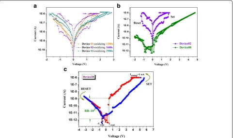
Figure 3 shows the typical I−V characteristics of our sam-ples (deposited in the same batch). For simplicity, the de-vice that possesses Pt/HfO2-x/Hf stack but different
oxidizing duration (i.e., 1300, 1600, and 1900 s) is denoted as Device01, Device02, and Device03, respectively. Whereas Device00 and Device28 denote Pt/Ta2O5/Hf Fig. 1aThe sneak-path issue happened in crossbar structure andbtypical I–V characteristics and read scheme of 1R with S-R cells
Fig. 2aFabrication process flow for Pt/Ta2O5/HfO2-x/Hf stack.bSchematic of device layout and the electrical measurement configuration.c
Typical FESEM cross sectional images of the Ta2O5(28 nm)/HfO2-x(oxidizing 1600 s)/Hf stack, along with its XPS data of each oxide layer
(stoichiometric Ta2O5and anoxic HfO2)
[image:2.595.58.540.563.692.2]stack and the sample with Pt/Ta2O5(28 nm)/HfO2-x
(oxi-dizing1600s)/Hf structure, respectively. As indicated in Fig. 3a, Device02 behaved better bidirectional RS charac-teristics than Device01 and Device03; therefore, this condi-tion was chosen to prepare the RS layer in our Pt/Ta2O5/ HfO2-x/Hf devices. Whereas rectifying properties (no RS
behavior) was found in Device00, and the effect of their combination was reflected by Device28 (Fig. 3c). Addition-ally, it is worth noting from the XPS results in Fig. 2c that the binding energy of Ta 4f well coincided with the re-ported value of the Ta 4f peak (26.6 eV for Ta 4f7/2 and 28.4 eV for Ta 4f5/2) in Ta2O5[3, 8]. For HfO2-x, grown by
directly oxidizing the metal Hf via oxygen plasma with a duration 1600 s, the core-level Hf4f7/2–Hf4f5/2 was ob-served at an energy corresponding to the non-stoichiometric HfO2 (12.7–18.5 eV) [9], which indicated the presence of the neutral oxygen vacancy in our HfO2-x layer. Along with the I–V characteristics in Fig. 3, it was confirmed that HfO2-xlayer plays the role of RS layer
in-deed, whereas stoichiometric Ta2O5layer works as a recti-fier with high resistance and only slight oxygen deficiency. Beyond that, the thickness of HfO2-x layer with oxidizing
duration 1600 s approximates 30 nm.
When a positive voltage sweep with anIcompof 1 uA (to prevent the device hard breakdown) were firstly applied whereas their BE were grounded, then as-fabricated
devices transform into the LRS (or ON state), i.e., the SET process (for Device02 and Device28). Particularly the elec-troforming was relieved since a large amount of oxygen vacancies (VO) in the HfO2-x film (RS layer) [10, 11]. To
turn the devices back into the HRS, i.e., the RESET process, a negative voltage sweep (−1.5 V for Device02 and−3.5 V for Device28) was required. Particularly, after stacking a 28-nm-thick Ta2O5layer on HfO2-xfilm, a pro-nounced self-rectifying behavior appeared in Device28. Significantly, a ~4 × 10³-fold reduction in LRS current was observed at−0.5 V(−Vread) compared with the current at 0.5 V(Vread). In addition, a DC cycling and retention prop-erty test of Device28 were also implemented, the results are presented in Fig. 4. The high uniformity of RS per-formance and stable distribution of retention time data (baked at 85 °C up to 104s) indicate the high feasibility of the present structure as the RS element in crossbar.
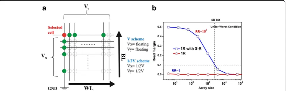
To demonstrate the feasibility of settling the sneak-path issue by utilizing the observed self-rectifying behavior, nu-merical simulation of the maximum crossbar size has also been conducted for Device28 by the use of MATLAB. Figure 5 shows that the obtained self-rectifying property in this work can guarantee a maximum crossbar array size of
∼5 k bit in the worst case scenario for reading (V scheme). Now, we turn to discuss the switching and self-rectifying mechanism discovered in Device28 from the Fig. 3The semi-logarithmic I-V curves ofaDevice01-03 (different oxidizing duration),bDevice02 (violet curve) and Device00 (green curve), andc
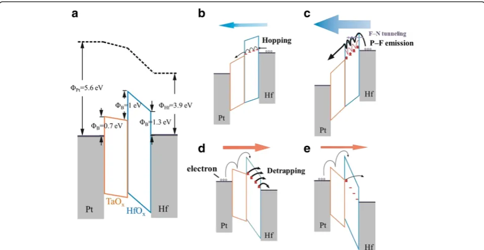
[image:3.595.58.544.88.374.2]viewpoint of energy band. Although the accurate energy band structure could not be depicted due to the lack of precise information on the band offset between the two dielectric layers and possible (larger) Schottky barrier at the HfO2-x/Hf interface, a tentative schematic band
dia-gram could be drawn as shown in Fig. 6a for the zero external bias condition. Here, the CB offset between Ta2O5 and HfO2-x was taken as 1 eV considering the
known electron affinities of both materials [12, 13], and contact potential at the HfO2-x/Hf interface was taken as
1.3 eV based on their electron affinity and work func-tion. As the band gap of Ta2O5 is lower than that of HfO2-x (≈4.2 and ≈5.68 eV, respectively) [3], the
elec-trons transported to Ta2O5 easily moved to Pt TE via the conduction within the CB of the Ta2O5layer, so that the Ta2O5layer kept intact under the positive bias condi-tion. In addition, considering the high oxygen affinity of beneath metal Hf in the HfO2-x/Hf stack, abundance of VOwould be induced in bulk portion of HfO2-x.It is be-lieved that these VO values were dispersed within the HfO2-x layer and acted as the deep trap sites (red dot
lines drawn in Fig. 6b–e) for the injected carriers in both states [3]. (It must be noted that the trap depth of 1.0 eV well coincided with the energy distance between the Vo and the CB edge in HfO2-x [14]. Therefore, the trap
positions of HfO2-xlayer occur near Ecof Ta2O5layer.) When a small positive bias was applied to the Pt TE, a small amount of injected electrons, which tunneling from cathode to traps, were interfered with by the deep trap and transported through the HfO2-x via hopping
mechanism, so that the current flow under this circum-stance must be much lower, as schematically shown in Fig. 6b. The observation of initially low current in Fig. 3b suggests that the deep trap levels were with the trap-empty configurations under low positive bias condition, which well coincided with the HRS. As the positive volt-age increased, the carrier injection became higher and the energy band of electrolytes would be tilted further, so that traps started to be filled with major injected car-riers, and the others would tunnel from Hf BE to the Ec of HfO2-x layer (F-N tunneling). Actually, the subsequent
emission from traps to the Ecof HfO2-xlayer is essentially Fig. 4aDistribution of the ILRS(at ±0.5 V) under DC sweeping mode for Device28 andbits retention property
Fig. 5aSchematic of data reading (V, V/2) andbcomparison of calculated readout margins inN × Ncrossbar array integrating RRAM cells with and without self-rectifying behavior
[image:4.595.61.540.88.229.2] [image:4.595.59.540.550.704.2]the Poole–Frenkel emission [15]. At the same time, the whole system switched to LRS (as indicated in Figs. 3b and 6c). The switching back from the LRS to HRS under the negative bias could be understood as follows.
After withdrawing the positive bias and applying a negative bias to the Pt TE, the electrons in the HfO2-x
traps started to detrap continually while the electron injection from the Pt TE was suppressed by the high Schottky barrier height, Fig. 6c shows the schematic diagram of this circumstance. When the traps became empty by the high negative bias, and bias was removed subsequently, the energy band diagram could be repre-sented by Fig. 6e.
The most critical feature of the abovementioned switching mechanism is the change in the charge state of the electron traps, presumablyVO with different oxi-dation states in HfO2-x, not the variations in their local spatial distribution or concentration. Note that it is hopeful that improve the rectifying properties of our de-vice if its active area can scaling further.
Conclusions
In summary, the RRAM device with ultralow operating current (<1 uA), sufficient ON/OFF ratio (~102), median operating voltages (<6 V), as well as excellent self-rectifying properties was prepared in a simple Pt/ Ta2O5/HfO2-x/Hf structure successfully. And
satisfac-tory switching uniformity and retention performance are also demonstrated in it. In the stack, Ta2O5 layer
works as a rectifier with high resistance and only slight oxygen deficiency, while HfO2-x layer plays the role of the RS layer with more oxygen deficiency, lower dielec-tric constant, and higher energy band gap. These abovementioned merits manifest that the prototype Pt/ Ta2O5/HfO2-x/Hf devices could be used to effectively
mitigate the sneak leakage in crossbar RRAM arrays.
Acknowledgements
The authors thank the Instrumental Analysis Center of Shanghai Jiao Tong University and Key Laboratory of Microelectronics Devices & Integrated Technology, Institute of Microelectronics of Chinese Academy of Sciences.
Funding
There is no funding source for this work.
Authors’Contributions
HM and JF designed the experiments. HM and TG carried out the experiments. HM wrote the manuscript. JF and HL provided suggests for the experimental results analyzing and helped amend the manuscript. XX, QL, TG, and PY helped for the electrical tests and developed relevant analysis tools. All authors read and approved the final manuscript.
Competing Interests
The authors declare that they have no competing interests.
Author details
1Department of Micro/Nano Electronics, Key Laboratory for Thin Film and
Micro Fabrication of Ministry of Education, Shanghai Jiao Tong University, Shanghai, China.2Key Laboratory of Microelectronics Devices and Integrated
Technology, Institute of Microelectronics, Chinese Academy of Sciences, Beijing, China.
[image:5.595.58.537.87.334.2]Received: 21 November 2016 Accepted: 6 February 2017
References
1. Chang SH, Lee SB, Jeon DY, Park SJ, Kim GT, Yang SM, Chae SC, Yoo HK, Kang BS, Lee MJ, Noh TW (2011) Oxide double-layer nanocrossbar for ultrahigh-density bipolar resistive memory. Adv Mater 23:4063 2. Pan F, Gao S, Chen C, Song C, Zeng F (2014) Recent progress in resistive
random access memories: materials, switching mechanisms, and performance. Mater Sci Eng RRep 83:1
3. Yoon JH, Song JS, Yoo IH, Seok JY, Yoon KJ, Kwon DE, Park TH, Hwang CS (2014) Highly uniform, electroforming-free, and self-rectifying resistive memory in the Pt/Ta2O5/HfO2-x/TiN structure. Adv Func Mater 24:5086 4. Li YT, Jiang XY, Tao CL (2013) A self-rectifying bipolar rram device based on
Ni/HfO2/N(+)-Si structure. Modern Phys Lett B 28:389
5. Wang YF, Hsu CW, Wan CC, Wang IT, Lai WL, Chou CT, Lee YJ, Hou TH (2014) Homogeneous barrier modulation of Ta2O5/TiO2bilayers for ultra-high endurance three-dimensional storage-class memory. Nanotechnology 25:165202
6. Kwon JY, Park JH, Kim TG (2015) Self-rectifying resistive-switching characteristics with ultralow operating currents in SiOxNy/AlN bilayer devices. Appl Phys Lett 106:223506
7. Michaelson HB (1977) The work function of the elements and its periodicity. J Appl Phys 48:4729
8. Song WD, Ying JF, He W, Zhuo VY-Q, Ji R, Xie HQ, Ng SK, Serene LG-NG, Jiang Y (2015) Nano suboxide layer generated in Ta2O5by Ar+ion irradiation. Appl Phys Lett 106:031602
9. Kruchinin VN, Aliev VSH, Perevalov TV, Islamov DR, Gritsenko VA, Prosvirin IP, Cheng CH, Chin A (2015) Nanoscale potential fluctuation in non-stoichiometric HfOx and low resistive transport in RRAM. Microelectronic Eng 147:165 10. Tyapi P (2011) Ultrathin Ta2O5film based photovoltaic device. Thin Solid
Film 519:2355
11. Cho B, Song S, Ji Y, Lee T (2010) Electrical characterization of organic resistive memory with interfacial oxide layers formed by O2plasma treatment. Appl Phys Lett 97:063305
12. Zeng W, Bowen KH, Li J, Dabkowska I, Gutowski M (2005) Electronic structure differences in ZrO2vs HfO2. J Phys Chem A 109:11521 13. Lai BC-M, Kung N-H, Lee JY-M (1999) A study on the capacitance–voltage
characteristics of metal-Ta2O5-silicon capacitors for very large scale integration metal-oxide-semiconductor gate oxide applications. J Appl Phys 85:4087
14. Gavartin JL, Ramo DM, Shluger AL, Bersuker G, Lee BH (2006) Negative oxygen vacancies in HfO2as charge traps in high-k stacks. Appl Phys Lett 89:082908
15. Wong H-SP, Lee HY, Yu S, Chen YS, Wu Y, Chen PS, Lee B, Chen FT, Tsai MJ (2012) Metal–oxide RRAM. Proc IEEE 100:1951
Submit your manuscript to a
journal and benefi t from:
7Convenient online submission
7Rigorous peer review
7Immediate publication on acceptance
7Open access: articles freely available online
7High visibility within the fi eld
7Retaining the copyright to your article
Submit your next manuscript at 7 springeropen.com