N A N O E X P R E S S
Open Access
Enhancement of a-IGZO TFT Device
Performance Using a Clean Interface
Process via Etch-Stopper Nano-layers
Jae-Moon Chung
1,2, Xiaokun Zhang
1, Fei Shang
1,2, Ji-Hoon Kim
2, Xiao-Lin Wang
2, Shuai Liu
1, Baoguo Yang
2,3and Yong Xiang
1*Abstract
To overcome the technological and economic obstacles of amorphous indium-gallium-zinc-oxide (a-IGZO)-based display backplane for industrial production, a clean etch-stopper (CL-ES) process is developed to fabricate a-IGZO-based thin film transistor (TFT) with improved uniformity and reproducibility on 8.5th generation glass substrates (2200 mm × 2500 mm). Compared with a-IGZO-based TFT with back-channel-etched (BCE) structure, a newly formed ES nano-layer (~ 100 nm) and a simultaneous etching of a-IGZO nano-layer (30 nm) and source-drain electrode layer are firstly introduced to a-IGZO-based TFT device with CL-ES structure to improve the uniformity and stability of device for large-area display. The saturation electron mobility of 8.05 cm2/V s and theVthuniformity of 0.72 V are realized on the a-IGZO-based TFT device with CL-ES structure. In the negative bias temperature illumination stress and positive bias thermal stress reliability testing under a ± 30 V bias for 3600 s, the measuredVth shift of CL-ES-structured device significantly decreased to−0.51 and + 1.94 V, which are much lower than that of BCE-structured device (−3.88 V, + 5.58 V). The electrical performance of the a-IGZO-based TFT device with CL-ES structure implies that the economic transfer from a silicon-based TFT process to the metal oxide semiconductor-based process for LCD fabrication is highly feasible.
Keywords:Displays, a-IGZO, Thin film transistors, Etch-stopper, Reproducibility, Reliability
Background
Thin film transistor (TFT) backplane with higher resolution and larger panel size is highly desired in the flat plane display industry. Semiconductor material with a high electron mobility is crucial to improve the per-formance of TFT backplane. In particular, a metal oxide semiconductor-based TFT backplane is considered as a promising candidate to overcome the limitation of silicon-based TFT backplane in terms of mechanical flexibility and electron mobility [1–4]. Although a metal oxide semiconductor-based TFT backplane shows prom-ising properties, the process method with a low-cost process for both large-scale deposition for industrial application is still needed [5].
Amorphous indium-gallium-zinc-oxide (a-IGZO) is an excellent metal oxide semiconductor with a high saturation electron mobility (~ 5–10 cm2/V s) and a low off-current (< 10 pA) [6–10]. The common industrial production method for a-Si:H-based TFT backplane is five-mask-back-channel-etched (BCE) process. However, a-IGZO nano-film has a very low chemical resistance to the typical etchants currently used in the BCE process. Especially, a-IGZO nano-films would be completely etched in few seconds when they are exposed to Al etch-ant composed of phosphoric acid, nitric acid, and acetic acid [11–13]. This uncontrollably fast etching hinders the adoption of BCE process for a-IGZO-based TFT backplane. To utilize a-IGZO in BCE-structured back-plane, Cu wiring technology has been developed, as the etchant used in Cu wiring process, which is based on H2O2, is much milder to a-IGZO nano-film than the
ones used in Al wiring [11, 13]. Unfortunately, a-IGZO nano-film is still damaged during Cu wiring process
* Correspondence:[email protected]
1School of Materials and Energy, University of Electronic Science and Technology of China, 2006 Xiyuan Ave, West High-Tech Zone, Chengdu 611731, Sichuan, China
Full list of author information is available at the end of the article
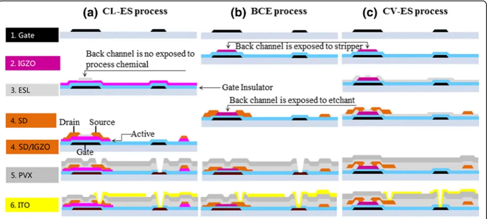
even when milder etchant is used. Even milder etchants cause damage on the surface of a-IGZO nano-film that forms back channel of TFT devices. These damages cause collapse in the stoichiometric molecular compos-ition ratio near the surface of a-IGZO nano-film, leading to the aggravation of uniformity in large-area display and TFT device reliability. To date, conventional six-mask-etch-stopper (CV-ES) process is developed to fabricate a-IGZO-based TFT backplane with etch-stopper-layer (ESL) structure [14,15]. However, this six-mask ES process may lead to a negative economic feasibility. Moreover, this increased number of thin film layers would increase the inter-layer overlap area and re-sult in the increased parasitic capacitance and decreased opening ratio [16–18]. Although five-mask ES process that produces TFT backplane using half-tone and lift-off technology has been reported recently, this process is not accessible for the production of a-IGZO-based TFT backplane, as their active layer surface is still exposed to process chemicals such as stripper and photoresist in the last step, which may cause considerable contamin-ation to a-IGZO, thus reducing the device quality and the production yield [19–21]. Therefore, the industrial production method for a-IGZO-based TFT backplane with highly uniformity and stability remains challenging.
In this paper, we propose a clean five-mask ES process (CL-ES) via introducing ESL for fabrication of a-IGZO-based TFT backplane. This newly developed CL-ES process is highly compatible with the existing process for BCE device. This CL-ES process is designed to have the equal masks to that of BCE process, which ensures a negligible loss of productivity of existing AM-LCD TFT backplane FAB. a-IGZO-based backplane produced
using CL-ES process deposits gate insulator, IGZO nano-layer, and ES nano-layer sequentially, then forms a new ESL mask through dry-etch method. This could prevent the contamination of a-IGZO nano-layer and their interface from etchant, stripper, and solvent. This newly formed nano-mask helps improve the uniformity and stability of TFT device. Compared to conventional BCE-structured device, a-IGZO-based device with CL-ES structure shows enhanced electrical performances, namely a higher saturation electron mobility, a high opening ratio, and a low power consumption.
Methods/Experimental
Fabrication of a-IGZO-based TFT Backplane
The a-IGZO-based TFT backplane with ES structure fabricated via CL-ES process was as follows (Fig.1).
Firstly, double layer (Mo/Cu:30 nm/250 nm) was used for gate electrode as it has a reasonably low resistivity. Then, gate insulator, silicon nitride (SiNx)/silicon oxide (SiOx) (300 nm/100 nm), was deposited by plasma-enhanced chemical vapor deposition (PECVD) method. This SiNx film is designed to prevent oxidation of Cu metallizing and diffusion of Cu ion into the gate insula-tor. Subsequently, a SiOx thin film was deposited. The deposition conditions of PECVD SiOx film were 17-KW RF power, 1000 mTorr pressure, 1:55 SiH4/N2O gas
ra-tio, and 350 °C temperature. Then, a-IGZO nano-film was deposited to 30 nm using dc rotary magnetron sput-ter. The target had the diameter of 171 mm while the composition was In2O3:Ga2O3:ZnO = 1:1:1 mol%. The
sputtering parameters for the a-IGZO nano-film were system base pressure of 5~ 9 × 10⁻⁷ Torr, rf sputtering power of 10 KW, sputtering pressure of 5-mTorr Ar/O2
[image:2.595.59.539.499.715.2]gas mixture (85% Ar-15% O2). The deposition
temperature is at room condition. Produced a-IGZO film is annealed at 330 °C for 1 h in clean dry air environment.
Secondly, etch-stopper (ES) nano-layer (SiOx) was deposited using PECVD method. ES nano-layer is simul-taneously deposited to prevent contamination in a-IGZO layer. As in BCE process, there is no protective layer for a-IGZO nano-film before S/D electrode pat-terning process, surface contamination, and damage on a-IGZO nano-film by S/D etchant when forming TFT channel is unavoidable. ES nano-layer in CL-ES process can effectively protect TFT channel from external contamination and damage. The ES nano-layer was de-posited to a thickness of 100 nm. The deposition condi-tions of SiOx thin film were 17-KW RF power, 1000 mTorr pressure, 1:66 SiH4/N2O gas ratio, and
240 °C temperature. The ES nano-mask produced was etched by dry etching and patterning. During the etching process, CF4 and O2 gas were supplied at a
rate of 2000 sccm/800 sccm.
Thirdly, Mo/Cu/Mo was also used for S/D electrode. To select S/D electrode of a-IGZO TFT, the work func-tion difference between metal and a-IGZO was consid-ered to form an Ohmic contact and the low-resistivity materials. As described in the etch-stopper process, dur-ing the patterndur-ing of ES mask, the a-IGZO nano-films, which are not protected by the etch-stopper layer, are already conducted by being bombarded with CF4
plasma. Therefore, Ohmic contact is formed naturally with Mo/Cu/Mo [22]. The S/D layers were deposited in the thickness of 30 nm/300 nm/30 nm with the same sputtering conditions as the gate electrode. In addition, multi-thin film layers of Mo/Cu/Mo and a-IGZO were batch etched using“H2O2based Cu etchant containing a
fluoride additive” to complete the S/D electrode. The 30 nm of Mo added on top of Cu was formed to prevent oxidation of Cu surface by passivation film (SiOx) in the next process and to prevent plasma damage of Cu sur-face, during dry etching for passivation hole formation.
Fourthly, passivation film, divided into two kinds of thin film, was deposited using PECVD method. The first pas-sivation was made of SiOx thin film. The thin film was 250 nm thick. The second passivation constituted of SiNx thin film. The thickness of the thin film was 200 nm.
Fifthly, as the pixel electrode, indium tin oxide (ITO) film, which is most commonly used in the display indus-try, was utilized. The ITO film was 40 nm thick, and dc sputtering was used for the deposition. Then, the final annealing was carried out in a clean dry air environment at 230 °C for 1 h using a hot air oven. The electrical characteristics of manufactured a-IGZO TFTs were measured using Keysight 4082A Parametric Test System. This process will obtain the same number of masks
(TN product standard: five masks) as the BCE process, which is widely used in mass manufacturing.
For comparison, a-IGZO-based TFT backplane with BCE structure was fabricated via BCE process.
Characterization
TFT’s I-V measurement was conducted at room
temperature using a semiconductor characteristic analyzer. The analyzing condition to evaluate the TFT’s stability under negative gate bias temperature illumin-ation stress (NBTIS) was as follows.VgsandVdswere
re-spectively fixed at−30 and 15 V, and the temperature of the substrate was kept at 60 °C. The luminance for NBITS was set at 5000 cd/m2. The duration of the stress for evaluation continued for 3600 s [23]. Positive gate bias thermal stress (PBTS) were tested at a Vgs of 30 V
and aVdsof 15 V, and the substrate temperature was set
at 60 °C. The duration of the stress for evaluation continued for 3600 s [24].
Results and Discussion
a-IGZO-based TFT fabricated via CL-ES process shows the same mask number to that of BCE process (Fig. 1). Compared with a-IGZO-based TFT with BCE structure, a-IGZO-based TFT with CL-ES structure shows two ad-vantages: (1) a-IGZO-based backplane produced using CL-ES process deposits gate insulator, a-IGZO nano-layer, and ES layer sequentially, then forms a ESL nano-mask through dry-etch method. This newly formed ESL nano-mask with 100 nm can prevent the exposure of a-IGZO nano-film to etchant, stripper, or photoresist. Therefore, the contamination at inter-layer interfaces is ef-fectively prevented [25]. (2) At the same time, a-IGZO nano-film is not protected by ES layer but bombarded by CF4 plasma during the ESL nano-mask formation, thus
becomes a conductor. This naturally forms the Ohmic contact between S/D electrode of following process and a-IGZO semiconductor. For another part, a simultaneous etching of S/D and a-IGZO nano-layer can be one overlay allowance of ESL-(a-IGZO+S/D metallization) layer, which could decrease the two overlay process error of the a-IGZO-ESL and ES-S/D metallization layer in the con-ventional ESL process (Fig.2). The overlay number of the a-IGZO, ES, and S/D layer is reduced, which resulted in the decrease in the size of TFT device that lowered the parasitic capacitance. The outcome planar structure is similar to the BCE structure (Fig.3a, b).
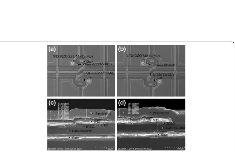
Figure 3 shows the SEM images of a-IGZO-based
Fig. 2(Color online) Schematics of simultaneous formation method for TFT channel and S/D electrode in CL-ES process.aThe first step that forms gate electrode.bThe second step that forms etch-stopper layer.cThe third step that forms S/D photo pattern.dThe fourth step that forms S/D electrode and active pattern
[image:4.595.57.540.87.364.2] [image:4.595.59.541.405.716.2]Meanwhile, a passivation layer can be found on the top of a-IGZO nano-layer in BCE structure (Fig.3d). In the pre-sented CL-ES process, an a-IGZO nano-layer with a thick-ness of 30 nm is deposited. Moreover, the damage during wet etching is negligible. For BCE process, a 70-nm a-IGZO nano-layer is deposited, as a-a-IGZO layer needs compensation for etching loss. The difference between the thicknesses of a-IGZO nano-layers in CL-ES and BCE structures can be observed in the SEM images (Fig.3c, d).
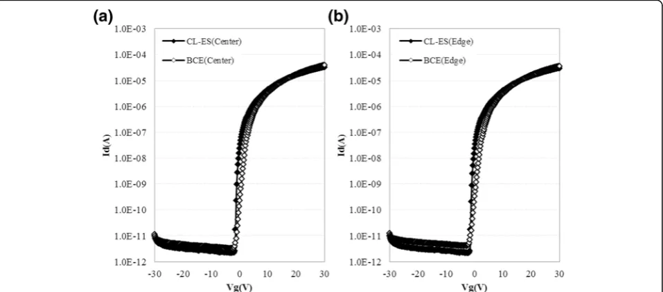
The I-V characteristics of a-IGZO-based TFT with CL-ES structure and BCE structure are compared (Fig. 4). The saturation electron mobility, threshold voltage, sub-threshold voltage swing (SS) value, and more characteris-tic values are summarized in Table1. Note that the values summarized in Table 1 are the average number derived from the center and edge of an 8.5 generation glass sub-strate. The a-IGZO-based TFT with CL-ES structure real-izesVthof−0.8 V, SS value of 0.18 V/dec, and saturation
electron mobility of 8.05 cm2/V s. In the a-IGZO-based TFT with BCE structure, the corresponding results are Vthof + 0.5 V, SS value of 0.77 V/dec, and saturation
elec-tron mobility of 6.03 cm2/V s. Compared to the BCE structure, CL-ES structure shows an improved device per-formances. However, the on-current characteristic of the a-IGZO-based TFT device with CL-ES structure is lower than that with BCE-structured device. This is due to the fact that TFT channel structures are different in CL-ES and BCE structures. Generally, BCE-structured TFT chan-nel length are the distance between S/D metal electrodes, and the measured channel length in this study is 5 um [21]. In CL-ES structure, electrodes are in contact with the a-IGZO nano-film that is stretched at the side of ESL
nano-mask. Therefore, the channel length is decided by the distance between the a-IGZOs defined at the etch-stopper’s sides, but not determined by the distance be-tween the electrodes. The channel length of the present CL-ES-structure device is measured to be 10 um.
As shown in Table1, the measured values ofIon/Ioff
ra-tio (~ 106, see Table 1) are approximately 10 times smaller than the typical value (> 107) of a-IGZO-based TFTs. This is because the measuring equipment used here is for the 8.5 generation mass production. Long ca-bles are necessary for these measurements, as the size of the industrial equipment is large. The long cables re-sulted in an increased measurement noise. In the follow-ing reliability testfollow-ing, smaller-scale measurfollow-ing equipment is utilized, and the individual TFT devices is used as spe-cimen for measurement. In this way, the measured Ion/
Ioffratios are all upper 107(see below).
CL-ES process is carefully designed to prevent a-IGZO channel layer being exposed to etchant, photoresist, or stripper. During the process that produces CL-ES process, gate insulator, a-IGZO nano-layer, and ES nano-layer, each inter-layer interface is in contact with
[image:5.595.305.539.110.194.2]Fig. 4(Color online) Comparison of I-V characteristic of a-IGZO TFTs with CL-ES and BCE structure on the center (a) and edge (b) of 8.5 generation glass substrate
Table 1Comparison of I-V characteristics of a-IGZO-based TFT device with CL-ES structure and BCE structure
Item Unit CL-ES BCE
Vth_Avg V −0.85 + 0.50
Vth_Range V 0.72 2.14
Subthreshold voltage swing V/dec. 0.18 0.77
Ion/Ioffratio – 3.82 × 10⁶ 2.62 × 10⁶
[image:5.595.60.539.491.702.2]only DI water for cleaning purpose. Hence, the chemical contamination is negligible in insulator layer and a-IGZO nano-layer [25, 26]. However, the BCE process not only exposes channel layer to the chemicals but also involves Cu ion diffusion contamination, as the a-IGZO channel is directly exposed to Cu metal. This is also avoided in device with CL-ES structure. The channel re-gion of the a-IGZO nano-film is well protected by ESL nano-mask. The low chemical contamination in CL-ES process may lead to a low carrier trap density at the interface between a-IGZO nano-layer and insulator layer, resulting in an excellent SS value. This low chemical contamination of a-IGZO-based TFT device via CL-ES process also helps improve the uniformity and reprodu-cibility of a-IGZO TFT, which are highly important in industrial production [27,28].
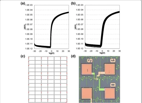
Figure 5 shows the measured I-V characteristic of TFTs with CL-ES structure and BCE structure derived from 42 measuring points on an 8.5 generation sub-strate. a-IGZO-based TFT with CL-ES structure has a Vthrange of 0.72 V, while that of BCE-structured device
is 2.14 V (Table1). In other words, the uniformity of de-vice performance is significantly improved by CL-ES structure.
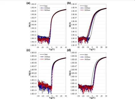
Figure 6a, b show the I-V characteristic shift of CL-ES-structured device and BCE-structured device ob-tained in NBTIS testing, respectively. The NBTIS testing results are summarized in Table2. Under the stress con-dition described in the Table 2, the Vth shift of
CL-ES-structured device and BCE-CL-ES-structured device are −0.51 and −3.88 V, respectively. Additionally, the on-current shift, off-current shift, and SS value variance of the CL-ES-structured device are all lower than those of the BCE-structured device (Table 2); this is because a-IGZO-based device with CL-ES-structure can effectively prevent the contamination of a-IGZO and lower carrier trap density of a-IGZO TFT channel. Especially, when looking at the result from first 1000 s of stress, no SS value change is observed in CL-ES-structured device. This phenomenon is comparable to the 0.16 V/dec in-crease in SS value of BCE-structured device, as it shows that defect sites, which can form carrier traps on the
[image:6.595.57.540.352.703.2]surface of a-IGZO nano-film constituting CL-ES TFT back channel, are not additionally created by electrical and illu-mination stress. These results fully prove that CL-ES-structured device is much more stable than BCE-CL-ES-structured device. Figure6c, d show the I-V curve shift of CL-ES- and BCE-structured TFTs obtained from PBTS testing. The de-tailed PBTS testing results are summarized in Table3. Both CL-ES-structured TFT and BCE-structured TFT have de-creased in ion current during PBTS evaluation. This is caused by the shift inVthto the positive direction. During
PBTS evaluation, residual ion current ratio [(last ion/initial
ion) × 100] of the CL-ES-structured TFT with relatively smallerVthpositive shift (+ 1.94 V) is in the level of 88.2%.
When compared to the BCE-structured TFT's residual ion current ratio of 41.3%, CL-ES-structured TFT is signifi-cantly superior. This shows the important capacity differ-ence during designing of gate drive on array (GOA) circuit. Different from NBTIS, SS value of CL-ES-structured TFT does not have significant variation ((ΔSS 0.06 V/dec), or ra-ther decreases (ΔSS −0.86) like as BCE-structured TFT. This is perhaps due to the carriers, accumulate in the inner space and interface between gate insulator and a-IGZO
[image:7.595.62.537.89.438.2]Fig. 6(Color online) I-V transfer characteristic drift of CL-ES (a,c) and BCE (b,d) TFT obtained from NBITS (a,b) and PBTS testing (c,d)
Table 2The on-current shift, off-current shift, and subthreshold voltage swing variance values of CL-ES-structured device and BCE-structured device
BL T Bias
time
CL-ES BCE
Vgbias−30 V Vgbias−30 V
Ion(uA) Ioff(pA) Vth(V) SS (V/dec) Ion(uA) Ioff(pA) Vth(V) SS (V/dec)
0nit RT 0 s 7.50 0.01 −0.71 0.50 8.79 0.21 2.34 1.69
5000nit 60 °C 1000 s 7.92 0.12 −1.06 0.50 11.83 0.57 0.02 1.85
5000nit 60 °C 3600 s 6.99 0.10 −1.22 0.83 15.99 6.59 −1.54 2.11
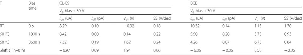
[image:7.595.57.539.636.732.2]nano-film by positive gate bias, filling the carrier trap site at the early stage, causing decrease in carrier trap phenomenon. Moreover, the threshold voltage shift phenomenon occurs by carrier charge trapped near the interface between gate insulator and a-IGZO nano-film. Small threshold voltage shift of CL-ES-structured TFT rep-resents that the interface and the inner space of a-IGZO are remarkably clean. In conclusion, PBTS testing also suggests that CL-ES structure and process lead to a better device reliability.
Conclusions
In conclusion, a newly developed CL-ES process has been successfully developed to fabricate a-IGZO-based TFT back-plane with five masks for advanced display. The CL-ES process has the advantages of an etch-stopper-layer struc-ture while maintaining the equal number of masks and simi-lar device areas to a BCE process, which overcomes the problem of increased mask number and occupied area in conventional etch-stopper TFT devices. A newly formed ESL nano-mask and a simultaneous etching of a-IGZO nano-layer and S/D electrode nano-layer enable a high uni-formity and stability of device for large-area display. In re-spect of electrical performance, the reproducibility and reliability of device performance of a-IGZO-based TFT with CL-ES structure are much better than that of BCE-structured device. The a-IGZO-based TFT device has aVth
distribution over 42 measuring points TFTs on the 8.5 gen-eration glass substrate of 0.72 V, saturation electron mobility of 8.05 cm2/V s, and SS value of 0.18 V/dec. According to reliability evaluation results obtained from NBTIS and PBTS, Vth variances before and after stress of CL-ES
a-IGZO-based TFTs are −0.51 and 1.94 V after 3600 s of stress, respectively. The SS value variances are 0.33 and 0. 06 V/dec. Therefore, by overcoming the technological and economic obstacles, the presented CL-ES technique will pave the way for next-generation high-resolution and large panel display products.
Abbreviations
a-IGZO:Amorphous indium-gallium-zinc-oxide; AM-LCD: Active matrix liquid crystal display; BCE: Back channel etch; ESL: Etch-stopper layer; GOA: Gate drive on array; NBTIS: Negative bias temperature illumination stress; PBTS: Positive bias temperature stress; SiNx: Silicon nitride; SiOx: Silicon oxide; SS: Subthreshold swing; TFT: Thin film transistor; TN LCD: Twisted nematic liquid crystal display
Acknowledgements
The authors appreciate the Chongqing BOE Optoelectronics (CQ1610-PM-IP-001). Y.X. also acknowledges financial support from the Program for New Century Excellent Talents in University (NCET-12-0098).
Funding
This work is supported by Chongqing BOE Optoelectronics (CQ1610-PM-IP-001). Y.X. also acknowledges financial support from the Program for New Century Excellent Talents in University (NCET-12-0098).
Availability of Data and Materials
The authors declare that materials and data are promptly available to readers without undue qualifications in material transfer agreements. All data generated or analyzed during this study are included in this article.
Authors’Contributions
J-MC and YX conceived and designed the experiments. J-MC, XZ, and FS performed the experiments. J-HK, X-LW, SL, and BY analyzed the data. J-HK and XZ wrote the paper. All authors read and approved the final manuscript.
Competing Interests
The authors declare that they have no competing interests.
Publisher’s Note
Springer Nature remains neutral with regard to jurisdictional claims in published maps and institutional affiliations.
Author details
1School of Materials and Energy, University of Electronic Science and Technology of China, 2006 Xiyuan Ave, West High-Tech Zone, Chengdu 611731, Sichuan, China.2Chongqing BOE Optoelectronics Technology CO., LTD, Chongqing 400718, China.3The 41st Research Institute of CETC, Qingdao 266555, Shandong, China.
Received: 8 April 2018 Accepted: 8 May 2018
References
1. Nakajima Y, Teranishi Y, Kida Y, Maki Y (2006) Ultra-low-power LTPS TFT-LCD technology using a multi-bit pixel memory circuit. J Soc Inf Disp 6:1185–1188 2. Lee MH, Wang HW, Chang YW, Wu CH, Ye JH, Su K, Lu SH, Tsai AJ, Pai WT,
Huang A, Huang SH (2014) 44.2:512PPI mobile displays with high aperture ratio, slim border, and high color gamut. Sid Symp Dig Tech Pap. 45:631–633 3. Ohshima H (2014) Mobile display technologies: past developments, present
technologies, and future opportunities. Jpn J Appl Phys 53:03CA01 4. Oana Y (2005) Current and future technology of low-temperature poly-Si
TFT-LCDs. J SID 9:169–172
5. Nathan A, Chaji GR, Ashtiani SJ (2005) Driving schemes for a-Si and LTPS AMOLED displays. J Disp Technol 1:267–277
6. Kamiya T, Nomura K, Hosono H (2009) Origins of high mobility and low operation voltage of amorphous oxide TFTs: electronic structure, electron transport, defects and doping. J Disp Technol 5:273–288
7. Kamiya T, Nomura K, Hosono H (2010) Present status of amorphous In–Ga–Zn–O thin-film transistors. Sci Technol Adv Mater 11:044305 8. Kamiya T, Nomura K, Hosono H (2009) Electronic structure of the
[image:8.595.57.540.100.188.2]amorphous oxide semiconductor a-InGaZnO4–x: Tauc–Lorentz optical model and origins of subgap states. Phys Status Solidi 206:860–867
Table 3PBTS testing results of CL-ES-structured device and BCE-structured device
T Bias
time
CL-ES BCE
Vgbias + 30 V Vgbias + 30 V
Ion(uA) Ioff(pA) Vth(V) SS (V/dec) Ion(uA) Ioff(pA) Vth(V) SS (V/dec)
RT 0 s 8.29 0.10 −0.32 0.18 10.32 0.14 1.15 1.70
60 °C 1000 s 8.42 0.00 0.14 0.22 5.50 0.20 5.73 0.93
60 °C 3600 s 7.32 0.19 1.62 0.24 4.26 0.07 6.73 0.84
9. Nomura K, Kamiya T, Ohta H, Shimizu K, Hirano M, Hosono H (2008) Relationship between non-localized tail states and carrier transport in amorphous oxide semiconductor, In–Ga–Zn–O. Phys. Status Solidi 205: 1910–1914
10. Kamiya T, Nomura K, Hosono H (2011) Subgap states, doping and defect formation energies in amorphous oxide semiconductor a-InGaZnO4 studied by density functional theory. Phys Status Solidi 207:1698–1703
11. Ryu SH, Park YC, Mativenga M, Kang DH, Jang J (2012) Amorphous-InGaZnO4 thin-film transistors with damage-free back channel wet-etch process. ECS Solid State Lett 1:17–19
12. Um JG, Mativenga M, Geng D, Li X, Jang J (2014) High speed a-A-IGZO TFT-based gate driver by using back channel etched structure. Sid Symp Dig Tech Pap. 45:968–971
13. Park YC, Um JG, Mativenga M, Jang J (2015) Modification of electrode-etchant for sidewall profile control and reduced back-channel corrosion of inverted-staggered metal-oxide TFTs. ECS J Solid State Sci Technol. 4:124–129 14. Kim M, Jeong JH, Lee HJ, Ahn TK, Shin HS, Park JS, Jeong JK, Mo YG, Kim
HD (2007) High mobility bottom gate InGaZnO thin film transistors with SiOx etch stopper. Appl Phys Lett 90:212114–212114
15. Tsormpatzoglou A, Hastas NA, Khan S, Hatalis M, Dimitriadis CA (2012) Comparative study of active-over-metal and metalover-active amorphous A-IGZO thin-film transistors with low-frequency noise measurements. IEEE Electron Device Lett. 33:555–557
16. Kim B, Ryoo CI, Kim SJ, Bae JU, Seo HS, Kim CD, Han MK (2011) New depletion-mode A-IGZO TFT shift register. IEEE Electron Device Lett. 32:1092–1094
17. Lin CL, Chang WY, Hung CC (2013) Compensating pixel circuit driving AMOLED display with a-A-IGZO TFTs. IEEE Electron Device Lett 34:1166–1168 18. Kim B, Choi SC, Lee SY, Kuk SH, Jang YH, Kim CD, Han MK (2011) A
depletion-mode a-A-IGZO TFT shift register with a single low-voltage-level power signal. IEEE Electron Device Lett. 32:1092–1094
19. Yang J, Jung S, Woo C, Lee J, Jun M, Kang I (2015) A novel 5-mask etch-stopper pixel structure with a short channel oxide semiconductor TFT. Sid Symp Dig Tech Pap 46:304–307
20. Yang JY, Jung SH, Woo CS, Lee JH, Park JH, Jun MC (2014) A short-channel TFT of amorphous In–Ga–Zn–O semiconductor pixel structure with advanced five-mask process. IEEE Electron Device Lett. 35:1043–1045 21. Chen JH, Huang TH, Lu IM, Chen PF, Chen DI (2000) Study of 5-mask TFT
array process with low cost, high yield and high performance characteristics. Proc SPIE 4079:210–216
22. Um JK, Lee SH, Jin SH, Mativenga M, Oh SY, Lee CH, Jang J (2015) High-performance homojunction a-IGZO TFTs with selectively defined low-resistive a-IGZO source/drain electrodes (2015). IEEE Trans. Electron Devices 62:2212–2218
23. Um JG, Mativenga M, Migliorato P, Jang J (2012) Increase of interface and bulk density of states in amorphous-indium-gallium-zinc oxide thin-film transistors with negative-bias-under-illumination-stress time. Appl Phys Lett 101:468–1426 24. Chowdhury MDH, Migliorato P, Jang J (2011) Time temperature dependence
of positive gate bias stress and recovery in amorphous indium-gallium-zinc-oxide thin-film-transistors. Appl Phys Lett 98:044305
25. Mativenga M, Um JK, Kang DH, Mruthyunjaya RK, Chang JH, Heiler GN, Tredwell TJ, Jang J (2012) Edge effects in bottom-gate inverted staggered thin-film transistors. IEEE Trans Electron Devices 59:2501–2506
26. Kumomi H, Yaginuma S, Omura H, Goyal A, Sato A, Watanabe M, Shimada M, Kaji N, Takahashi K, Ofuji M, Watanabe T, Itagaki N, Shimizu H, Abe K, Tateishi Y, Yabuta H, Iwasaki T, Hayashi R, Aiba T, Sano M (2009) Materials, devices, and circuits of transparent amorphous-oxide semiconductor. J Disp Technol 5:531–540
27. Chowdhury MDH, Um JG, Jang J (2014) Remarkable changes in interface O vacancy and metal-oxide bonds in amorphous indium-gallium-zinc-oxide thin-film transistors by long time annealing at 250°C. Appl Phys Lett 105:2945 28. Ochi M, Morita S, Takanashi Y, Tao H (2015) Electrical characterization of