A Space Vector Modulation Based Three-level PWM
Rectifier under Simple Sliding Mode Control Strategy
Azeddine Draou, Senior Mieee
Department of Electrical Engineering, University of Hail, Hail, Kingdom of Saudi Arabia Email: [email protected]
Received 2013
ABSTRACT
In this paper, a voltage oriented control strategy for three-level PWM rectifier based on Sliding Mode Control (SMC) is introduced in order to obtain fast and accurate response of dc-bus voltage. To verify the validity of the analysis and the feasibility of the proposed control method a set of simulation tests have been conducted using Matlab/Simulink. The simulation results show that compared to the conventional PI controller, the SMC can reduce drastically the three-level rectifier’s voltage fluctuation and improve the dynamic response of dc-bus significantly.
Keywords: Three-level; PWM Rectifier; Voltage Oriented Control; Sliding Mode Control; Unbalanced Input Voltage
1. Introduction
Recent development of high-power and high switching frequency power electronic devices and their large-scale application have led to the study of converter systems performing near unity power factor and digital imple-mentation. This new wave of research has paved the way to eliminate the power grid pollution and provide green power requirements. Thus, research interest in three- phase pulse with modulation (PWM) rectifiers has grown rapidly due to their numerous advantages such as bidi-rectional power flow, low harmonic distortion of source current, near unity power factor, and adjustable dc-bus voltage [1-14]. Moreover, the three-level neutral point clamped (NPC) converter presents more advantages over the conventional two-level converter in high power ap-plications, such as lower voltage stress of semiconduc-tors, smoother waveform, less distortion and less switch-ing frequency stresses [15,16]. The PWM rectifier based on three-level NPC technique is an attractive method suitable for high power applications since it provides the merits of both PWM rectifier and three-level converter. The most prevalent control scheme for PWM rectifier is the voltage oriented control (VOC) [17], which is im-plemented by PI controllers for inner current control and outer voltage control loops. The outer voltage loop is traditionally implemented by fixed-gain proportional- integral (PI) or proportional-integral-derivative (PID) controller. However, the design of such a controller de-pends on the precise system mathematical model used which is difficult to develop.
Recently, much attention has been given to a sliding
mode controller (SMC) in order to overcome the above drawbacks. (SMC) is a discontinuous system, and the control character can force the system to move in tiny extent and in high frequency according to the specified state track under certain conditions. Because of the mer-its of high speed response, insensitivity to the variable parameters, and ease of implementation, the SMC has been widely used in the non-linear system.
In this paper, a simple control strategy for three-level PWM rectifier with voltage oriented control to improve the system’s robustness and dynamic response of the dc- bus voltage is proposed. The sliding mode control is used in the outer voltage loop. In order to improve the dy-namic performances of the source current loop, the anti- windup IP controller of inner current controller is used instead of the conventional PI controller [18-21]. Simula-tion results show that compared to the convenSimula-tional PI controller, the SMC can reduce the three-level rectifier’s voltage fluctuation and improve the dynamic response of the dc-bus significantly.
2. Topology and Mathematical Model of
Three Level PWM Rectifier
The input of the rectifier is connected to the power net-work, and the output is in the dc side. The main objective of the control strategy of the rectifier is to make the input current follow a sine wave and the output voltage to be a controllable dc voltage.
and dc2 are the dc-bus capacitances, Vdc1 and Vdc2 are voltages of the two capacitors, is the sum of
1
dc and Vdc2. i, i and vi are the three- level grid voltage, grid current and ac-side voltage of the rectifier, respectively. Assuming that ip
C
dc
V
, ,
a b c
V e i i
s , sid , sin (i ) are the switching variables of the three level
PWM rectifier when the three phases of power source voltages (e eb c) are sinusoidal and symmetrical. Then, they can be defined according to different switch states of the four switches in each phase as:
, ,
a b c
1 ip 0 ip 0 ip e s 4i S s 4i S s 2i S , , a io s 0 i s 0 i s e 0 1 0
, , , when , on and ,
off. 0 0 in s in s in s
1i S 2i 3i S S S 2i 3i S 4i S 3i S 1i S 1i S
, , , when , on and ,
off.
, , , when , on and ,
off.
1
Assuming that the three phase source voltages are balanced, sinusoidal and symmetrical, the phase angle of voltage a is , denotes the RMS value of the source phase voltage, thus
E
3 3 2 cos2 cos 2
2 cos 2
e E e E e E a b c (1)
The transformation equation from ab coordinates to static
c
dq
coordinates and then to synchronous rotating coordinates are
1 1 2 1 2
2
a b c
2
3 0 3 2 3
x x x x x d q x (2) cos sin sin cos x x x
(3) According to “equation (1)”,
0
a b c
e e e (4)
In the three- phase inverter- wire system
0
a b c
i i i (5)
s L s R a e
~ ia
[image:2.595.305.531.200.462.2]1 dc C L R b i c i a S1 s L b e ~ s L c e ~ s R s R 2 dc C 1 dc V 1 dc V 2 C i 1 C i N P a S2 a S3 a S4 o i p i n i
Figure 1. Topology of three-level PWM rectifier.
Therefore, “equation 2” is simplified to “equation 6” in order to reduce the number of current sensors and im-prove the quality of voltage.
1 0
3
2 1 3 2 3
a b x x x x
(6) After some tedious mathematical processes on the above equations, the mathematical model of the system in static abc coordinates is as follows:
ZxAxBe (7)
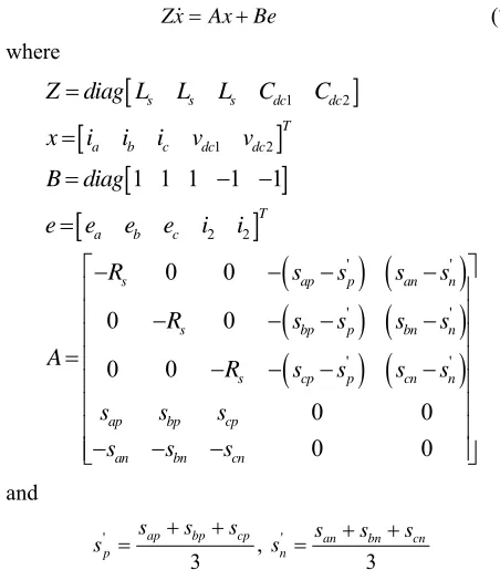
where
1 2 1 2 2 2 ' ' ' ' ' '1 1 1 1 1
0 0
0 0
0 0
0 0
0 0
s s s dc dc
T a b c dc dc
T a b c
s ap p
s bp p bn
s cp p cn n
ap bp cp an bn cn
Z diag L L L C C
x i i i v v
B diag
e e e e i i
an n n
R s s s s
R s s s s
A R s s s s
s s s
s s s
and ' , ' 3 3
ap bp cp an bn cn
p n
s s s s s s
s s
The physical meaning of the mathematical model in coordinates is pellucid, but variable parameters of ac reactors are unstable which is not suitable for the de-sign of control system, so the mathematical model in the rotating
abc
dq coordinates is:
' ' '
Z xA xB e (8)
where
' 1 2 1 2 '1 1 1 1
0 0
0 0
s s dc dc
T d q dc dc
T
d q L L
s s dp dn
s s qp qn
dp qp dn qn
Z diag L L C C
x i i v v
B diag
e e e i i
R L s s
L R s s
A s s s s
d-axis in the dq coordinates, it can be shown that: v e v e dc
d d s q s s d
q q s d s s q
L i L s R i
L i L s R i
(9)
where, s is the arithmetic operator of differential coeffi-cient.
Considering C 1Cdc2Cd, then
2dc dc
d dp dn d qp qn q L
dv v
s i s s i
dt R
C s
, ,
a b ec
d i * q v (10)
From the aforementioned model, the equivalent circuit of the three-level PWM rectifier in the coordi-nates can be obtained as shown in Figure 2.
dq
3. Control Strategy for the Three-level PWM
Rectifier Based on SVPWM
Similarly to the two-level PWM rectifier [26-34], the control target of the three-level PWM rectifier is to make the dc output voltage dc follow its reference value , while keeping the input currents ( ) approximately sinusoidal and in phase with the corresponding grid voltages ( ).
v v*dc
, ,
a b c
i i i
e e
Furthermore, to ensure the reliability of the system [35] the two special requirements of three-level PWM recti-fier: balance of neutral-point voltage and avoidance of excessive voltage jump in phase and line-to-line voltages must be satisfied.
Voltage oriented control (VOC) which is the classical and most popular control strategy for the three-level PWM rectifiers [32] provides excellent steady-state per-formance, acceptable dynamic performance and constant switching frequency for the rectifier compared with other strategies. The block diagram scheme of VOC strategy based on sliding mode control for the three level PWM rectifier is illustrated in Figure 3.
There are three control loops in the VOC strategy. The error between the reference dc-bus voltage and the sampled dc-bus voltage dc is processed by SMC, which produces the reference active current . As in the inner loops, -axis currents loop and -axis current loop use anti-windup IP controllers to make the actual currents and q) track their reference values ( and ). Generally, and in order to achieve near unity power factor condition, the controlled value of the q-axis current is set to zero.
* dc v * d i v q
(id
* d i * q i
Then, the errors are processed in two conventional anti-windup IP controllers to produce the output signals of * and , after coordinates transformation,
d
v v*
and *
v which can be obtained and used to produce
switching signals and c by three-level space vector pulse with modulation (SVPWM).
,
a Sb
S
,
a
e
S
As shown in Figure 3, in the three-level PWM grid
phase voltages ( eb), two grid phase currents (i i, )
and two dc-link voltages (vdc1,vdc2) are sampled.
3.1. Sliding Mode Control Design of the Output Voltage Loop
The main goal of the voltage control of the rectifier is keep the output voltage constant, ripple of the voltage small, and overshoot small and the regulation course short during transient conditions.
1 dc C L R d dpi s 2 dc C 1 dc V 2 dc V 2 C i 1 C i o i p i n i N P d dni s
sqpiq
q qni s q si L s R d e + d v s L + d i d si L s R q e + q v s
L iq
+
[image:3.595.309.533.197.352.2](a) (b)
Figure 2. Equivalent circuit of the three-level PWM recti-fier in d - q coordinates.
* dc v q i dc v 0 * q i a r * d i d i s L + abc SVPWM - Antiwindup IP a e b e SMC s L * v 1 dc V Three-level rectifier 2 dc V dq a i b i b c dq * v Antiwindup IP p i n i d e q e + - - + - + + + - - + + + - a
S Sb Sc
* d v * q v q i d i
[image:3.595.308.537.394.720.2]There are two external variables ( dc and iqfor the three-level PWM rectifier, where dc is determined by
v v
d
s , and iq is controlled by sq. Considering vdc and q as contestable output variables, standard state space can be obtained as
i 1 2 2 q s
d q dc
s s s
q
dc d d q q L
d
s R
i i v e
L L L
i d
v s i s i i
dt C q (11)
Substituting the error between reference and fact vari-able into “equation (10)”, then
1 1 1 q dc
iq vdc
y E x t z E s v e d e e dt
(12) where,
, ,
ref dc ref
iq iq q v dc dc
e i i e v v
and
ref
e
So, it can be concluded that selecting the two follow-ing slidfollow-ing surfaces, the stability and robustness of the system can be achieved:
1 eiq iq eiq qref q 0
s k e k i i (13)
2 1 dc 2 dc dc dc 0
v
v v
de de
s k e k e
dt dt
v
(14) By combining the above equations, then s2 can be
rewritten as
2 2 2d d q q
dc L
dc ref dc
d d
dc d
dc ref dc L q q d
d
s i s i
dv i
s v v
dt C C
dv C
v v i s i
dt C s
d i (15) In dq coordinates, d 3 RMS , , in the ideal sliding mode state,
e u eq0
q
s can be calculated and
sim-plified as
2 s d
q dc L i s v
(16)
Similarly, the output voltage dc will follow the ref-erence accurately, and based on the principle of power balance, v * dc v d
s is obtained as:
3
d s d RMS s d
d
dc dc
e R i u R i
s
v v
(17)
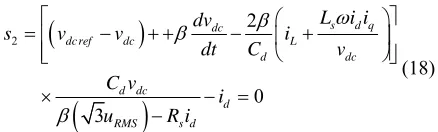
By substituting “equation (16)” and “equation (17)” into “equation (15)”, “equation (18)” can be deduced as
2 2 0 3s d q dc
dc ref dc L
d dc
d dc
d RMS s d
L i i dv
s v v i
dt C v
C v
i u R i
(18)
Therefore, sd and sq will not be relevant to the choice of sliding mode surface, and the sliding mode surface can be obtained as
1 eiq iq eiq qref q 0
s k e k i i (19)
2 dref d 0
s i i (20)
From “equation (18)” and “equation (20)”, the control rule for the outer voltage loop can be described as
2 3 dcd ref dc ref dc L
d d dc
RMS s d dv
i v v
dt C
C v
u R i
i (21)
The block scheme of the VOC strategy based on SMC for the three-level PWM rectifier is shown in Figure 3.
The error between reference dc-bus voltage and the sampled dc-bus voltage dc is processed by SMC, which produces the reference active current . and , (for unity power factor control, ) are compared with the measured grid current, d and q, respectively. Then, the errors are processed in two anti-windup IP controllers to produce the output signals of and , after coordinates transformation,
* dc v * d i * q v v * d i * q
i i*q0
i * v i * d v
and v* that can be obtained and used to produce switching signals a,
b and c by the three- level space vector pulse width modulation (SVPWM).
S
S S
3.2. Three-level Space Voltage Vector Modulation Algorithm
There are 27 output voltage vectors in the three-level VSI as shown in Figure 4. In Figure 5, suppose the desired
reference voltage vector lies in the triangle B which is in the first 60° sector (sector I).
Then, the function time of each output voltage vector should be calculated first as well as the corresponding time for the power devices to turn on or turn off.
The desired output voltage vector consists of 1 3 and 4 by the adjacent three vector compounding prin-ciple. Based on the volt-second balancing principle [36]:
, V V V
2 1 sin 3
2 sin 3 1
2 sin
a s
b s
c s
T T k
T T k
T kT (23)
[image:4.595.321.540.85.151.2]system sampling control cycle, Vref and is the am-plitude and angle of the reference voltage vector ref.
In the same way, the function time of the adjacent three-vectors could be fixed when it lies in the triangle A, C and D. The vector function time of the other five vec-tors could be deduced in a symmetrical manner.
V
According to the function time of each vector and the centro-symmetric vector sending sequence, the three phase output vectors sequential chart could be fixed when the reference vector ref lies in the triangle A, B, C and D in sector I, which also gets the space voltage vector modulation mode.
V
There are some similar SVPWM modes when the ref-erence vector lies in other vectors. According to the SVPWM mode and the function time of each vector cor-responding to each sector, the power devices driven sig-nal of the three phase arms could be obtained to control the three-level inverter in SVPWM mode.
PON
PNO ONN POO
N OPN NPN
OPO NON NPO
NPP OPP
NOO
NOP OOP
NNO
ONP NNP
PNN PPO
OON PP
POP ONO
[image:5.595.315.532.259.710.2]PNP
Figure 4. Space voltage vectors in three-level rectifier.
PON N
N ON
POO PPO
OON PPN
0
V
V
1PN
3
V
ref
V
b
T
a
T
a
T
b
T
c
T
2
V
4
V
5
V
c
T
AB C
D
[image:5.595.66.276.312.500.2]PPP OOO NNN
Figure 5. Synthesized reference vector in the first 60° sec-tor.
4. Simulation Results
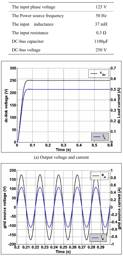
To validate the proposed control scheme proposed in this paper, a series of simulation tests have been conducted under Matlab/Simulink environment. The main parame-ters of the simulation system are given in Table 1.
Figure 6(a) shows the DC voltage and current
wave-forms where the DC output voltage reaches the given stable value (250 V) of the voltage in a short time. Fig-ure 6(b) shows the grid phase voltage (ea) and current (ia) waveforms. It can be seen that the grid current is in phase with the grid voltage, and the power factor is higher than 0.997.
Table 1. Rectifier parameter.
The input phase voltage 125 V
The Power source frequency 50 Hz
The input inductance 37 mH
The input resistance 0,3 Ω
DC-bus capacitor 1100μF
DC-bus voltage 250 V
(a) Output voltage and current
(b) Grid source side voltage and current
[image:5.595.65.276.527.707.2]Figure 7 shows the simulation results when the load
changes from 500 Ω to 750 Ω at t = 0.4 s. Figure 7(a)
shows the output DC voltage and current waveforms when the load and input voltage fluctuates, the system can adjust to the desired value of the voltage in a short period of time. Figure 7(b) shows the waveforms of the
grid source side current, the current always maintains unity power factor in the dynamic process.
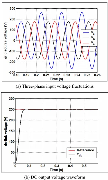
Moreover, in view of the actual operating conditions, there are more or less fluctuations of the three-phase in-put voltage especially three-phase inin-put voltage unbal-ance in the operation of the circumstunbal-ances. Figure 8(a)
shows unbalanced three-phase input voltage in the sys-tem, single-phase unbalance is up to 20%, DC output voltage fluctuations is less than 0.2 V as shown in Figure 8(b).
To validate the superiority of SMC over conventional PI controller, comparative simulations are conducted and the results are shown in Figure 9. Figure 9(a) shows the
waveform of the dc-bus voltage under conventional PI controller while Figure 9(b) is that of SMC. It can be
seen clearly that the overshoots of the dc-bus voltage for the rectifier with PI controller is much higher than that with SMC, and the dynamic performance of the system is improved significantly.
(a) Output voltage and current
[image:6.595.331.513.416.719.2](b) Grid source side current
Figure 7. Simulation waveforms at load changes.
(a) Three-phase input voltage fluctuations
(b) DC output voltage waveform
Figure 8. Voltage unbalance at the DC output waveforms.
(a) dc-bus voltage with conventional PI
(b) dc-bus voltage with SMC
5. Conclusions
The problem of the voltage control system of the three- level rectifier is thoroughly analyzed and presented in this paper. Through the study on the voltage equation of the rectifier, the nonlinear characteristic of the voltage control is carefully discussed and detailed based on a new strategy which uses sliding mode control (SMC). The proposed control strategy is adopted for the dc bus voltage control to obtain better dynamic performance based on the presented mathematical model. Simulation results which are included in this paper, indicate that the unity power factor is achieved and the proposed scheme exhibits better dynamic and steady state performance than conventional controller.
6. Acknowledgements
The author would like to express his deep gratitude to the President of the University of Hail, in Saudi Arabia for his continuous moral support and encouragement to re-searchers as well as for financial support for undertaking this research work.
REFERENCES
[1] J. R. Rodigues, J. W. Dixon, J. R. Espinoza, J. Pontt and P. Lezana, “PWM Regenerative Rectifiers: State of Art,”
IEEE Transactions on Industrial Electronics, Vol. 52, No.
1, 2005, pp. 5-22. doi:10.1109/TIE.2004.841149
[2] M. Liserre, R. Teodorescu and F. Blaabjerg, “Multiple Harmonics Control for Three-Phase Grid Converter Sys-tems with the Use of PI-RES Current Controller in a Ro-tating Frame,” IEEE Transactions on Power Electronics,
Vol. 21, No. 3, 2006, pp. 836-841.
doi:10.1109/TPEL.2006.875566
[3] V. Blasko and V. Kaura, “A New Mathematical Model and Control of a Three-Phase AC-DC Voltage Source Converter,” IEEE Transactions on Power Electronics,
Vol. 12, No. 1, 1997, pp. 116-123.doi:10.1109/63.554176
[4] H. Komurcugil and O. Kukrer, “Lyapunov-Based Control for Three-Phase PWM AC/DC Voltage-Source Convert-ers,” IEEE Transactions on Power Electronics, Vol. 13,
No. 5, 1998, pp. 801 - 813. doi:10.1109/63.712278
[5] T. S. Lee, “Input-Output Linearization and Zero-Dynamics Control of Three-Phase AC/DC Volt-age-Source Converters,” IEEE Transactions on Power Electronics, Vol. 18, No. 1, 2003, pp. 11-22.
doi:10.1109/TPEL.2002.807145
[6] D. C. Lee, G. M. Lee and K. D. Lee, “DC-Bus Voltage Control of Three-Phase AC/DC PWM Converters Using Feedback Linearization,” IEEE Transactions on Industry Applications, Vol. 36, No. 3,2000, pp. 826-833.
doi:10.1109/28.845058
[7] Y. Ye., M. Kazerani and V. H. Quintana, “Modeling, Control and Implementation of Three-Phase PWM Con-verters,” IEEE Transactions on Power Electronics, Vol.
18, No. 3, pp. 857-864, 2003.
[8] H. C. Mao, D. Boroyevich and C. Y. Lee, “Novel Re-duced-Order Small-Signal Model of Three-Phase PWM Rectifier and Its Application in Control Design and Sys-tem Analysis,” IEEE Transactions on Power Electronics, Vol. 13, No. 3, 1998, pp. 511-521.
[9] S. Chattopadhyay and V. Ramanarayanan, “Digital Im-plementation of a Line Current Shaping Algorithm for Three Phase High Power Factor Boost Rectifier without Input Voltage Sensing,” IEEE Transactions on Power Electronics, Vol. 19, No. 3, 2004, pp. 709-721.
[10] T. T. Jin and K. M. Smedley, “A Universal Vector Con-troller for Four-Quadrant Three-Phase Power Convert-ers,” IEEE Transactions on Circuits and Systems Part I: Fundamental Theory and Applications, Vol. 54, No. 2, 2007, pp. 377-390.
[11] J. W. Kolar, H. Ertl, L. Edelmoser and F. C. Zach, “Analysis of the Control Behavior of a Bidirectional Three-Phase PWM Rectifier System,” in Proc. Eur. Conf. Power Electron. Appl. 1991, pp. 2095-2100.
[12] S. Hiti and D. Boroyevich, “Control of Front-End Three-Phase Boost Rectifier,” IEEE Appl. Power Elec-tron. Conf. Expo., Vol. 2, 1994, pp. 927-933.
[13] S. Hiti and D. Boroyevich and C. Cuadros, “Small-Signal Modeling and Control of Three-Phase PWM Convert-ers,"”in Proc. Appl. Soc. Annu. Meeting. Vol. 2, 1994, pp. 1143-1150.
[14] D. Graovac and V. Katic, “A Method of PWM Rectifier Control in Voltage Linked AC/DC/AC Converter,” in Proc. 9th Mediterranean Electrotech. Conf. (MELECON 1998), Vol. 2, 1998, pp. 1032-1036.
[15] J. Clerk Maxwell, “A Treatise on Electricity and Magnet-ism,” 3rd ed, Oxford, Vol. 2, 1892, pp. 68-73.
[16] I. S. Jacobs and C. P. Bean, “Fine Particles, Thin Film and Exchange Anisotropy,” in Magnetism, G.T. Rado and H. Suhl, Eds. New York: Academic, Vol. 3, 1963, pp. 271-350.
[17] G. Eason, B. Noble and I.N. Sneddon, “On Certain Inte-grals of Lipschitz-Handkel Type Involving Products of Bessel Functions,” Phil. Trans. Roy. Soc. London, Vol. A247, 1955, pp. 529-551.
[18] K. S. Walgama, S. Ronnback and J. Sternby, “Generali-zation of Conditioning Technique for Anti-Windup Com-pensators,” Proc. Inst. Elect. Eng. Vol. 139 D, No. 2,
1992, pp. 109-118.
[19] M. V. Kothare, P. J. Campo, M. Morari and C. N. Nett, “A Unified Frame Work for the Study of Anti-Windup Designs,” Automatica, Vol. 30, No. 12, 1994, pp.
1863-1869.doi:10.1016/0005-1098(94)90048-5
[20] Y. Ping, D. Vrancic and R. Hanus, “Anti-Windup, Bump less, and Conditioned Transfer Techniques for PID Con-trollers,” IEEE Trans. Contr. Syst. Technol. Vol. 16, 1996,
pp. 48-57.doi:10.1109/37.526915
[21] K. Hartani, M. Bourahla, Y. Miloud and M. Sekour, “Electronic Differential with Direct Torque Fuzzy Con-trol for Vehicle Propulsion System,” Turkish Journal of Electrical Engineering & Computer Sciences, Vol. 17,
No. 1, 2009, pp. 21-38.
“Performance Evaluation of Three Control Strategies for Three-Level Neutral Point Clamped PWM Rectifier,” in Proc. IEEE APEC’08, 2008, pp. 259-264.
[23] T. Lu, Z. M. Zhao, L. O. Yuan and S. P. Wang, “Instan-taneous Energy Balacing in Three-Level Neutral Point Clamped Converters,” in Proc. IEEE VPPC’08, Harbin,
China, 2008, p. 288.
[24] Y. C. Zhang, Z. M. Zhao, L. Q. Yuan, T. Lu and T. CH. Zhang, “Direct Power Control for Three-Level PWM Rectifier,” Transactions of china Electro technical Soci-ety, Vol. 23, No. 5, 2008, pp. 62-68.
[25] B. Yin, R. Oruganti, S. K. Panda, Ashoka and K. S. Bhat, “A Simple Single-Input-Single-Output (SISO) Model for a Three-Phase PWM Rectifier,” IEEE Trans. Power Elec-tron. Vol. 24, No. 3, 2009, pp. 620-631.
[26] B. Singh, B. N. Singh, A. Chandra, K. All-Haddad, A. Pandey and D. P. Kothari, “A Review of Three-Phase Improved Power Quality Ac-Dc Converters,” IEEE Transactions on Industrial Electronics,Vol. 51, No. 3,
2004, pp. 641-660.doi:10.1109/TIE.2004.825341
[27] Y. Sud and T. A. Lipo, “Modeling and Analysis of In-stantaneous Power Flow for Three-Phase Boost Rectifier under Generalize Unbalanced Network,” IEEE Transac-tions on Power Electronics, Vol. 21, No. 3, 2006, pp.
1530-1540.
[28] X. H. Wu, S. K. Panda and J. X. Xu, “Analysis of the Instantaneous Power Flow for Three-Phase Boost Recti-fier under Unbalanced Supply Voltage Conditions,” IEEE Transactions on Power Electronics, Vol. 23, No. 4, 2008,
pp. 1679-1691.doi:10.1109/TPEL.2008.925158
[29] X. H. Wu, S. K. Panda and J. X. Xu, “Dc Link Voltage and Supply-Side Current Harmonics Minimization of Three-Phase PWM Boost Rectifier Using Frequency Domain Based Repetitive Current Controllers,” IEEE
Transactions on Power Electronics, Vol. 23, No. 4, 2008,
pp. 1987-1997.doi:10.1109/TPEL.2008.925428
[30] B. Yin, R. Oruganti, S. K. Panda and A. K. S. Bhat, “An Output-Power-Control Strategy for a Three-Phase PWM Rectifier under Unbalanced Supply Conditions,” IEEE Trans. Ind. Electron. Vol. 55, No. 5, 2008, pp.
2140-2151.
[31] D. Roiu, R. Bojoi, L. R. Limongi and A. Tenconi, “New Stationary Frame Control Scheme for Three Phase PWM Rectifier under Unbalanced Voltage Dips Conditions ,” in Proc. IEEE, 2008, pp. 1-7.
[32] I. E. otadui, U. Viscarret, M. Caballero, A. Rufer and S. Bacha, “New Optimized PWM VSC Control Structures and Strategies under Unbalanced Voltage Transients,”
IEEE Transactions on Industrial Electronics, Vol. 54, No.
5, 2007, pp. 2902-2914.doi:10.1109/TIE.2007.901373
[33] A. Vladan Stankovic, and K. Chen, “A New Control Method for Input-Output Harmonic Elimination of the PWM Boost Rectifier under Extreme Unbalanced Oper-ating Conditions,” IEEE Transactions on Industrial Elec-tronics, Vol. 56, No. 7, 2009, pp. 2420-2430.
doi:10.1109/TIE.2009.2017550
[34] Z. Li, Y. Li, P. Wang, H. Zhu, C. Liu and F. Gao, “Sin-gle-Loop Digital Control of High-Power 400Hz Ground Power Unity for Airplanes,” IEEE Transactions on In-dustrial Electronics, Vol. 57, No. 2, 2010, pp. 532-543.
doi:10.1109/TIE.2009.2033490
[35] T. Lu, Z. M. Zhao, Y. C. Zhang, Y. CH. Zhang, and L. Q. yuan, “A Novel Direct Power Control Strategy for Three-Level PWM Rectifier Based on Fixed Synthesizing Vectors,” in Proc. ICEM’08, Wuhan, China, 2008, p.
520.