2017 3rd International Conference on Electronic Information Technology and Intellectualization (ICEITI 2017) ISBN: 978-1-60595-512-4
A Sampling Holder Using A
Bootstrapped Switch
Yue Ma
ABSTRACT
This paper describes the design of a sampling holder, Using a higher linearity bootstrapped switch, by using the bottom plate sampling to offset the effect of charge injection effect, By using the capacitance flip type structure to reduce power consumption, designing a high gain and high speed operational trans-conductance amplifier to improve gain and speed.
INTRODUCTION
Sample and hold circuit is composed of analogy switch, storage element and a buffer amplifier. It is located in front of the analogy to digital converter. Comparing with the post stage circuit, the input signal changes are much larger in the amplitude and frequency. So the linear sample and hold circuit level is high. In order to improve the linearity of the sample holder and meet the requirements of high precision, this paper describes the design of a sampling holder.
THE DESIGN OF BOOTSTRAPPED SWITCH
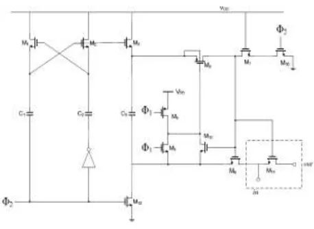
Poor linearity of ordinary switch is not suitable for large signal and high precision application. The bootstrapped switch is often used in the high precision analog-to-digital conversion. Figure 1 shows the circuit structure of the classical bootstrapped switch.
_______________________
Figure 1. The structure of bootstrapped switch.
In figure 1, the M11 is the core of the switch for the transmission of the input signal; all the rest are auxiliary switch. 1 and 2 is a two-phase non-overlapping clock. M3 and M12 and capacitor C3 form a charging circuit. They will charge C3 to voltage on VDD. This makes the gate -source voltage of M11 to maintain in this constant value at turn-on state. The role of the cross coupling M1, M2 and C1, C2 on the left is to constitute a voltage multiplier circuit, and improve the voltage of the gate terminal of M3 to make C3 fully charged. The role of M8 and M9 is to partition and conducting the loop made by C3 in M11 pipe gate source end. The M4, M5 and M10 control them through. M7 and M13 according to the M10 and M8 play a protective role. The value of C3 must be large enough to avoid charge leaked M11 gate end parasitic capacitance.
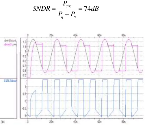
Figure 2 shows the simulation results. The first line of the waveform is sine input signal and output signal. It can be seen that the output accurately track live input. Second waveform is the voltage differential between sampling switch gate terminal and the input terminal. The values in the conduction stage maintain a constant value to meet the purpose to increase the switch linearity.
THE SELECT OF THE SAMPLING CAPACITOR
The sampling capacitor is selected according to the requirement of noise and signal to noise ratio. The sampling holder noise is mainly composed of sampling phase switch thermal noise and keep stage operational amplifier thermal noise. By the derivation of estimation, we can the output equivalent noise of sampling holder.
2 2
, , ,
1 4 1
2 2
3
B r B r
n TH n track n hold
s Leff
k T k T P
C C
(1)
[image:2.612.182.411.81.248.2]74
sig
q n
P
SNDR dB
P P
[image:3.612.172.423.88.304.2](2)
Figure 2. The bootstrapped switch waveform simulation.
In the formula, Psig is the signal power, and Pq is quantization noise power, and Pn
is the total noise power. Setting up quantization noise power and total noise powerare equal, it can estimate the size of the sampling capacitor.
THE DESIGN OF OPERATIONAL AMPLIFIER
Operational amplifier is the key module in sampling holder. In order to realize the sampling holder with high speed and high precision, we need to design the operational amplifier with high DC gain, high bandwidth, and high swing. When designing,we should estimate operational amplifier index according to the sampling holder index to select the structure of the operational amplifier. Then we can choose parameters of each MOS according to the index value of amplifier, and adjust through simulationresult. Because the circuit is fully differential structure, the design of the common mode feedback circuit is essential.
Determine The DC Gain
Finite DC gain will produce static error. According to the static error allowed we can calculate the DC gain of the operational amplifier. With static error sampling holder for 1/4LSB, we can get static
1 1
4
static LSB
A
Then we can get 2 1 2 1 4 N A LSB
(4)
The N=12 substitution can be
84
A dB
Determine The Unit Gain Bandwidth
The unity-gain bandwidth has something to do with establishing linear time and dynamic error. The total setup timeconsists of the establishment of large signal time and establish linear time. It relates to the distribution of two stage setup time. We can estimate the proportion of the two establish times.
, , ln 2 L eff dynamic REF ov tail L eff C gm n V V I C
(5)
The corresponding values are substituted into Equation (5), then we can get n=4. The establishment of the total time is about half a clock cycle. Removing the non- overlap time and clock edge, the effective establishtime is about 4.6ns. So the linear establish time is 3.7ns, and slew time is 0.9ns. The loop unit gain bandwidth.
ln 1 dynamic linear GBW t
(6)
If
1 4
dynamic LSB
(7)
Then
431
GBW MHz
(8)
Other Indicators
In order to establish the accuracy in a given time, we should also meet the requirements of the phase margin, in addition to meet the DC gain, gain bandwidth product outside unit. The phase margin has been explained in the front. In order to meet faster set goals, we should make the phase margin at around 72 degrees. In addition, the operational amplifier should also meet the input differential swing and output one to the requirements of 1.5V in the power supply voltage of 1.8V.
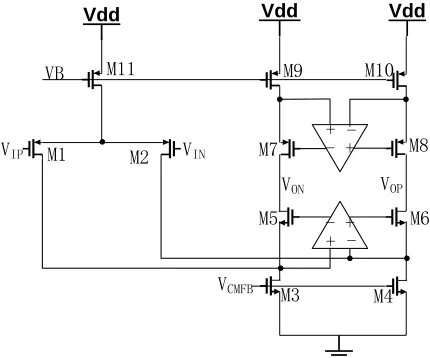
[image:5.612.176.391.258.437.2]According to the design index, we use a folded cascade gain bootstrap operational amplifier with the bigger input common mode range and high gain. Figure 3 shows the circuit diagram.
Vdd Vdd Vdd
VB
VCMFB
VIP VIN
VON VOP
M1 M2
M3 M4
M5 M6
M7 M8
M9 M10
M11
+ -- + + -- +
Figure 3. The folded cascade gain bootstrap operational amplifier.
THE SIMULATION OF OPERATIONAL AMPLIFIER
Design And Simulation of Main Operational
The main operational amplifier is the classic folded cascade structure, a PMOS tube is used as input, and witch has less 1/f noise. Using PMOS tube as input to the tube has another advantage is that substrate P transistor N that is well and the source end can be connected together amplifier. This structure can remove the back gate effect, and also has good symmetry. In addition, the current source in the folding point uses N tube to reduce parasitic capacitance. This design can achieve higher speed.
input grid length should be for the minimum length of tube. In order to achieve higher gain, other transistor should take larger gate length. As current source, the MOS tube should take larger gate length to improve the accuracy of the current mirror and common mode rejection ratio. For input tube, should be properly decreasing the driving voltage in order to achieve greater efficient of trans conductance. With low current gain greater trans conductance, namely greater unity gain bandwidth product. In addition, the tube the input of the trans conductance after also can inhibit the noise level. For the current pipe and common source common grid. Too much trans conductance can introduce more noise, so we should take larger driving voltage. The larger driving voltage can make the matching degree of the current source pipe to be better. But the larger driving voltage will decrease voltage swing.
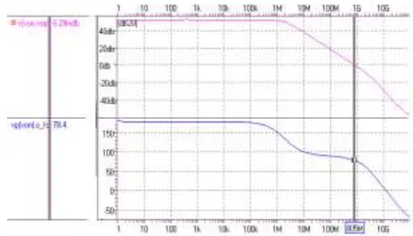
Figure 4. The main op-amp frequency characteristic.
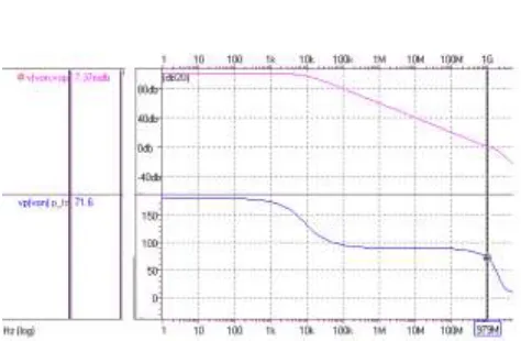
According to the above design idea, we designed the main operational amplifier. Small signal analysis of the operation amplifier, amplitude frequency and phase frequency response waveform, as show in figure 4. For two curves in a diagram the amplitude frequency and phase frequency response waveform. We can see by the simulation results of main operational unit gain bandwidth is 805MHz, and the DC gain is 52.7 dB, and the phase margin is 78°.
Design of Auxiliary Operational Amplifier
The too low gain of op-amp cannot satisfy the static error, so we use auxiliary op-amp gain. Auxiliary op-amp adopts fold same source grid structure, and according to input level of discretion to choose the type of input on the tube. In the fold point potential is low, so choose P type tube. Similarly, another should choose N type tube.
capacitance of auxiliary op-amp. When circuit design should ensure that the phase margin of auxiliary operational amplifier is large enough. The access of auxiliary operational amplifier also introduces a zero-pole extremely, located in the auxiliary op-amp unit gain bandwidth. A zero-pole is in the step response corresponding index of items. If the pole zero smaller, can slow down the whole movement of the step response. Therefore, the design should be the design of large enough. At the same time, we also should not be more than the main operational time poles caused by stability problems. The result can be expressed as the following formula.
, , 2,
u main u boost p main
[image:7.612.178.415.232.387.2]
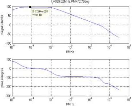
(9)Figure 5. The overall op-amp frequency characteristic.
In the formula, ωu,main is the unit gain bandwidth of primary op-amp, and ωu,boost is
the unit gain bandwidth of auxiliary amp, and is the second pole of primary op-amp, and β is the feedback coefficient.
The Overall Operational Simulation
The Loop Simulation
The op-amp is applied to closed loop circuit. In order to ensure the stability of the closed loop circuit, it is necessary in the loop simulation.
Differential Looptest
+
-- + Vip
Vim
Vom
Vop
XP
XM CSP
CSM
CLM
CLP
Vbp
Vbm
OTA R1
[image:8.612.175.406.155.257.2]R2
Figure 6a.The simulation circuit of loop circuit of sampling keeping circuit.
Figure 6b. The loop frequency characteristic simulation result.
The simulation circuit is shown in figure 6, and the simulation analysis is based on a Middle Brook loop analysis method. The resistance in the graph is to offer in the simulation to the op-amp common-mode input level.
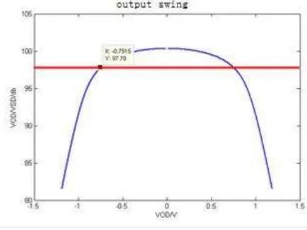
The Simulation of Output Swing
[image:8.612.185.414.296.480.2]the amplifier gain is greater than 97.7dB, when the output swing is between -750mV and 750mV. The result meet the requirement of static error.
Figure 7. The output swing simulation result.
The Common-mode Feedback Circuit Design
Compared with the single side structure, fully differential structure has larger output swing and ability to resist noise and common mode rejection ratio. However the difference structure of the op-amp offset can not achieve self-sufficiency, and its output current depends on the two current source located in circuit above and below. When the current provided by above two current source is not completely equal, the output voltage will be significantly deviate from the set of common mode level. In order to solve this problem, we must use the common-mode feedback circuit to dynamically measure the common-mode output level. To the one of the current source to do corresponding adjustment, so as to stabilize the main output common-mode level.
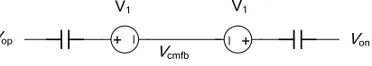
One Switched capacitor common mode feedback circuit is shown in figure8. The following briefly describes its working principle. The role of the capacitance C1,C4 is continuously update voltage difference on both ends, then recharge the capacitor C2,C3. As shown in figure 9, in the case that the charge is updated at the ends of the capacitor voltage V1, then V1=Vcm-Vbias. So we can get,
( )
cmfb op cm bias
V V V V (10)
( )
cmfb on cm bias
Vcm
Vbias
Vcm
Vbias
Vcmfb
Vop Von K1
K2
K3
K4
K5
K6
K7
K8
[image:10.612.184.418.87.143.2]C1 C2 C3 C4
Figure 8. Switched capacitor common mode feedback circuit.
+ +
V1 V1
Vcmfb
Vop Von
Figure 9. The equivalent circuit of switched capacitor common mode feedback circuit.
Two formula combined divided by two is
( )
2
op on
cm cmfb bias
V V
V V V
(12)
As seen in formula (12), if Vcmfb and Vbias isequal, the output common-mode level
is equal to Vcm.
The Sample Holder Dynamic Performance Simulation
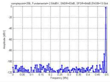
Taking transient analysis to the sample holder, and taking fast Fourier transform to sample point, we can obtain dynamic characteristics of the sample holder. In the simulation, in order to avoid the spectrum leakage and same sampling point in one cycle, the relation between input signal frequency and sampling signal frequency should meet the follow formula.
in
clk
f M
f N (13)
In the formula, fin and fclk is the input signal frequency and sampling signal frequency respectively, and N is the number of sampling points, and M is the signal cycle number. N and M are integers, and they are prime Numbers.
[image:10.612.194.400.200.237.2]Figure 10. Dynamic characteristics of sample holder.
CONCLUSIONS
The key module of flow line structure in ADC is analyzed. Each module and the whole circuit design and simulation results are given. At the end of the double sampling technique is studied, the improvement of circuit design, and the corresponding simulation results are given.
REFERENCES
1. Abo A. Design for reliability of low-voltage, switched-capacitor circuits [D], UC Berkeley, 1999.
2. Cho T. Low-power, Low-voltage analog-to-digital conversion techniques using pipelined
Architecture[D]. Berkeley: University of California, 1995.
3. Kamath B.Y.T & R.G. Meyer. Relationship between frequency response and settling time of
operational amplifiers [J], IEEE Journal of Solid-State Circuits, 1974, 9(6): 347-352.
4. Bult K.& J.G. Geelen. A fast-settling CMOS op amp for SC circuits with 90-dB DC gain [J],
IEEE Journal of Solid-State Circuits, 1990,25(6): 1379-1384.
5. Choksi O. & L. R. Carley. Analysis of Switched-Capacitor Common-Mode Feedback Circuit [J].