International Journal of Emerging Technology and Advanced Engineering
Website: www.ijetae.com (ISSN 2250-2459,ISO 9001:2008 Certified Journal, Volume 3, Issue 3, March 2013)
417
A Review on Reversible Logic Gates and their Implementation
Raghava Garipelly
1, P.Madhu Kiran
2, A.Santhosh Kumar
31, 2, 3 Assistant Professor, Dept of ECE, SCCE, Karimnagar, INDIA
Abstract—Reversible logic is one of the most vital issue at present time and it has different areas for its application, those are low power CMOS, quantum computing, nanotechnology, cryptography, optical computing, DNA computing, digital signal processing (DSP), quantum dot cellular automata, communication, computer graphics. It is not possible to realize quantum computing without implementation of reversible logic. The main purposes of designing reversible logic are to decrease quantum cost, depth of the circuits and the number of garbage outputs. This paper provides the basic reversible logic gates, which in designing of more complex system having reversible circuits as a primitive component and which can execute more complicated operations using quantum computers. The reversible circuits form the basic building block of quantum computers as all quantum operations are reversible. This paper presents the data relating to the primitive reversible gates which are available in literature and helps researches in designing higher complex computing circuits using reversible gates.
Keywords— Reversible logic, Reversible gate, Power dissipation, Garbage, Quantum cost, Quantum-dot Cellular Automata, Reversible Computing.
I. INTRODUCTION
Energy dissipation is one of the major issues in present day technology. Energy dissipation due to information loss in high technology circuits and systems constructed using irreversible hardware was demonstrated by R. Landauer in the year 1960. According to Landauer’s principle, the loss of one bit of information lost, will dissipate kT*ln (2) joules of energy where, k is the Boltzmann’s constant and k=1.38x10 -23 J/K, T is the absolute temperature in Kelvin[1]. The primitive combinational logic circuits dissipate heat energy for every bit of information that is lost during the operation. This is because according to second law of thermodynamics, information once lost cannot be recovered by any methods.
In 1973, Bennett, showed that in order to avoid kTln2 joules of energy dissipation in a circuit it must be built from reversible circuits [2].
According to Moore’s law the numbers of transistors will double every 18 months. Thus energy conservative devices are the need of the day. The amount of energy dissipated in a system bears a direct relationship to the number of bits erased during computation. Reversible circuits are those circuits that do not lose information.
The most prominent application of reversible logic lies in quantum computers [3]. A quantum computer will be viewed as a quantum network (or a family of quantum networks) composed of quantum logic gates; It has applications in various research areas such as Low Power CMOS design, quantum computing, nanotechnology and DNA computing.
Quantum networks composed of quantum logic gates; each gate performing an elementary unitary operation on one, two or more two–state quantum systems called qubits. Each qubit represents an elementary unit of information; corresponding to the classical bit values 0 and 1. Any unitary operation is reversible and hence quantum networks effecting elementary arithmetic operations such as addition, multiplication and exponentiation cannot be directly deduced from their classical Boolean counterparts (classical logic gates such as AND or OR are clearly irreversible).Thus, quantum arithmetic must be built from reversible logical components [3]. Reversible computation in a system can be performed only when the system comprises of reversible gates. A circuit/gate is said to be reversible if the input vector can be uniquely recovered from the output vector and there is a one-to-one correspondence between its input and output assignments [4-6].
An N*N reversible gate can be represented as
Iv=(I1,I2,I3,I4,………IN) Ov=(O1,O2,O3,……….ON).
Where Iv and Ov represent the input and output vectors respectively.
In quantum computing, by considering the need of reversible gates, a literature survey has been done and the mostly available reversible logic gates are presented in this paper.
II. BASIC DEFINITIONS PERTAINING TO REVERSIBLE LOGIC
A.
Reversible Function:
The multiple output Boolean function F(x1; x2; :::; xn) of n Boolean variables is called reversible if:
a. The number of outputs is equal to the number of inputs;
International Journal of Emerging Technology and Advanced Engineering
Website: www.ijetae.com (ISSN 2250-2459,ISO 9001:2008 Certified Journal, Volume 3, Issue 3, March 2013)
418
In other words, reversible functions are those that perform permutations of the set of input vectors[7].
B.
Reversible logic gate:
Reversible Gates are circuits in which number of outputs is equal to the number of inputs and there is a one to one correspondence between the vector of inputs and outputs[8-10]. It not only helps us to determine the outputs from the inputs but also helps us to uniquely recover the inputs from the outputs.
C.
Ancilla inputs/ constant inputs:
This refers to the number of inputs that are to be maintain constant at either 0 or 1 in order to synthesize the given logical function[11].
D.
Garbage outputs:
Additional inputs or outputs can be added so as to make the number of inputs and outputs equal whenever necessary. This also refers to the number of outputs which are not used in the synthesis of a given function. In certain cases these become mandatory to achieve reversibility. Garbage is the number of outputs added to make an n-input k-output function ((n; k) function) reversible.
We use the words ―constant inputs‖ to denote the present value inputs that were added to an (n; k) function to make it reversible. The following simple formula shows the relation between the number of garbage outputs and constant inputs .
Input + constant input = output + garbage. [7]
E.Quantum cost:
Quantum cost refers to the cost of the circuit in terms of the cost of a primitive gate. It is calculated knowing the number of primitive reversible logic gates (1*1 or 2*2) required to realize the circuit. The quantum cost of a circuit is the minimum number of 2*2 unitary gates to represent the circuit keeping the output unchanged. The quantum cost of a 1*1 gate is 0 and that of any 2*2 gate is the same, which is 1 [12].
F.Flexibility :
Flexibility refers to the universality of a reversible logic gate in realizing more functions[13].
G.Gate Level :
This refers to the number of levels in the circuit which are required to realize the given logic functions.
H. Hardware Complexity :
This refers to the total number of logic operation in a circuit. Means the total number of AND, OR and EXOR operation in a circuit [14] and [15].
I. Design Constraints for Reversible Logic Circuits:
The following are the important design constraints for reversible logic circuits.
Reversible logic gates do not allow fan-outs.
Reversible logic circuits should have minimum
quantum cost.
The design can be optimized so as to produce
minimum number of garbage outputs.
The reversible logic circuits must use minimum
number of constant inputs.
The reversible logic circuits must use a minimum logic depth or gate levels
III. REVERSIBLE LOGIC GATES
There are many number of reversible logic gates that exist at present. The quantum cost of each reversible logic gate is an important optimization parameter [16]. The quantum cost of a 1x1 reversible gate is assumed to be zero while the quantum cost of a 2x2 reversible logic gate is taken as unity. The quantum cost of other reversible gates is calculated by counting the number of V, V+ and CNOT gates present in their circuit. V is the square root of NOT gate and V+ is its Hermitian. The V and V+ quantum gates have the following properties:
V * V = NOT ………. (1) V * V+ = V+ * V = 1 ………. (2) V+ * V+ = NOT ………. (3)
Some of the important reversible logic gates are,
1)NOT Gate
The simplest Reversible gate is NOT gate and is a 1*1 gate[7]. The Reversible 1*1 gate is NOT Gate with zero Quantum Cost is as shown in the Figure 1.
(a) Block diagram (b) symbol
Figure1. NOT gate
2)CNOT GATE
CNOT gate is also known as controlled-not gate. It is a 2*2 reversible gate. The CNOT gate can be described as:
P=A’
International Journal of Emerging Technology and Advanced Engineering
Website: www.ijetae.com (ISSN 2250-2459,ISO 9001:2008 Certified Journal, Volume 3, Issue 3, March 2013)
419
Iv = (A, B) ; Ov = (P= A, Q= A B)
Iv and Ov are input and output vectors respectively. Quantum cost of CNOT gate is 1[17]. Figure 2 shows a 2*2 CNOT gate and its symbol.
(a) Block diagram (b) symbol
Figure 2: CNOT Gate
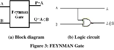
3)FEYNMAN Gate
The Feynman gate which is a 2*2 gate and is also called as Controlled NOT and it is widely used for fan-out purposes. The inputs (A, B) and outputs P=A, Q= A XOR B. It has Quantum cost one[19].
[image:3.612.339.538.180.262.2](a) Block diagram (b) Logic circuit
Figure 3: FEYNMAN Gate
4)Double Feynman Gate (F2G)
[image:3.612.70.266.325.412.2]It is a 3*3 Double Feynman gate [20].The input vector is I (A, B, C) and the output vector is O (P, Q, R). The outputs are defined by P = A, Q=AÅB, R=AÅC. Quantum cost of Double Feynman gate is 2.
Figure 4: Double Feynman gate.
5)TOFFOLI Gate:
TOFFOLI gate which is a 3*3 gate with inputs (A, B, C) and outputs P=A,Q=B, R=AB XOR C. It has Quantum cost five[21].
(a) Block diagram (b) Logic circuit
Figure 5: Toffoli Gate
6)FREDKIN Gate:
Fredkin gate which is a 3*3 gate with inputs (A, B, C) and outputs P=A, Q=A'B+AC, R=AB+A'C. It has Quantum cost five[22].
(a) Block diagram (b) Logic circuit
Figure 6: Fredkin Gate
7)PERES Gate:
Peres gate which is a 3*3 gate having inputs (A, B, C) and outputs P = A; Q = A XOR B; R = AB XOR C. It has Quantum cost four[23].
[image:3.612.345.533.334.410.2](a) Block diagram (b) Logic circuit
Figure 7: Peres Gate
8)TR Gate :
It is a 3x3 gate and its logic circuit and its quantum implementation is as shown in the figure. It has quantum cost six [24].
[image:3.612.334.554.484.552.2]
(a) Block diagram (b) symbol
Figure 8: TR Gate
9)NG Gate :
It is a 3x3 gate and its logic circuit and its quantum implementation is as shown in the figure [25].
[image:3.612.81.259.485.547.2](a) Block diagram (b) symbol
[image:3.612.73.267.618.691.2]International Journal of Emerging Technology and Advanced Engineering
Website: www.ijetae.com (ISSN 2250-2459,ISO 9001:2008 Certified Journal, Volume 3, Issue 3, March 2013)
420
10) R Gate:
[image:4.612.327.556.177.393.2]It is a 3x3 gate and its logic circuit is as shown in the figure. The gate can be used to invert a signal and also to duplicate a signal [26]. Quantum implementation of R gate is not discussed by author.
Figure 10: R Gate Block diagram
11) URG Gate:
[image:4.612.113.220.187.240.2]It is a 3*3 gate with inputs (A, B, C) and outputs P= (A+B) xor C, Q= B, R = AB xor C [27]. Quantum implementation of R gate is not discussed by author.
Figure 11: URG Gate Block diagram
12) BJN Gate:
It is a 3x3 gate and its logic circuit and its quantum implementation is as shown in the figure. It has quantum cost five [24].
[image:4.612.115.221.318.373.2]
(a) Block diagram (b) Logic circuit
Figure 12: BJN Gate
13) MCL gate:
[image:4.612.343.532.453.524.2]The MCL gate is a 3x3 gate which maps the inputs A, B, C to P= (B+C)’, Q= (A+B)’, R=A [24].
Figure 13: MCL Gate Block diagram
14) NFT Gate:
It is a 3x3 gate and its logic circuit and its quantum implementation is as shown in the figure. It has quantum cost five [24].
a) Block diagram
(b) Logic circuit
Figure 14: BJN Gate
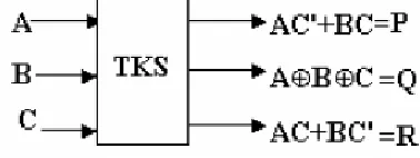
15) TKS Gate:
[image:4.612.66.271.458.532.2]The TKS gate can be used to implement any Boolean function since two of its outputs (P & R) can function as 2:1 multiplexer [28].
Figure 15: TKS Gate Block diagram
16) TSG Gate:
The TSG gate is a (4, 4) reversible gate. The most significant aspect of this gate is that it can work singly as a reversible full adder, that is, a reversible full adder can be implemented using a single gate only [29].
[image:4.612.106.231.589.660.2]International Journal of Emerging Technology and Advanced Engineering
Website: www.ijetae.com (ISSN 2250-2459,ISO 9001:2008 Certified Journal, Volume 3, Issue 3, March 2013)
421
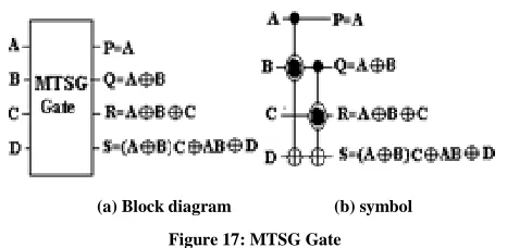
17) MTSG Gate:
The MTSG gate and its symbol is shown in fig 17 [30]. Quantum cost of MTSG gate is 6.
[image:5.612.51.284.161.275.2](a) Block diagram (b) symbol
Figure 17: MTSG Gate
18) SCL Gate:
[image:5.612.375.510.203.280.2]It is a 4x4 gate and its logic circuit is as shown in fig. [24].
Figure 18: Block diagram of SCL Gate
19) MKG Gate:
[image:5.612.90.248.329.413.2]The MKG gate is a 4X4 gate i.e. it comprises of four inputs and four outputs [31].
Figure 19: Block diagram of MKG Gate
20) HNG Gate:
The reversible HNG gate can work singly as a reversible full adder. If the input vector IV = (A, B, Cin, 0), then the output vector becomes OV = (P=A, Q=Cin, R=Sum, S=Cout)[28].
Figure 20: Block diagram of HNG Gate
21) BVF Gate:
This is a reversible double XOR gate and can be used for the duplication of the required inputs to meet the fan-out requirements. This gate is used to copy the operand bits and the number of gates required to copy is reduced by 50% with same quantum cost.[28]
Figure 21: Block diagram of BVF Gate
22) BME Gate:
The input vector is I(A,B,C,D) and the output vector is O(P,Q,R,S).[32]
Figure 22: Block diagram of BME Gate
23) DPG Gate:
It is a 4*4 Double Peres Gate. The input vector is I(A,B,C,D) and the output vector is O(P,Q,R,S). [32]
Figure 23: Block diagram of DPG Gate
24) DKG Gate:
[image:5.612.71.271.477.547.2]International Journal of Emerging Technology and Advanced Engineering
Website: www.ijetae.com (ISSN 2250-2459,ISO 9001:2008 Certified Journal, Volume 3, Issue 3, March 2013)
422
Figure 24: Block diagram of DKG Gate
25) PTR Gate:
[image:6.612.356.533.258.359.2]A 4* 4 reversible PTR gate can work as a reversible Full adder. [34]
Figure 25: Block diagram of PTR Gate
26) NCG[Nines compliment gate]:
[image:6.612.68.267.267.342.2]The key feature of this NCG is when control signal E is equal to zero, four bit binary number is directly passed to the output Q, R, S and T .When E is equal to one then, Q, R, S and T is equal to nines compliment of the number A,B, C and D. Therefore depending on control signal E, either passnine’s compliment outputs will be available on output Q, R, S and T.
Figure 26: NCG [Nines compliment gate]:
27) SBV Gate:
SBV gate is a 5 x 5 reversible gate. The fig 27 shows the proposed reversible logic gate which can individually work as a nines complementer with one garbage output [31].
Figure 27: SBV Gate
28) BSCL gate:
The purpose of this gateis either to find correction logic for BCD subtraction or to pass same data to the output depending on the control signal.Here F is the control signal ,if F is equal to 0 E A B C and D as it is passed to the output P Q R S and T. If F is equal to 1, then output Q R S and T depends on the value of E. If E is equal to 0 then Q R S and T is the nines compliment of the input binary number A B C and D. If E is equal to 1 then binary number 0001 is added to ABCD to get the valid corrected subtraction result.
Figure 28: BSCL Gate
IV. CONCLUSION AND FUTURE SCOPE
The reversible circuits form the basic building block of quantum computers. This paper presents the primitive reversible gates which are gathered from literature and this paper helps researches/designers in designing higher complex computing circuits using reversible gates. The paper can further be extended towards the digital design development using reversible logic circuits which are helpful in quantum computing, low power CMOS, nanotechnology, cryptography, optical computing, DNA computing, digital signal processing (DSP), quantum dot cellular automata, communication, computer graphics.
ACKNOWLEDGEMENT
We would like to express our sincere thanks to the anonymous reviewers for their critical suggestions which helped in improving the manuscript and also we express our gratitude to our respective faculty and our parents for supporting this work.
REFERENCES
[1] R. Landauer, ―Irreversibility and Heat Generation in the Computational Process‖, IBM Journal of Research and Development, 5, pp. 183-191, 1961.
[2] C.H. Bennett, ―Logical Reversibility of Computation‖, IBM J.Research and Development, pp. 525-532, November 1973. [3] Vlatko Vedral, Adriano Bareno and Artur Ekert, ―QUANTUM
[image:6.612.87.259.469.564.2]International Journal of Emerging Technology and Advanced Engineering
Website: www.ijetae.com (ISSN 2250-2459,ISO 9001:2008 Certified Journal, Volume 3, Issue 3, March 2013)
423
[4] Perkowski, M., A. Al-Rabadi, P. Kerntopf, A. Buller, M. Chrzanowska-Jeske, A. Mishchenko, M. Azad Khan, A. Coppola, S.Yanushkevich, V. Shmerko and L. Jozwiak, ―A general decomposition for reversible logic‖, Proc. RM’2001, Starkville, pp: 119-138, 2001..
[5] Perkowski, M. and P. Kerntopf, ―Reversible Logic. Invited tutorial‖, Proc. EURO-MICRO, Sept 2001, Warsaw, Poland.
[6] Hafiz Md. Hasan and A.R. Chowdhury, ―Design of Reversible Binary Coded decimal Adder by using Reversible 4 – bit Parallel Adder‖, VLSI Design 2005, pp. 255 – 260, Kolkata, India, Jan 2005. [7] B.Raghu kanth, B.Murali Krishna, M. Sridhar, V.G. Santhi Swaroop
―A DISTINGUISH BETWEEN REVERSIBLE AND
CONVENTIONAL LOGIC GATES ‖, International Journal of Engineering Research and Applications (IJERA) ISSN: 2248-9622 www.ijera.com Vol. 2, Issue 2,Mar-Apr 2012, pp.148-151 [8] Babu HMH, Islam MR, Chowdhury AR, Chowdhury SMA.
―Synthesis of full-adder circuit using reversible logic‖, 17th International Conference on VLSI Design 2004, 757-60.
[9] Ashis Kumer Biswas, Md. Mahmudul Hasan, Moshaddek Hasan, Ahsan Raja Chowdhury and Hafiz Md. Hasan Babu. ―A Novel Approach to Design BCD Adder and Carry Skip BCD Adder‖. 21st International Conference on VLSI Design, 1063-9667/08 $25.00 © 2008 IEEE DOI 10.1109/VLSI.2008.37.
[10] Abu Sadat Md. Sayem, Masashi Ueda.‖ Optimization of reversible sequential circuits‖. Journal of Computing, Volume 2, Issue 6, June 2010, ISSN 2151-9617.
[11] H.Thapliyal and N. Ranganathan, ―Design of reversible sequentialcircuits optimizing quantum cost, delay and garbage outputs,‖ ACMJournal of Emerging Technologies in Computing Systems, vol. 6, no.4, Article 14, pp. 14:1–14:35, Dec. 2010. [12] J.Smoline and David P.DiVincenzo, ―Five two-qubit gates are
sufficient to implement the quantum fredkin gate‖, Physics Review A, vol. 53, no.4, pp. 2855-2856,1996.
[13] H.R.Bhagyalakshmi, M.K.Venkatesha,‖ Optimized Reversible BCD adder using new Reversible Logic Gates‖, Journal of Computing, Vol 2, Issue 2, February 2010.
[14] M. Haghparast,K. Navi, ‖A Novel Reversible BCD Adder For Nanotechnology Based Systems‖, American Journal of Applied Sciences 5 (3): 282‐288, 2008,ISSN 1546‐ 9239.
[15] Abu Sadat Md. Sayem, Masashi Ueda.‖ Optimization of reversible sequential circuits‖. Journal ofComputing, Volume 2, Issue 6, June 2010, ISSN 2151-9617.
[16] M. Mohammadi and M. Eshghi. On figures of merit in reversible and quantum logic designs. Quantum Information Processing, 8(4):297– 318, Aug. 2009.
[17] Himanshu Thapliyal, Nagarajan Ranganathan, ―A New Reversible Design of BCD Adder‖ 978-3-9810801-7-9/DATE11/@2011 EDAA [18] R. Feynman,‖ Quantum Mechanical Computers‖, Optic News, Vol
11, pp 11-20 1985.
[19] Md. Belayet Ali , Md. Mosharof Hossin and Md. Eneyat Ullah, ―Design of Reversible Sequential Circuit UsingReversible Logic Synthesis‖ International Journal of VLSI design & Communication Systems (VLSICS) Vol.2, No.4, December 2011
[20] T.Toffoli,‖Reversible Computing‖ Tech memoMIT/LCS/TM-151, MIT Lab for Computer Science 1980.
[21] Fredkin E. Fredkin and T. Toffoli,‖Conservative Logic‖, Int’l J. Theoretical Physics Vol 21, pp.219-253, 1982
[22] Peres, ―Reversible Logic and Quantum Computers‖, Physical review A, 32:3266- 3276, 1985.
[23] Rakshith Saligram, Rakshith T.R, ―Novel Code Converter Employing Reversible logic‖,Volume 52– No.18, August 2012. [24] Majid Mohammadi, Mohammad Eshghi, Majid Haghparast and
Abbas Bahrololoom,‖Design and Optimization of Reversible BCD Adder/Subtractor Circuit for Quantum and Nanotechnology Based Systems‖, World Applied Sciences Journal 4 (6): 787-792, 2008 ISSN 1818-4952 © IDOSI Publications, 2008
[25] D.P.Vasudevan, P.K.Lala, J.Di and J.P.Parkerson, ― Reversible-logic design with online testability‖, IEEE Trans. on Instrumentation and Measurement, vol.55., no.2, pp.406- 414, April 2006.
[26] Nagamani A N#1, Jayashree H V#1,H R Bhagyalakshmi ―Novel Low Power Comparator Designusing Reversible Logic Gates‖, Indian Journal of Computer Science and Engineering (IJCSE) [27] V. Rajmohan, Member IACSIT, V. Renganathan, and M. Rajmohan
―A Novel Reversible Design of Unified Single Digit BCD Adder-Subtractor‖, International Journal of Computer Theory and Engineering, Vol. 3, No. 5, October 2011
[28] X. Susan Christina, M.Sangeetha Justine, K.Rekha, U.Subha and R.Sumathi, ―Realization of BCD adder using Reversible Logic‖, International Journal of Computer Theory and Engineering, Vol. 2, No. 3, June, 2010 1793-8201
[29] K. Biswas, M. M. Hasan, A. R. Chowdhury, and H. M. Hasan Babu,―Efficient approaches for designing reversible binary coded decimaladders,‖ Microelectron. J., vol. 39, no. 12, pp. 1693–1703, 2008.
[30] Sudharshan M, H R Bhagyalakshmi, M K Venkatesha, ― Novel Design of one digit high speed Carry select BCD Subtractor using Reversible logic gates‖, International Journal of Emerging Technology and Advanced Engineering (ISSN 2250-2459, Volume 2, Issue 7, July 2012)
[31] Md. Belayet Ali , Md. Mosharof Hossin and Md. Eneyat Ullah‖ Design of Reversible Sequential Circuit Using Reversible Logic Synthesis‖, International Journal of VLSI design & Communication Systems (VLSICS) Vol.2, No.4, December 2011
[32] B.Raghu kanth, B.Murali Krishna, M. Sridhar, V.G. Santhi Swaroop,‖ A DISTINGUISH BETWEEN REVERSIBLE AND CONVENTIONAL LOGIC GATES‖, International Journal of Engineering Research and Applications (IJERA) ISSN: 2248-9622 Vol. 2, Issue 2,Mar-Apr 2012, pp.148-151
![Figure 26: NCG [Nines compliment gate]:](https://thumb-us.123doks.com/thumbv2/123dok_us/8731750.887090/6.612.87.259.469.564/figure-ncg-nines-compliment-gate.webp)
