DEVELOPMENT OF P-RESONANT CONTROLLER FOR Z-SOURCE THREE PHASE INVERTER
AYOUB MEHDA
A thesis submitted in partial
fulfillment of the requirement for the award of the Degree of Master of Electrical and Electronic Engineering
Faculty of Electrical and Electronic Engineering Universiti Tun Hussein Onn Malaysia
iii
Specially dedicated to…
ACKNOWLEDGEMENT
I would like to express my sincere thanks to my Supervisor Dr. SHAMSUL
AIZAM BIN ZULKIFLI for his friendly welcome and for his open and warm
attitude, with the unlimited help from him. Also, I am indebted to my mentors, in Faculty of Electrical and Electronics Engineering for their attention and time.
I would also like to thank all of my colleagues in the university especially the students of Electrical and Electronics for their friendship, encouragement and technical advice, and who have made my time enjoyable by providing a pleasant environment.
I would like to thank my sweet family, specially my parents. Although far away in Algeria, they always concentrate me on my life here and gave me great support, encouragement and love. I can feel their selfless love all the time.
As it is impossible to mention in this brief acknowledgment every single person, I would like to thank all those who have contributed in a way or another to this achievement.
vii
ABSTRACT
CONTENTS
TITLE i
DECLARATION ii
DEDICATION iii
ACKNOWLEDGEMEN vi
ABSTRACT vii
TABLE OF CONTENTS viii
LIST OF FIGURES xii
LIST OF SYMBOLS AND ABBREVIATIONS xv
CHAPTER 1 INTRODUCTION 1
1.1 Introduction 1
1.2 Background of Project 2
1.3 Problem statement 3
1.4 Project objectives 4
1.5 Project scopes 4
1.6 Project structure outlines 4
CHAPTER 2 LITERATURE REVIEW 6
2.1. Overview of inverters 6
2.1.1 Application of inverter 6
ix 2.2.1 Three phase current source inverter 8 2.2.2 Three phase voltage source inverter 10 2.2.3 Disadvantages of (VSI and CSI) 11
2.3 Z-source inverter 11
2.3.1 Single phase Z-source inverter 12 2.3.2 Three phase Z-source inverter 12
2.3.3 Advantages of ZSI 16
2.4 Sinusoidal PWM in three phase voltage source
inverters 16
2.4.1 The Pulse Width Modulation signal 17
2.5 Closed-loop control systems 18
2.5.1 Effect of feedback 19
2.5.2 Advantages and disadvantages of closed
loop control system 20
2.6 Type of controller 20
2.6.1 Fuzzy logic controller 21
2.6.2 PI controller 22
2.6.3 PID controller 23
2.6.4 P-Resonant controller 24
2.7 Simulation tools 25
2.7.1 MATLAB 25
2.7.2 SILULINK 26
2.8 Related work of Z-source and P-Resonant controller 26
CHAPTER 3 RESEARCH METHODOLOGY 28
3.1 Introduction 28
3.2 Project block diagram 29
3.3 Project flowchart 30
3.4 Simulation and analysis Tools 31
3.5.1 Design the capacitor of the Z-Source network 33 3.5.2 Design the inductor of the Z-Source network 33 3.6 Proportional Resonant Controller 34 3.7 Design and simulation of the simulink blocks 36
3.7.1 DC source model 36
3.7.2 Z-Source network model
37 3.7.3 Three phase inverter mode 38 3.7.4 P-resonant current and voltage model
39 3.8 Design and simulation of the overall circuit diagram
40 3.9 Simulation parameters
41
CHAPTER 4 RESULTS AND ANALYSIS 42
4.1 Introduction
42 4.2 System design and simulation
43 4.3 Circuit simulation of Z-source three phase inverter
43 4.3.1 Open loop Z-source three phase inverter by
using Simulink 44
4.4 Analysis for open loop Z-source three phase inverter 44 4.5 Simulation results with P-Resonant controller 47 4.5.1 Data simulation results 48 4.5.1.1 At Reference Current iR = 2A 48 4.5.1.2 At Reference Current iR=2.5A 50 4.5.1.3 At Reference Voltage VR= 200V 52 4.5.1.4 At Reference Voltage VR= 250V 55 4.6 THD comparison with P-Resonant controller
xi 4.7 Three phase Z-source inverter with PI current
controller 59
4.7.1 At Reference Current 𝒊𝑷 = 2A
59 4.7.2 At Reference Current 𝒊𝑷 = 2.5A
60 4.8 Comparison between PR current controller with PI
current controller 62
CHAPTER 5 CONCLUSION AND FUTURE WORKS 63
5.1 Conclusion 63
5.2 Future works 64
LIST OF FIGURES
1.1 Project block diagram 3
2.1 Traditional Current-source inverter 9
2.2 Traditional V-source inverter 11
2.3 Single-phase full bridge Z-Source inverter 12
2.4 Z-source inverter 13
2.5 Equivalent circuit of the Z-source inverter viewed from the dc link 13 2.6 Equivalent circuit of the Z-source inverter viewed from the dc link when the
inverter bridge is in the shoot-through zero state 14 2.7 Equivalent circuit of the Z-source inverter viewed from the dc link when the
inverter bridge is in one of the eight nonshoot-through switching states 14
2.8 Block diagram for generation of SPWM pulses 17
2.9 PWM Signal 17
2.10 Block diagram of a closed loop control system 18
2.11 Closed loop control system 19
2.12 Block Diagram of feedback 20
2.13 Fuzzy logic controller 21
2.14 Block diagram of PI controller 22
2.15 Block diagram of a PID controller 23
2.16 P-resonant controller 24
3.1 Project block diagram 29
3.2 Project flow chart 30
xiii
3.4 P-R controller design 35
3.5 System design and blocks simulation 36
3.6 The DC source model 37
3.7 Z-Source Network model 37
3.8 Three phase inverter model 38
3.9 P-resonant current control and Pulse Withed Modulation (PWM) 39
3.10 P- resonant current control 39
3.11 Overall circuit diagram 40
4.1 System design and Simulation 43
4.2 Simulation open loop Z-source three phase inverter by using MATLAB software. 44
4.3 DC voltage source (400V) 45
4.4 Output voltage of Z-source network 45
4.5 Output voltage of Z-source three phase inverter 46
4.6 Output voltage of open loop circuit Z-source three phase inverter (filter) 46
4.7 Output current of open loop circuit Z-source three phase inverter (filter) 47
4.8 P-Resonant controls the output current. 48
4.9 Reference current iR= 2A 49
4.10 Output current of Z-source three phase inverter (filter) with PR Controller when reference current iR= 2A 49
4.11 Error signal when iR= 2A 50
4.12 Reference current iR= 2.5A 51
4.13 Output current of Z-source three phase inverter (filter) with PR Controller when reference current iR= 2.5A 51
4.14 Error signal when iR= 2.5A 52
4.15 P-Resonant controls the output voltage. 53
4.16 Reference voltage at VR= 200V 53
4.17 Output voltage of Z-source three phase inverter (filter) with PR Controller when reference voltage VR= 200V 54
4.18 Error signal when VR= 200V 54
4.19 Reference voltage at VR= 250V 55
4.21 Error signal when VR= 250V 56
4.22 The THD when reference current iR= 2A 57
4.23 The THD when reference current iR= 2.5A 57
4.24 The THD reference voltage VR= 200V 58
4.25 The THD reference voltage VR= 250V 58
4.26 Output current of Z-source three phase inverter (filter) with PI Controller when reference current iP= 2A 59
4.27 Error signal when ip= 2A 60
4.28 Output current of Z-source three phase inverter (filter) with PI Controller when reference current iP= 2.5A 61
xv
LIST OF SYMBOLS AND ABBREVIATIONS
DC direct current
AC alternating current VSI voltage source inverter CSI Currentsource inverter ZSI Z-source inverter PR Proportional Resonant PWM Pulse Width Modulation
SPWM sinusoidal pulse-width modulation PI Proportional integral
PID Proportional Integral Derivative PD Proportional Derivative
CHAPTER 1
INTRODUCTION
This chapter discusses the background of the research, the objectives of project, problem statement and scopes of study.
1.1 Introduction
2
1.2 Background of Project
The power inverter is an electronic device that can transform a direct current (DC) into alternating current (AC) at a given voltage and frequency. The inverters are used in photovoltaic off-grid (stand alone) for powering electric remote houses, mountain chalets, mobile homes, boats and are also used in grid-connected photovoltaic systems to enter the current produced by the plant directly into the power grid distribution (solar inverters). The inverters are also used in many other applications, ranging from UPS to speed controllers for electric motors, from power supplies switching to lighting. By the term "inverter" is designed to include a group "rectifier-inverter", supplied with alternating current and used to vary the voltage and the frequency of the alternating current output as a function of the incoming (eg for the supply of particular machinery). The most common inverters used to power the AC loads are of three types: square wave inverter (suitable for resistive loads), modified sine wave inverter (suitable for resistive, capacitive, inductive loads can produce noise) and pure sine wave inverter (suitable for all types of loads because faithfully reproduce a sine wave equal to that of our domestic power supply).
Three-phase inverters are used for variable-frequency drive applications and for high power applications such as HVDC power transmission. A basic three-phase inverter consists of three single-phase inverter switches each connected to one of the three load terminals. For the most basic control scheme, the operation of three switches is coordinated so that one switch operates at each600 point of the fundamental output waveform. This creates a line-to-line output waveform that has six steps. The six steps waveform has a zero-voltage step between the positive and negative sections of the square-wave such that the harmonics that are multiples of three are eliminated as described above. When carrier-based PWM techniques are applied to six step waveforms, the basic overall shapes, or envelope, of the waveform is retained so that third harmonic and its multiples are cancelled [2].
voltage, which improves the inverter reliability greatly, and provides an attractive single stage dc to ac conversion that is able to buck and boost the voltage. The shoot-through duty cycle is used for controlling the dc link voltage boost and hence the output voltage boost of the inverter [3].
[image:15.595.128.518.338.506.2]P-Resonant (PR) controller gained a large popularity in recent years in current regulation of grid-tied systems. It introduces an infinite gain at a selected resonant frequency for eliminating steady-state error or current harmonics at the frequency. However the harmonic compensators of the P-Resonant controllers are limited to several low-order current harmonics, due to the system instability when the compensated frequency is out of the bandwidth of the systems [4].
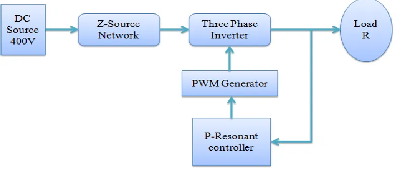
Figure 1.1: Project block diagram.
1.3 Problem Statement
Z-Source inverter widely used in many applications that required high controlled. In controlling Z-source inverter current/voltage, there are several ways can be used as conventional PI or PD become a suitable solution. However, the capabilities of these controllers are limited and the performance is not the best possible.
4 Z-source inverter (ZSI), which is based on Z-source network, can buck and boost the output AC voltage, which is not possible using traditional voltage source or current source inverters. Z-source can have greater output AC voltage than the input, wish is not possible using traditional voltage source or current source inverters.
1.4 Project objectives
The objectives of this project are:
1. to develop and simulate the three-phase Z-Source inverter. 2. to boost the output voltage of the three-phase Z-Source inverter.
3. to develop P-Resonant controller that suitable for three Z-Source inverter. 4. to control the output current and voltage of Z-Source three phase inverter and
reduce the steady state error.
1.5 Project scopes
This project is concerned with the scopes as follows:
1. Presenting and modeling of the three-phase Z-Source inverter that will be modeled using MATLAB Simulink software.
2. P-Resonant control with Sinusoidal Pulse width Modulation (SPWM) technique will be used to control the switching signals.
1.6 Project Structure Outlines
This project consists of five chapters.
Chapter 2 summarized the information of the related previous studies on the Z-Source inverter. In addition, the chapter covers the block diagrams and implementation model of the inverters and the controllers. It is covers also the comprehensive of the controller problems.
Chapter 3 discusses the methodology of implementation the three phase Z-Source inverter with P-Resonant controller and design it using MATLAB simulink.
Chapter 4 presents the results and analysis of Z-Source three phase inverter and introduces the results with analysis of P-Resonant controller with different situations of reference current and reference voltage.
6
CHAPTER 2
LITERATURE REVIEW
This chapter summarizes the information of the related previous studies on inverters on general and Z-Source Inverter. In addition, the chapter covers types of most inverters, the related topologies, the effective control technique methods. The base comments and their detailed functions will be introduced and discussed. These reviews are done based on materials from journals, conference proceeding and books.
2.1 Overview of Inverters
A power inverter, or inverter, is an electronic device or circuitry that changes direct current (DC) to alternating current (AC) [5]. The input voltage, output voltage and frequency, and overall power handling depend on the design of the specific device or circuitry.
2.1.1 Applications of Inverter
effects (such as a rotary apparatus) and electronic circuitry. Static inverters do not use moving parts in the conversion process [6]. The inverters have been used in many applications, such as DC power source utilization, an inverter converts the DC electricity from sources such as batteries or fuel cells to AC electricity. The electricity can be at any required voltage; in particular it can operate AC equipment designed for mains operation, or rectified to produce DC at any desired voltage [5]. In addition, they are used in Uninterruptible power supplies. An uninterruptible power supply (UPS) uses batteries and an inverter to supply AC power when main power is not available. When main power is restored, a rectifier supplies DC power to recharge the batteries. Moreover, the inverters are used in Electric motor speed control. Inverter circuits designed to produce a variable output voltage range are often used within motor speed controllers. The DC power for the inverter section can be derived from a normal AC wall outlet or some other source. Control and feedback circuitry is used to adjust the final output of the inverter section which will ultimately determine the speed of the motor operating under its mechanical load. Motor speed control needs are numerous and include things like: industrial motor driven equipment, electric vehicles, rail transport systems, and power tools. Switching states are developed for positive, negative and zero voltages. The generated gate pulses are given to each switch in accordance with the developed pattern and thus the output is obtained [1]. Furthermore, they are utilized in Power grid. Grid-tied inverters are designed to feed into the electric power distribution system. They transfer synchronously with the line and have as little harmonic content as possible. They also need a means of detecting the presence of utility power for safety reasons, so as not to continue to dangerously feed power to the grid during a power outage.
8 improve the overall efficiency of the system. The output from several micro inverters is then combined and often fed to the electrical grid [7]. Rather than energy solar the HVDC is used. With HVDC power transmission, AC power is rectified and high voltage DC power is transmitted to another location. At the receiving location, an inverter in a static inverter plant converts the power back to AC. The inverter must be synchronized with grid frequency and phase and minimize harmonic generation [8].
2.2 Inverter
The inverters have different topologies and the most known topologies are three phase current source inverter (abbreviated as I-source converter) and three phase voltage source inverter (abbreviated as V-source converter). In the I-source converter we deal with the current in the analysis of the performance. However, the performance analysis of the V-source converter is depended on the voltage. These two types will be explained in the next subsection.
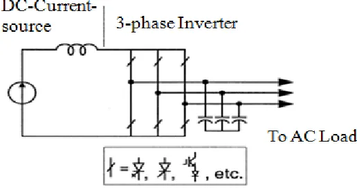
2.2.1 Three Phase Current Source Inverter
Figure 2.1 shows the current-source converter (abbreviated as I-source converter) structure. A dc current source feeds the main converter circuit, a three-phase bridge. The dc current source can be a relatively large dc inductor fed by a voltage source such as a battery, fuel-cell stack, diode rectifier, or thyristor converter. Six switches are used in the main circuit, each is traditionally composed of a semiconductor switching device with reverse block capability such as a gate-turn-off thyristor (GTO) and SCR or a power [9].
The ac output voltage has to be greater than the original dc voltage that feeds the dc inductor or the dc voltage produced is always smaller than the ac input voltage. Therefore, the I-source inverter is a boost inverter for dc-to-ac power conversion and the I-source converter is a buck rectifier (or buck converter) for ac-to-dc power conversion. For applications where a wide voltage range is desirable, an additional dc–dc buck (or boost) converter is needed. The additional power conversion stage increases system cost and lowers efficiency [9].
At least one of the upper devices and one of the lower devices have to be gated on and maintained on at any time. Otherwise, an open circuit of the dc inductor would occur and destroy the devices. The open-circuit problem by EMI noise’s misgating-off is a major concern of the converter’s reliability. Overlap time for safe current commutation is needed in the Current-source converter, which also causes waveform distortion, etc [10].
The main switches of the Current-source converter have to block reverse voltage that requires a series diode to be used in combination with high-speed and high-performance transistors such as insulated gate bipolar transistors (IGBTs).
[image:21.595.183.441.510.649.2]This prevents the direct use of low-cost and high-performance IGBT modules and intelligent power modules (IPMs) [11].
10
2.2.2 Three Phase Voltage Source Inverter
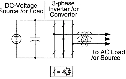
Figure 2.2 shows the Voltage-source converter (abbreviated as V-source converter) structure. A dc voltage source supported by a relatively large capacitor feeds the main converter circuit, a three-phase bridge.
The dc voltage source can be a battery, fuel-cell stack, diode rectifier, and/or capacitor. Six switches are used in the main circuit; each is traditionally composed of a power transistor and an antiparallel (or freewheeling) diode to provide bidirectional current flow and unidirectional voltage blocking capability. The V-source converter is widely used. It, however, has the following conceptual and theoretical barriers and limitations [12].
The ac output voltage is limited below and cannot exceed the dc-rail voltage or the dc-rail voltage has to be greater than the ac input voltage. Therefore, the V-source inverter is a buck (step-down) inverter for dc-to-ac power conversion and the V-source converter is a boost (step-up) rectifier (or boost converter) for ac-to-dc power conversion. For applications where over drive is desirable and the available dc voltage is limited, an additional dc-dc boost converter is needed to obtain a desired ac output. The additional power converter stage increases system cost and lowers efficiency [10].
The upper and lower devices of each phase leg cannot be gated on simultaneously either by purpose or by EMI noise. Otherwise, a shoot-through would occur and destroy the devices. The shoot-through problem by electromagnetic interference (EMI) noise’s misgating-on is a major killer to the converter’s reliability. Dead time to block both upper and lower devices has to be provided in the V-source converter, which causes waveform distortion.
Figure 2.2: Traditional V-source inverter.
2.2.3 Disadvantages of Current Source Inverter (VSI) and Voltage Source
Inverter (CSI)
Typical inverters (VSI and CSI) have few disadvantages as Behave in a boost or buck operation only. Thus the obtainable output voltage range is limited, either smaller or greater than the input voltage. Vulnerable to EMI noise and the devices gets damaged in either open or short circuit conditions. The combined system of DC-DC boost converter and the inverter has lower reliability. The main switching device of VSI and CSI are not interchangeable [14].
2.3 Z-Source Inverter
12 2.3.1 Single Phase Z-Source Inverter
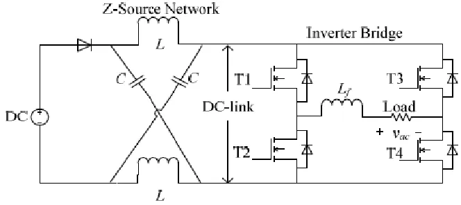
[image:24.595.148.480.224.372.2]The Z-Source inverter [16] provides a single-stage topology for both voltage boosting and inversion. The topology of single-phase full bridge Z-Source inverter is shown in Figure 2.3.
Figure 2.3: Single-phase full bridge Z-Source inverter.
The DC-side of a conventional single-phase full bridge voltage source inverter is modified with a unique X-shape impedance network, which is known as the Z-Source network. Therefore, shoot-through state, which is strictly forbidden in conventional voltage source inverters, is allowed and implemented here for voltage boosting purposes. Since the capacitor in the Z-Source network may be charged to a higher voltage than the DC source, a diode is connected to prevent possible discharging. To realize the bidirectional power flow characteristic, the diode can be replaced with an IGBT with anti-paralleled diode to form a bidirectional Z-Source converter [17].
2.3.2 Three Phase Z-Source Inverter
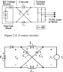
operating principle and control of the Z-Source inverter in Figure 2.4. In Figure 2.4, the three-phase Z-Source inverter bridge has nine permissible switching states (vectors) unlike the traditional three-phase V-source inverter that has eight. The traditional three-phase V-source inverter has six active vectors when the dc voltage is impressed across the load and two zero vectors when the load terminals are shorted through either the lower or upper three devices, respectively. However, the three-phase Z-Source inverter bridge has one extra zero state when the load terminals are shorted through both the upper and lower devices of any one phase leg (i.e., both devices are gated on),any two phase legs, or all three phase legs [16,17].
[image:25.595.191.448.294.586.2]Figure 2.4: Z-source inverter
14
Figure 2.6: Equivalent circuit shoot-through zero state of the Z-source inverter viewed from the dc link.
Figure 2.7: Equivalent circuit nonshoot-through switching states of the Z-source inverter viewed from the dc link.
[image:26.595.175.461.316.481.2]current source as shown in Figure 2.7 when in one of the six active states. Note that the inverter bridge can be also represented by a current source with zero value (i.e., an open circuit) when it is in one of the two traditional zero states. Therefore, Figure 2.7 shows the equivalent circuit of the Z-Source inverter viewed from the dc link when the inverter bridge is in one of the eight nonshoot-through switching states [18].
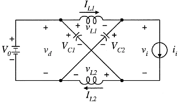
Switching between shoot-through states and non shootthrough states allows boost voltage of capacitors 𝑈𝐶 and voltage of the inverter bridge over input voltage 𝑈𝑖𝑛 . During the design of ISI the most challenging is the estimation of values of the reactive components of the impedance network [19]. The component values should be evaluated for the minimum input voltage of the converter, where the boost factor and the current stresses of the components become maximal. Calculation of the average current of an inductor.
𝐼𝐿 = 𝑃 𝑈𝑖𝑛
(2.1)
The maximum current through the inductor occurs when the maximum shoot-through happens, which causes maximum ripple current. In our design, 60% peak-to-peak current ripple through the Z-source inductor during maximum power operation was chosen. Therefore, the allowed ripple current is ∆𝐼𝐿 , and the maximum current through the inductor is 𝐼𝐿 𝑚𝑎𝑥:
𝐼𝐿 𝑚𝑎𝑥 = 𝐼𝐿 + 𝐼𝐿 . 30% (2.2)
𝐼𝐿 𝑚𝑖𝑛 = 𝐼𝐿 − 𝐼𝐿 . 30% (2.3)
∆𝐼𝐿 = 𝐼𝐿 𝑚𝑎𝑥− 𝐼𝐿 𝑚𝑖𝑛 (2.4)
The boost factor of the input voltage is: 𝐵 = 1
1 − 2𝐷𝑍 = 𝑈𝑖𝑛1
𝑈𝑖𝑛 (2.5)
Where D0 is the shoot-through duty cycle: 𝐷𝑍 =
𝐵 − 1
1 − 2𝐵 (2.6) The capacitor voltage during that condition is
𝑈𝐶 =
𝑈𝑖𝑛 + 𝑈𝑖𝑛1
16 Calculation of required inductance of Z-source inductors:
𝐿 = 𝑇𝑍 . 𝑈𝐶 ∆𝐼𝐿
(2.8)
Where T0 - is the shoot-through period per switching cycle:
𝑇𝑍 = 𝐷𝑍 . 𝑇 (2.9)
Calculation of required capacitance of Z-source capacitors: 𝐶 = 𝐼𝐿 . 𝑇𝑍
𝑈𝐶 . 3% (2.10)
2.3.3 Advantages of ZSI
Z-Source inverter (ZSI), which is based on Z-Source network, can buck and boost the output AC voltage, which is not possible using traditional voltage source or current source inverters. Also, the ZSI has the unique ability to allow the dc-link of the inverter to be shorted, which is not possible in the traditional voltage source inverters. This improves the reliability of the circuit [15]. Z-Source inverter has the unique feature that it can boost the output voltage by introducing shoot through operation mode, which is forbidden in traditional voltage source inverters. With this unique feature, the Z-Source inverter provides a cheaper, simpler, single stage approach for applications of fuel cell. Moreover, it highly enhances the reliability of the inverter because the shoot through can no longer destroy the inverter [9-15].
2.4 Sinusoidal PWM in Three-Phase Voltage Source Inverters
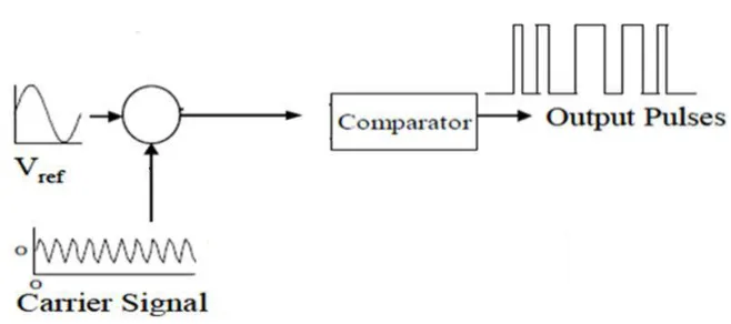
sinusoidal waveform by filtering an output pulse waveform with varying width. A high switching frequency leads to a better filtered sinusoidal output waveform. The variations in the amplitude and frequency of the reference voltage change the pulse-width patterns of the output voltage but keep the sinusoidal modulation. As shown in Figure 2.8.
Figure 2.8: Block diagram for generation of SPWM pulses
2.4.1 The Pulse Width Modulation Signal
This is how a PWM signal would look like
[image:29.595.211.427.531.598.2]18 A Pulse Width Modulation (PWM) Signal is a method for generating an analog signal using a digital source. A PWM signal consists of two main components that define its behavior: a duty cycle and a frequency. The duty cycle describes the amount of time the signal is in a high (on) state as a percentage of the total time of it takes to complete one cycle. The frequency determines how fast the PWM completes a cycle (i.e. 1000 Hz would be 1000 cycles per second), and therefore how fast it switches between high and low states. By cycling a digital signal off and on at a fast enough rate, and with a certain duty cycle, the output will appear to behave like a constant voltage analog signal when providing power to devices [20].
2.5 Closed-loop control systems
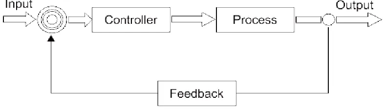
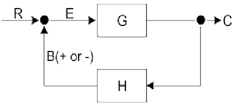
[image:30.595.126.520.536.648.2]Control system in which the output has an effect on the input quantity in such a manner that the input quantity will adjust itself based on the output generated is called closed loop control system. Open loop control system can be converted in to closed loop control system by providing a feedback. This feedback automatically makes the suitable changes in the output due to external disturbance [21]. In this way closed loop control system is called automatic control system. Figure 2.10 shows the block diagram of closed loop control system in which feedback is taken from output and fed in to input [22].
Figure 2.10: Block diagram of a closed loop control system
In any control system, output is affected due to change in environmental condition or any kind of disturbance. So one signal is taken from output and is fed back to the input. This signal is compared with reference input and then error signal is generated. This error signal is applied to controller and output is corrected. Such a system is called feedback system. Figure 2.11 shows the block diagram of feedback system [23].
Figure 2.11: Closed loop control system
When feedback signal is positive then system called positive feedback system. For positive feedback system, the error signal is the addition of reference input signal and feedback signal. When feedback signal is negative then system is called negative feedback system. For negative feedback system, the error signal is given by difference of reference input signal and feedback signal.
2.5.1 Effect of Feedback
20
Figure 2.12: Block Diagram
2.5.2 Advantages and Disadvantages of Closed Loop Control System
Closed loop control systems are more accurate even in the presence of non-linearity. It has highly accurate as any error arising is corrected due to presence of feedback signal. The sensitivity of system may be made small to make system more stable. Closed loop is less affected by noise.
The closed loop control systems are costlier. They are complicated to design. Feedback leads to oscillatory response. Overall gain is reduced due to presence of feedback. Stability is the major problem and more care is needed to design a stable closed loop system.
2.6 Types of Controller
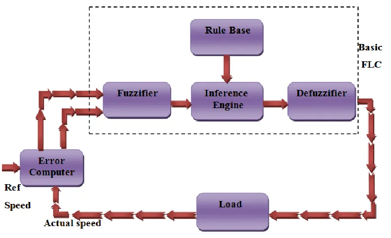
2.6.1 Fuzzy Logic Controller
[image:33.595.113.508.390.631.2]Fuzzy logic controller which is presented by Zadeh in 1965, is a new controller. Besides that, fuzzy logic controller is more efficient from the other controller such as proportional-integral (PI) controller [24]. Fuzzy Logic Control (FLC) technique has been used for over twenty years with many successful applications. It is an ideal technique for complex systems that are difficult to model or that present important parameter variation. FLC design focuses in gaining a basic understanding of the plant in order to design an appropriate set of rules that can be directly loaded into the fuzzy controller [25]. Figure 2.13 shows the basic structure of fuzzy logic controller. Fuzzy logic’s linguistic terms are most often expressed in the form of logical implications, such as If then rules. These rules define a range of values known as fuzzy membership functions [26].
Figure 2.13: Fuzzy logic controller
22 these features, the fuzzy logic is applied to the control field, and the fuzzy logic control has become a field of intelligent control and one of the emerging parts of the research. Fuzzy logic controllers and application are used in many engineering applications where the control systems are difficult to model [26].
2.6.2 Proportional Integral ( PI ) Controller
[image:34.595.150.548.439.616.2]PI controller will eliminate forced oscillations and steady state error resulting in operation of on-off controller and P controller respectively. However, introducing integral mode has a negative effect on speed of the response and overall stability of the system. Thus, PI controller will not increase the speed of response. It can be expected since PI controller does not have means to predict what will happen with the error in near future. This problem can be solved by introducing derivative mode which has ability to predict what will happen with the error in near future and thus to decrease a reaction time of the controller [27]. Figure 2.14 shows the basic structure of PI controller.
Figure 2.14: Block diagram of PI controller
obtain the desired loop gain, crossover frequency and phase margin. The stability of the system is guaranteed by an adequate phase margin. However, linear PID and PI controllers can only be designed for one nominal operating point. A boost converter’s small signal model changes when the operating point varies. The poles and a right-half plane zero, as well as the magnitude of the frequency response, are all dependent on the duty cycle. Therefore, it is difficult for the PID controller to respond well to changes in operating point. The PI controller is designed for the boost converter for operation during a start-up transient and steady state respectively [27].
𝐾(𝑆) = 𝐾𝑝+ 𝐾𝑖
𝑠 (2.11)
2.6.3 Proportional Integral Derivative (PID) Controller
[image:35.595.117.498.533.713.2]PID controller has all the necessary dynamics: fast reaction on change of the controller input (D mode), increase in control signal to lead error towards zero (I mode) and suitable action inside control error area to eliminate oscillations (P mode). Derivative mode improves stability of the system and enables increase in gain K and decrease in integral time constant Ti, which increases speed of the controller response. Figure 2.15 shows the basic structure of PID controller.
24 PID controller is used when dealing with higher order capacitive processes (processes with more than one energy storage) when their dynamic is not similar to the dynamics of an integrator (like in many thermal processes). PID controller is often used in industry, but also in the control of mobile objects (course and trajectory following included) when stability and precise reference following are required. Conventional autopilot is for the most part PID type controllers [24].
𝐾(𝑆) = 𝐾𝑝+ 𝐾𝑖
𝑠 + 𝐾𝑑 𝑆 (2.12)
2.6.4 P-Resonant Controller
[image:36.595.137.503.488.624.2]This controller aims to get a good reference tracking and to reduce the output voltage harmonic distortion when the inverter feeds linear and nonlinear loads. The resonant controller is a generalized PI controller that is able to control not only DC but also AC variables. Figure 2.16 shows the structure of the resonant controller [28].
Figure 2.16: P-resonant controller
In addition to a forward integrator there is another integrator in the feedback loop. The transfer function is given by
𝐺𝑃𝑅 = 𝐾𝑝+ 𝐾𝑖 s 𝑠2+ 𝜔
0𝟐