© 2017, IRJET | Impact Factor value: 5.181 | ISO 9001:2008 Certified Journal | Page 348
Abstract
-This paper presents a single phase 5 level FlyingCapacitor Multilevel Inverter. In order to obtain multilevel output voltage waveforms, a switching strategy based on calculating switching angles is explained. Simulation and experimental results of multilevel voltage waveforms are given for 5 levels. The one phase leg of five level Flying Capacitor Multilevel Inverter is shown in this paper and the steps to synthesize the five level voltages is given. The Simulation block diagram and triggering diagram of the circuit is explained.
Keyword
–
Flying capacitor, multilevel inverter. Matlab/Simulink.1. INTRODUCTION
[4]The advancement in the field of power electronic has increased the usage of high power medium voltage drive applications in the industrial arena. In order to get better performance of medium voltage and high power electric drive, the dv/dt and the harmonic should be minimized by the introduction of more levels in the output voltage. This has initialized the theory of multilevel inverter for industrial drive to overcome the above disadvantages. In multilevel inverter the output voltage are generated at high frequency and low switching frequency with low distortions. In case of high power and medium voltage situation such as laminators, SVC, HVDC Pumps, blowers , compressors and so on. Multilevel inverter plays an important role in the area of electronic and it is widely used in industrial and renewable energy applications for converting dc to ac. It not only achieves high power rating but also enables the use of renewable energy source. There are several configurations available for forming the multilevel inverter.
1. Diode clamped multilevel inverter
2. Flying capacitor clamped multilevel inverter 3. Cascade H-bridge multilevel inverter.
Flying capacitor multilevel inverter usage of extra capacitor clamped to the power switches phase rail to provide the dc
voltage level. The structure allow for the inverter to supply high capabilities especially during the power outages due to reducing the switching states providing by clamping capacitor.
2 .FIVE LEVEL FLYING CAPACITOR MULTILEVEL
INVERTER
The main concept of this inverter is to use capacitors. It is of series connection of capacitor clamped switching cells. The capacitors transfer the limited amount of voltage to electrical devices. In this inverter switching states are like in the diode
clamped inverter. Clamping diodes are not required in this type of multilevel inverters. The output is half of the input DC voltage. It is drawback of the flying capacitors multi level inverter. It also has the switching redundancy within phase to balance the flaying capacitors. It can control both the active and reactive power flow. But due to the high frequency switching, switching losses will takes place[5,6].
BASIC FEATURES:
The topology consists of diodes, capacitors and switching devices. Although theoretically this topology has been designed to give infinite levels, but due to practical limitations this only gives up to six levels of voltage.Each leg consists of switching devices which are generally transistors. Capacitors nearer to the load have lower voltage.Capacitors nearer to the source voltage (Vdc) have
higher voltage.The number of level depends upon the number of conducting switches in each limb.
CALCULATION:
The formula to find number of devices needed for obtaining five level multilevel inverter is
An ‘n’ level inverter needs:
• Number of voltage sources Ndc = (n-1)
• Number of switching devices Nsd = 2(n-1)
• Number of balancing capacitors Nbc = 1)
(n-2)/2
A 5-Level Single Phase Flying Capacitor Multilevel Inverter
Sayli Khadse
1,Rohini Mendole
2,Amarjeet Pandey
31
Sayli Khadse Dept. of Electrical Engineering,S.B.J.I.T.M.R,Nagpur,Maharashtra,India.
2Rohini Mendole Dept. of Electrical Engineering,S.B.J.I.T.M.R, Nagpur,Maharashtra,India.
3Amarjeet.S.Pandey, Dept. of Electrical Engineering, S.B.J.I.T.M.R,Nagpur,Maharashtra,India.
© 2017, IRJET | Impact Factor value: 5.181 | ISO 9001:2008 Certified Journal | Page 349
• Number of DC bus capacitors Nc = (n-1)In a five level flying capacitor inverter: N = 5
Therefore: Ndc = (5-1) = 4
Nsd = 2(5-1) = 8
Nbc = (5-1) (5-2)/2 = 6
Nc = (5-1) = 4
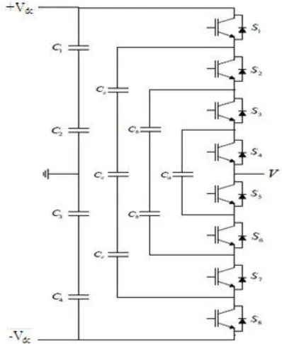
The following one phase leg of a five level flying capacitor multilevel inverter to produce a staircase output voltage is shown below
FIG(1)ONE PHASE OF A FIVE LEVEL FLYING CAPACITOR MULTILEVEL INVERTER
OPERATION:
For an output voltage level V0 = Vdc, turn on all upper half
switches S1 through S4.For an output voltage level V0 =
Vdc/2, turn on three upper switches S1 through S3 and one
lower switch S5.For an output voltage level V0 = 0, turn on
two upper switches S1 & S2 and two lower switch S5 & S6.For an output voltage level V0 = -Vdc/2, turn on one
upper switch S1 and three lower switches S5 through S7. For an output voltage level V0 = -Vdc, turn on all lower half
switches S5 through S8.
Table 1 shows the voltage levels and their corresponding switch states. State condition 1 means the switch is on, and state 0 means the switch is off.[1]
TABLE 1: THE SWITCHING STATE OF FLYING LEVEL MULTILEVEL INVERTER
V0 S1 S2 S3 S4 S5 S5 S5 S8
Vdc 1 1 1 1 0 0 0 0
Vdc/2 1 1 1 0 1 1 1 0
0 1 1 0 0 1 1 1 0
-Vdc/2 1 0 0 0 1 1 1 0 -V
dc 1 0 0 0 1 1 1 1
SIMULATION :
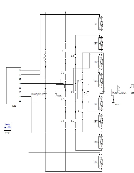
The whole research has been carried out to find out about the performance of single phase five level multilevel inverter using MATLAB/SIMULINK simulation software. Matlab/ Simulink is software for modeling, simulating, and analyzing. It supports linear and nonlinear systems, modeled in continuous time, sampled time. The simulation process is performed on circuit having two different switches i.e IDEAL switch and IGBT switch.The working procedure is same in both the type of switches[3,10].
SIMULINK MODEL USING IDEAL SWITCH
[image:2.612.43.242.302.544.2]© 2017, IRJET | Impact Factor value: 5.181 | ISO 9001:2008 Certified Journal | Page 350
FIG (2) SIMULINK MODEL USING IDEAL SWITCHSIMULINK MODEL USING IGBT SWITCH
The simulation is then performed using IGBT switch.The main advantages of IGBT compared with various kinds of transistors are low ON resistance, high voltage -capacity, fast switching speed, ease of drive and joined with zero gate drive current creates a good option for sensible speed, and various high voltage applications like PWM, SMPS, variable speed control, AC to DC converter powered by solar and frequency converter applications which operates with a hundred’s of KHz. The main disadvantages are: The speed of the Switching is lower to a Power MOSFET and higher to a BJT.[10]
FIG (3) SIMULINK MODEL USING IGBT SWITCH
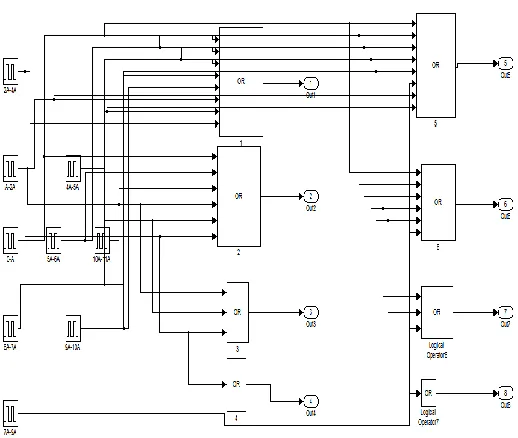
TRIGGERING OF SWITCHES:
In the triggering circuit, basically for generating pulses OR GATE logic is used.In the triggering circuit there are total 8 OR gate are used in which 4 OR gates are used for positive half cycle and other 4 OR gates for negative half cycle.[7]
For generating 8,6,3 and 1 input signals we need to trigger 1st ,2nd,3rd and 4th OR gates respectively. In triggering
circuit total 9 pulse generators are used. The phase angle delay for one half cycle is as follows:
For generating output voltage at V=0 instant pulse generator 1,2 and 3; phase delay of 00,1800and 3600 is
given respectively. For generating output voltage at V=Vd/2
instant pulse generator 1 and2; phase delay of 450 and
1350 is given respectively. For generating output voltage at
V=Vd instant pulse generator 1 the phase delay of 900 is
given[2,4].
[image:3.612.338.568.85.381.2] [image:3.612.52.290.104.375.2]© 2017, IRJET | Impact Factor value: 5.181 | ISO 9001:2008 Certified Journal | Page 351
FIG (4)SIMULINK MODEL OF TRIGGERING CIRCUITResult:
The analysis of timing diagram in figure (4) and from table (1 ),the switching time of IGBT shows relationship among the IGBT which reduces the voltage stress of the multilevel inverter by using the MATLAB Software[8,9].The output waveform of output voltage of 460 V, 50Hz, 1ph from the input voltage 460V dc supply and also the waveform nearly equal to sine wave.
FIG (4) WAVEFORM OBTAINED AFTER TRIGGERING OF THE IGBT SWITCHES
The output waveform of simulation of multilevel inverter using IGBT switch is shown below.
FIG (5) WAVEFORM OF OUTPUT VOLTAGE AGAINST TIME(S)
CONCLUSION:
In this paper, analysis of five levels Inverter has been carried out. They are widely acceptable for power application ranges in medium and high power due to their advantages. With the help of Matlab/Simulink the simulation of five levels was carried out with the help of a simple control strategy. A simple control strategy was used to trigger the switches at appropriate firing angle with suitable delay. The output waveform obtained from an IDEAL switch and IGBT switch is almost similar. The design of five levels Inverter was successfully done with respect to the resistive load.
REFERENCES
[1] M.H Rashid, Power Electronics- Circuit Devices
And Applications,Third Edition, Pearson, Prentice Hall,2004.
[2]
Amarjeet.S.Pandey,”Study of multilevel
inverter and analysis of three levels
Inverter(FCMI)”, International Journal of
Scientific and Engineering Research,Volume
5,Issue 4,April -2014,
[3] Rajesh Kr Ahuja ,Llit Agarwal ,Pankaj Kumar
“Simulation of Single Phase Multilevel Inverters with Simple Control Strategy using MATLAB”,International Journal of Advanced Research in Electrical, Electronics and Instrumentation Engineering,vol.2,Issue 10,October 2013.
[4]
L. Zhang, S,J, Watkins, W., Shepherd, Analysis
[image:4.612.41.300.102.321.2] [image:4.612.37.280.517.659.2]© 2017, IRJET | Impact Factor value: 5.181 | ISO 9001:2008 Certified Journal | Page 352
Inverter, Power Electronics Congress
2002,Technical Proceedings, CIEP 2002,8
thIEEE international,2002,pp.66-71.
[5] J.S.Lai , and F.Z.Feng ,”Multilevel converters-A new
breed of power converters “,IEEE Transaction on Industrial Applications,vol.IA-32,pp.509-517;May/June 1996
[6] J.Rodriguez, J.S.Lai and F.Z.Peng,”Multilevel
inverters survey of topologies control and Applications “,IEEE Trans.Ind.Electron,vol 49,pp 724-738,2002.
[7] N.S.Choi, J.G.Cho, and G.H.Cho,”A general circuit
topology of multilevel inverter”, in Proc.IEEE PESC”91, 1991, pp.96-103.
[8] John N. Chiasson,Leon M.Tolbert ,Keith .J.Mckenzie
,Zhong Du, ”A complete solution to harmonic elimination problem,”IEEE transaction on power electronics,vol.19,No.2,pp 491-498 March 2004
[9] V.G.Agelidis andM.Calais,”Application specific
harmonic performance evaluation of multilevel PWM techniques,” in proc .IEEE PESC ’98, vol.1, 1998, pp.172-178.
[10] K,Surya Suresh and M.Vishnu Prasad,”Analysis