HONEYWELL
_
DPS/LEVEL
68 &
DPS8M
MULTICS
DPS/LEVEL 68)
&
DPS8M
MULTICS PROCESSOR MANUAL
SUBJECT
Description of the Multics Processor
SPECIAL INSTRUCTIONS
This manual supersedes AL39, Revision 0, dated April 1976 and AL39A, Revision 0, dated September 1976. The manual has been extensively revised. Change bars in the margin indicate technical additions and changes; asterisks denote deletions.
ORDER NUMBER
PREFACE
This manual 1escribes the processors used in the Multics system. These are the DPS/L68, which refers to the DPS, L68 or older model processors (excluding the GE-645) and DPS 8M, which refers to the DPS 8 family of Hulties ·processors, i.e. DPS 8/70M, DPS 8/62M and DPS 8/52M. The reader should be famili8.r witl1 the overall modular organization of the Hultics system and with the philosophy of asynchronous operation. In addition, this manual presents a discussion of virtual memory addressing concepts including segmentation and paging.
The manual is intended for use by systems programmers responsible for writing software to interface with the virtual memory hardware and with the fault and interrupt portions of the hardware. It should also prove valuable to programmers who must use machine instructions (particularly language translator implementors) and to those persons responsible for analyzing crash conditions in system dumps.
This manual includes the processor capabilities, modes of operation, functions, and detailed descriptions of machine instructions. Data representation, program-addressable registers, addressing by means of segmentation and paging, faults and interrupts, hardware ring implementation, and cache operation are also covered.
Changes and Additions
Section 3 has been revised to include register information pertaining to the DPS 8M processor.
The infOrmation and epecificatiolUl in this document are
Section 1
Section 2
Section 3
CONTENTS
Introduction • • • • • • • . • Multics Processor Features • .
Segmentation and Paging •
Address Morlification and Address
Appending • • • • • • . • • • • • • Faults and Interrupts. • • • • • • • Processor Modes of Operation • • • • • • • •
Instruction Execution Modes • Normal Mode
Privileged Mode Addressing Modes
A bsolute Mode • • • • Append Mode
Bar Mode • • • Processor Unit Functions
Appending Unit
Associative Memory Assembly • Control Unit
Operation Unit
Decimal Unit • • • •
Data Representation
Information Organization Position Numbering • Number System
Information Formats Data Parity . • • • • Representation of Data •
Numeric Data • • • •
Fixed-point Binary Data • • • • Fixed-Point Binary Integers • Fixed-point Binary Fractions Floating-point Binary Data •
Overlength Registers Normalized Numbers Decimal Data • • • • •
Decimal Data Values • • • • • • Alphanumeric Data •
Character String Data • • • • • • • • Bit String Data
Program Accessible Registers Accumulator Register (A) . •
Quotient Register (Q) • • • • • Accumulator-Quotient Register (AQ) • • • • • Exponent Register (E) • • • • • • • • Exponent-Accumulator-Quotient Register (EAQ) Index Registers (Xn) • • • • • • • • Indicator Register-(IR)
Base Address Register (BAR) Timer Register (TR)
Ring Al arm Register (RALR) • • • • • • • Pointer Registers (PRn)
Address Registers (ARn) • • • • • • Procedure Pointer RegIster (PPR) •
Temporary Pointer Register (TPR) • Descriptor Segment Base Register (DSBR)
Section 4
CONTEnTS (cont)
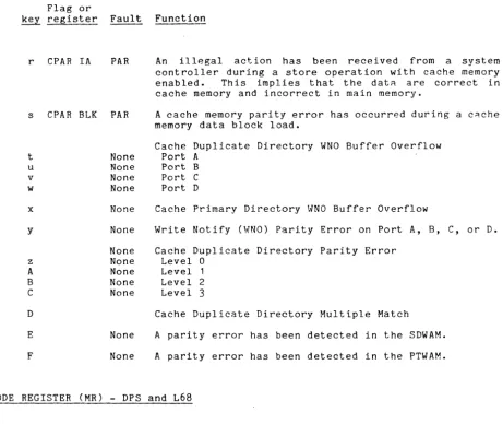
Segment Descriptor Word Associative Memory (SDWAM) - DPS/L68 anct DPS 8M • • • ~ . Page Table Word Associative Memory (PTWAM)
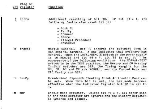
-DPS/L68 and DPS 8M • • • . • • • Fault Register (FR) - DPS/L68 Fault Register (FR) - DPS 8M • • • Mode Register (MR) - DPS and L68 • Mode Register (MR) - DPS 8M • • • Cache ~ode Register (CMR) - DPS and L68 Cache Mode Register (CMR) - DPS 8M • ~ • • • Control Unit (CU) History Registers - DPS
and L68 • • • • • • • • • • • • • • • • • • Control Unit (CU) History Registers - DPS 8M Operations Unit (OU) History Registers . • • Decimal Unit (DU) History Registers - DPS
and L68 • • • • • • • • • • . • • • • . . • Decimal/Operations Unit (DU/OU) History
Registers - DPS 8M • • • . • • • • • . Appending Unit (APU) History Registers - DPS
and L68 • • • • • • • • • • • • • • • . Appending Unit (APU) History Registers - DPS
8M • • • • • • • • . • • • • • • • • • Configuration Switch Data - DPS and L68 Configuration Switch Data - DPS 8M • • Control Unit Data
Decimal Unit Data
Machine Instructions
Instruction Repertoire • •
Arrangement of Instructions • .
Basic Operations • • • • • • • • • • Extended Instruction Set (eis) Operations
EIS Single-Word Operations • • • • EIS Multiword Operations . • • • Format of Instruction Description • • • • • Definitions of Notation and Symbols
Main Memory Addresses • • • • • Index Values • • • • • • • • • Abbreviations and Symbols • • • Register Positions and Contents • • Other Symbols • • • • • • • • • • • Common Attributes of Instructions
Illegal Modification Pari ty Indicator • • • •
Instruction Word Formats • • • • • • • • • . Basic and EIS Single-Word Instructions Indirect Words • • • • • • • •
EIS Multiword Instructions EIS Modification Fields (MF)
MF Coding Examples • • • • • EIS Operand Descriptors and Indirect
Pointers • • • • • • • • • • • • • • Operand Descriptor Indirect Pointer
Format • • • • • • • • • • • . • • • Alphanumeric Operand Descriptor Format Numeric Operand Descriptor Format Bit-string Operand Descriptor Format • Fixed-point Arithmetic Instructions • • • •
Fixed-Point Data Movement Load Fixed-Point Data Movement Store • Fixed-Point Data Movement Shift • Fixed-Point Addition • • • •
CONTENTS (cont)
FixeQ-Point Negate Fixed-Point Comparison Fixed-Point Miscellaneous Boolean Operation Instructions
Boolean AND • • •
Boolean Or • • • • • • • Boolean Exclusive Or Boolean Comparative And •
Boolean Comp~rative Not • . • • • Floating-Point Arithmetic Instructions •
Floating-Point Data Movement Load • • Floating-Point Data Movement Store Floating-Point Addition • • • Floating-Point Subtraction
Floating-Point Multiplication • • Floating-Point Division •
Floating-Point Negate • • Floating-Point Normalize Floating-Point Round
Floating-Point Compare • • • • Floating-Point Miscellaneous • • • . Transfer Instructions • • • • •
Pointer Register Instructions • • • • . Pointer Register Data Movement Load • Pointer Register Data Movement Store Pointer Register Address Arithmetic • Pointer Register Miscellaneous
Miscellaneous Instructions • Calendar Clock
Derail • • • • Execute • • • • • • Master Mode Entry •
No Operation • • • • Repeat • • • • • • • • • • • R in g A I arm Reg i s t e r • • • • • • • Store Base Address Register • • • • • Translation • • • • • • • • • • • • . Register Load • • • • • • • • • . • • . Privileged Instructions • • • • • • • •
Privileged - Register Load
Privileged - Register Store • • • • • Privileged - Clear Associative Memory • • Privileged - Configuration and Status • • Privileged - System Control •
Privileged - Miscellaneous • • • • Extended Instruction Set (EIS) •
EIS - Address Register Load • EIS - Address Register Store
EIS - Address Register Special Arithmetic EIS - Alphanumeric Compare
EIS - Alphanumeric Move • • • • • • . EIS - Numeric Compare • • • • • • EIS - Numeric Hove • • • • • • • • • EIS - Bi t String Combine • • • • • EIS - Bit String Compare • • • • EIS - Bit String Set Indicators • • EIS - Data Conversion • • • • • • • • EIS - Decimal Addition • • • • • • • EIS - Decimal Subtraction • •
EIS - Decimal Multiplication
EIS - Decimal Division • • • • Micro Operations For Edit Instructions
Micro Operation Sequence • • • • • • Edit Insertion Table • • • • •
Section 5
Section 6
I
Section 7
CONTENTS (cont)
Terminating Micro Operations . • • • MVNE and MVE Differences • • • • •
Numeric Edit • • • Alphanumeric Edit Micro Operations
Micro Operation Code Assignment Map •
Addressing -- Segmentation And Paging • Addressing Modes • • • .
Absolute Mode • • • • • • • • • • • . Append Mode • • • • •
Segmentation • • • • • • • • • • • • Paging • • • • • . • • • . • • • • Changing Addressing Modes • • • •
Address Appending • • • • • • • • • . Address Appending Sequences • • • • • Appending Unit Data Word Formats •
Page Table Word (ptw) Format
Virtual Address Formation • • • • • •
Definition of Virtual Address • • • • • Types of Virtual Address Formation
Symbology (aIm) • • • • • •
Symbolic Fields • • • • • • • • • AIm Pseudo-Instructions • • • • • Computed Address Formation • • • •
The Address Modifier (TAG) Field • • • • General Types of Computed Address
Modification • • • • • • • • • • Computed Address Formation Flowcharts Register (r) Modification • • • • • • Examples: • • • • • • . • • • • • • • Register Then Indirect (ri) Modifications
Examples: • . • • • • • • • • • • • Indirect Then Register (ir) Modification
Examples: • • • • • • • • • • • Indirect Then Tally (it) Modification Special Address Modifiers
Indirect to Pointer (ITP) Modification • • • • • • • Indirect to Segment (ITS)
Modification • • • • • • • • Effective Segment Number Generation • Virtual Address Formation for Extended
Instruction Set • • • • • • • • • • • • Character- and Bit-String Addressing Character- and Bit-String Address
Arithmetic Algorithms • • • • • • • 9-bit Byte String Address Arithmetic • 6-bit Character String Address
Arithmetic • • • • • • • • • • • • • 4-bit Byte String Address Arithmetic • Bit String Address Arithmetic
Faults And Interrupts. Fault Cycle Sequence Fault Priority • • Fault Recognition Fault Descriptions
Group 1 Faults Group 2 Faults Group 3 Faults
Section 8
Section 9
Appendix A
Appendix B
Appendix C
Index
Figure 2-1-Figure 2-2. Figure 2-3. Figure 2-4. Figure 2-5. Figure 2-6. Figure 2-7.
Figure 2-8.
Figure 2-9.
Figure 3-1-Figure 3-2. Figure 3-3. Figure 3-4. Figure 3-5.
Figure 3-6. Figure 3-7. Figure 3-8. Figure 3-9. Figure 3-10. F igu('i~ 3 -11 • Figure 3-12.
CONTENTS (cont)
Group 7 Faults • • • • • • Interrupts and External Faults •
Interrupt Sampling • • • • Interrupt Cycle Sequence • • • •
Hardware Ring Implementation Ring Protection in Multics • Ring Protection in the Processor
Appending Unit Operation with Ring Mechanism
Cache Memory Operation • • • • • Philosophy of Cache Memory • •
Cache Memory Organization • • • • • Cache Memory/Main Memory Mapping Cache Memory Addressing • • • • • • Cache Memory Control • • • • • • • •
Enabling ann Disabling Cache Memoryy • • • Cache Memory Control in Segment
Descriptor Words • • • • •
Loading the Cache Memory • • • • Clearing the Cache Memory •
General Clear • • • • • Selective Clear • • • •
Dumping the Cache Memory • • • •
Operation Code Map
Alphabetic Operation Code List
Address Modifiers • • • • • • • • Nonstandard Modifiers
ILLUSTRATIONS
Unstructured Machine Word Format Unstructured Word Pair Format
·
·
Unstructured 4-bit Byte Format Unstructured 6-bit Character Format Unstructured 9-bit Byte FormatUnstructured 18-bit Half Word Format
Eighteen-bit Half Word Floating-Point Binary Operand Format
·
·
·
·
·
· · ·
· ·
·
.
Single-Precision Floating-Point Binary OperandFormat
· · ·
·
· · ·
·
·
· · ·
..
· ·
·
·
·
.
Double-Precision Floating-Point Binary OperandFormat
· ·
·
·
·
· ·
·
· ·
·
·
Accumulator Register (A) Format
· ·
· · ·
·
Quotient Register (Q) Format· · ·
·
· ·
·
Accumulator-Quotient Register (AQ) Format·
Exponent Register (E) Format· ·
· · ·
· ·
Exponent-Accumulator-Quotient Register (EAQ)Format
·
·
·
· ·
·
·
· ·
· ·
·
·
Index Register (Xn) Format·
Indicator Register (IR) Format Base Address Register (BAR) Format Timer Register (TR) Format· ·
·
Ring Alarm Register (RALR) Format·
Pointer Register (PRn) Format· · ·
Address Register (ARn) Format· · ·
Figure 3-14. Figure 3-15. Figure 3-16.
Figure 3-17.
Figure 3-18. Figure 3-19. Figure 3-20. Figure 3-21. Figure 3-22. Figure 3-23. Figure 3-24.
Figure 3-25.
Figure 3-26. Figure 3-27.
Figure 3-28.
Figure 3-29.
Figure 3-30. Figure 3-31. Figure 3-32. Figure 3-33. Figure 4-1. Figure 4-2. Figure 4-3. Figure 4-4. Figure 4-5. Figure 4-6. Figure 4-7. Figure 4-8. Figure 4-9. Figure 4-10. Figure 4-11. Figure 4-12.
Figure 4-13.
Figure 4-14.
Figure 4-15.
Figure 4-16.
Figure 4-17.
Figure 4-18.
Figure 4-19.
Figure 4-20.
Figure 4-21.
Figure 4-22.
Figure 4-23.
Figure 4-24.
CONTENTS (cont)
Temporary Pointer Register (TPR) FormRt • • • • Descriptor Segment Base Register (DSBR) Format Segment Descriptor Word Associative Memory
(SDWAM) Format DPS/L68 and DPS 8M • • • • Page Table Word Associative Memory (PTWAM)
Format DPS/L68 and DPS 8H • • • • • • • • Fault Register (FR) Format - DPS and L68 • Fault Register (FR) Format - DPS 8M • • • • Mode Register (MR) Format - DPS and Lo8 • • Mode Register (MR) Format - DPS 8M • • • • • • Cache Mode Register (CMR) Format - DPS and L68 Cache Mode Register (C~R) Format - DPS 8M • Control Unit (CU) History Register Format - DPS
and L68 • • • • • • • • • • • • • • • • • Control Unit (CU) History Register Format - DPS
8M • • • • • • • • • • • • • • • • • • • •
Operations Unit (OU) History Register Format Decimal/Operations (DU/OU) History Register
Format - DPS 8M • • • • • • • • • • • • • • • Appending Unit (APU) History Register Format
-DPS and L68 • • • • • • • • • • • • • • • • • Appending Unit (APU) History Register Format
-DPS 8M • • • • • • • • • • • • •
Configuration Switch Data Formats - DPS and L68 Configuration Switch Data Formats - DPS 8M Control Unit Data Format • • • • • • Decimal Unit Data Format • • • • • •
Basic and EIS Single-Word Instruction Format Indirect Word Format • • • • • •
EIS Multiword Instruction Format • • • • • EIS Modification Field (MF) Format • • • • Operand Descriptor Indirect Pointer Format Alphanumeric Operand Descriptor Format
Numeric Operand "Descriptor Format • • • • • • • Bit String Operand Descriptor Format
Repeat Double (rpd) Instruction Word Format • • Repeat Link (rpl) Instruction Word Format. Repeat (rpt) Instruction Word Format • • • • • EIS Address Register Special Arithmetic
Instruction Format • • • • • • • • • • • • • • Compare Alphanumeric Character Strings (cmpc)
EIS Multiword Instruction Format • • • • • • • Scan Characters Double (scd) EIS Multiword
Instruction Format • • • • • • • • • • • • • • Scan with Mask (scm) EIS Multiword Instruction
Format • • • • • • • • • • • • • • • • • • Test Character and Translate (tct) EIS
Page 3-15 3-16 3-18 3-20 3-23 3-25 ?--27 3-30 3-32 3-34 3-37 3-39 3-41 3-46 3-49 3-51 3-54 3-56 3-58 3-63 4-7 4-8 It-9 4-9 4-11 • 1 4-12 4-14 4-15 4-145 4-148 4-150 4-183 4-191 4-193 4-196
Mul t iword Instruct ion Format • • • • • • • • • 4-199 Move Alphanumeric Left to Right (mlr) EIS
Multiword Instruction Format • • • • • • • • • 4-202 Move Alphanumeric Edited (mve) EIS Multiword
Instruction Format • • • • • • • • • • • • • • 4-205 Move Alphanumeric with Translation (mvt) EIS
Multiword Instruction Format • • • • • • • • • 4-207 Compare Numeric (cmpn) EIS Multiword
Instruction Format • • • • • • • • • • • • • • 4-210 Move Numeric (mvn) EIS Multiword Instruction
Format • • • • • • Move Numeric Edited Instruction Format Combine Bit Strings Instruction Format Compare Bit Strings
(mvne) EIS Multiword
Left (csl) EIS Multiword
(cmpb) EIS Multiword
4-213
4-216
CONTENTS (cont)
Pap;e
Figure 4-25. Binary to Decimal Convert (BTD) EIS f-1ul t iword
Instruction Format
·
·
·
· · · ·
·
·
4-22h Figure 4-26. Decimal to Binary Convert (dtb) EIS ~1ul tiwordInstruction Format
·
·
·
4-228 Figure 4-21. Add Using Two Decimal Operands (ad2d) EISMultiword Instruction Format
·
· ·
·
· ·
·
4-230 Figure 4-28. Add Using Three Decimal Operands (ad3d) EISMultiword Instruction Format
·
· · · ·
· · ·
·
4-233 Figure 4-29. Micro Operation (MOP) Character Format 4-246 Figure 5-1. Main Memory Address Generation for UnpagedSegments
·
·
·
·
·
·
·
· ·
·
· ·
·
· ·
·
5-3 Figure 5-2. Page Numbp.r Formation·
·
·
·
·
·
·
· · · ·
5-3 Figure 5-3. Main Memory Address Generation for PagedSegments
·
·
·
· ·
· ·
·
·
·
·
·
·
·
5-5 Figure 5-4. Appending Unit Operation Flowchart 5-8 Figure 5-5. Segment Descriptor Word (SOlo/) Format· ·
·
· ·
5-9 Figure 5-6. Page Table Word (PTW) Format· ·
·
·
5-10 Figure 6-1. Address Hodifier (TAG) Field Format·
6-3 Figure 6-2. Common Computed Address Formation Flowchart 6-6 Figure 6-3. Register Modification Flowchart·
·
· ·
· ·
6-1 Figure 6-4. Register Then Indirect Modification Flowchart·
6-9 Figure 6-5. Indirect Then Register Modification Flowchart·
6-11 Figure 6-6. Indirect Then Tally Modification Flowchart 6-18 Figure 6-1. Format of Instruction Word ADDRESS When Bit 29=
1· · ·
·
· ·
· · · ·
6-19Figure 6-8. ITP Pointer Pair Format
·
· · ·
·
·
6-21I
Figure 6-9. ITS Pointer Pair Format·
· ·
· · ·
6-22Figure 6-10. Effective Segment Generation Flowchart
·
· · ·
6-23 Figure 6-11 • EIS Virtual Address Formation Flowchart·
6-25 Figure 8-1. Complete Appending Unit Operation Flowchart 8-4 Figure 9-1. Main Memory/Cache Memory Mapping· ·
·
·
9-3 Figure A-1. Processor Operation Code Map A-2 Figure A-2. EIS MF Codes· ·
· ·
·
·
· ·
·
·
· ·
·
·
A-4TABLES
Table 2-1. Fixed-Point Binary Integer Values
· ·
2-5 Table 2-2. Fixed-Point Binary Fraction Values· · ·
·
2-6 Table 2-3. Floating-Point Binary Operand Values 2-9 Table 2-4. Decimal Sign Character Interpretation·
2-10 Table 2-5. Decimal Data Values· ·
·
·
·
·
·
·
·
· ·
·
2-11 Table 2-6. Character String Data Length Limits· ·
2-12 Table 3-1. Processor Registers· · ·
·
·
·
·
· · ·
·
·
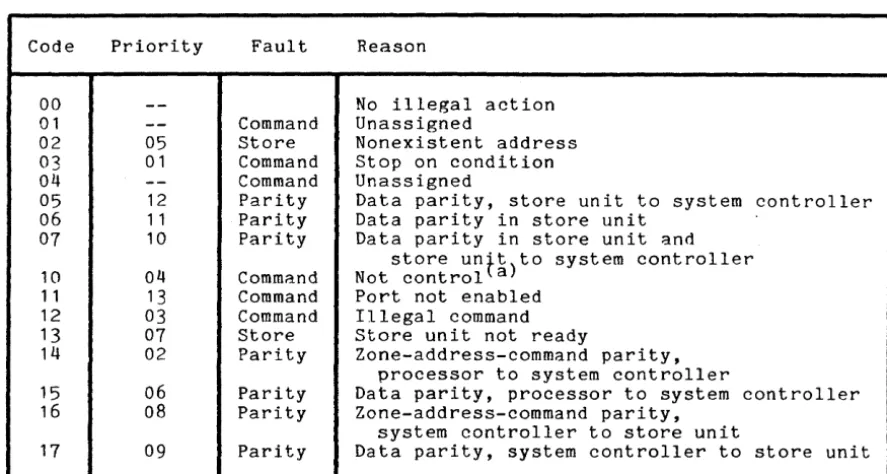
3-1 Table 3-2. System Controller Illegal Action Codes· ·
·
·
3-25 Table 4-1. R-type Modifiers for REG Fields· · · ·
4-10 Table 4-2. Alphanumeric Character Number (CN) Codes 4-13 Table 4-3. Alphanumeric Data Type (TA) Codes· · ·
·
·
·
·
4-13 Table 4-4. Sign and Decimal Type (S) Codes·
· ·
· ·
·
4-14 Table 4-5. Relation Between Data Bits and Indicators·
4-22 Table 4-6. Control Relations for Store Byte Instructions(9-Bit)
·
· · · ·
·
· · ·
·
·
·
4-28 Table 4-1. Control Relations for Store CharacterInstructions (6-Bit)
· ·
· ·
·
4-31 Table 4-8. Default Edit Insertion Table Characters· ·
4-241 Table 4-9. Micro Operation Code Assignment Map·
4-251 Table 5-1. Appending Unit Cycle Definitions 5-1 Table 6-1. General Computed Address ~fod i fica t ion Types· ·
6-5 Table 6-2. Register Modification Decode 6-8 Table 6-3. Variations of Indirect Then Tally Modification 6-13SECTION 1
INTRODUCTION
The- processor described in this reference manual is a hardware module designed for use wi th Multics. The many distinctive features and functio·ns of Multics are enhanced by the powerful hardware features of the processor. The addressing features, in particular, are designed to permit the Multics software to compute relative and absolute addresses, locate data and programs in the Multics. virtual memory, and retrieve such data and programs as necessary.
MULTICS PROCESSOR FEATURES
The Multics processor contains the following general features:
1. Storage protection to place access.restrictions on specified segments.
2. Capabili ty to interrupt program execution in response to an external signal (e.g., I/O termination) at the end of any even/odd instruction pair (midinstruc-tion interrupts are permi tted for some instructions), to save processor status, and to restore the status at a later time without loss of continuity of the program.
3. Capabili ty to fetch instruction pairs and to buffer two instructions (up to four instructions, depending on certain main memory over lap conditions) including the one currently in execution.
4. Overlapping instruction - execution, address preparation, and
instruction fetch. While an instruct ion is being executed, address preparation for the next operand (or even the operand following it) or the next instruction pair is taking place. The operations unit can be executing instruction N, instruction N+l can be buffered in the operations unit (with its operand buffered in a main memory port), and the control unit can be executing instructions N+2 or N+3 (if such execution does not involve the main memory ~ort or registers of instructions N or N+1) or preparing the address to fetch instructions
N+4 and N+5. This includes the capa·bili ty to detect store
instructions that alter the contents of buffered instructions and the
. abili ty to delay preprocessing of an address using register
modification if the instruction currently in execution changes the register to be used in that modification.
5. Interlacing capability to direct main memory accesses to interlaced system controller modules.
6.
Intermediate storage of address and control inf~rmation in high-speed registers addressable by content (associative memory).7.
Intermediate storage of base address and control information inpointer registers that are loaded by the executing program.
9. . Ability
to
hold recently referenced 'operands and instructions in a high-speed look-aside memory (cache option).Segmentation and Paging
A segment is a collection of data or instructions that is assigned a symbolic ·name and addressedsymboli-cally by the user. Paging is controlled by the system software; the user need not be aware of the existence of pages. US.er-visible address preparation is 'concerned with the calculation of a virtual memory address; the processor hardware completes address preparation by
tran~lating the final virtual memory address into an absolute main memory address. The user may view each of his segments as residing in an independent main memory unit. Each segment has its own origin that can be addressed as location zero. The size of each segment varies without affecting the addressing of the other segments. Each segment can be addressed like a conventional main memory image starting at location zero. Maximum segment size is 262,144 words.
When viewed from the processor, main memory consists of blocks or page frames, each of which has a I ength of "page-si zeit words. The page si ze 'used by Multics is 1024 words. Each frame begins at an absolute address which is zero modulo the page size. Any page of a segment can be placed in any available main memory frame. These pages may be addressed as if they were contiguous, even though they may be in widely scattered absolute locations. Only currently referenced pages need be in main memory. A segment need not be paged, in which case 'the complete segment is located in contiguous words of main memory. In Hultics, all user segments are paged. See Section
5
for additional discussion.Address Modification and Address Appending
Before each main memory access, two major phases of address preparation take place:
1. Address modification by register or indirect word content, if specified -by,the instruction word or indirect word.
2. ·Address a'ppending, in which a virtual memory address is translated into an absolute address to access main memory.
Al though the above two types of mod ification are combined in most operations, they are described separately in Sections 5 and 6. The' address mod ification procedure can go on indefin itely, wi th one type of mod ification leading to repetitions 'of the same type' or to other types of modification prior to a main memory access fo'r an operand.
Faults and Interrupts
The processor detects certain illegal instruction usages, faulty communication with the main memory, programmed faults, certain external events, and arithmetic faults. Many of the processor fault conditions 'are deliberately or inadvertently caused by the software and do not necessarily involve error conditions. The processor communicates with the other system modules (I/O multipl'exers 7 bulk store controllers, and other processors) by setting and
should be some form of transfer, or . the -faul tin~ program will be resumed at the point of interruption. Faults and interrupts are described in Section 7.
Interrupts and certain low-priority faults are recognized only at specific times during the execut"ion of an instruction pair. If, at these times, bit 28 in the instruction word is set ON, the trap is inhibited and program execution continues. The interrupt or fault signal is saved for future recognition and is
reset only when the trap occurs.
-PROCESSOR MODES OF OPERATION
There
are
three modes of main memory addressing (absolute mode, append mode, and BAR mode), and two modes of instruction execution (normal mode andprivileged mode).
Instruction -Execution Modes
NORMAL MODE
Most instructions can be executed in the normal mode. Certain
instructions, classed as privileged, cannot be executed in normal mode. These
are identified in the individual instruction descriptions. An attempt to
execute privileged instructions while in the normal mode results in an illegal procedure fault. The processor executes instructions in normal mode only if it is forming addresses in append mode and the segment descriptor word (SOW) for the executing segment specifies a non-privileged procedure.
PRIVILEGED MODE
In privileged mode, all instructions can be executed. The processor
executes instructions in privileged mode when forming addresses in absolute mode
or
when forming addresses in append mode and the segment descriptor word (SOW) for the segment in execution specifies a privileged procedure and the execution ring is equal to zero. See Sections5
and7
for additional discussion.Addressing Modes
ABSOLUTE MODE
In absolute mode, the final computed address-is treated as the absolute main memory address unl ess the append ing hardware meehan ism is invoked for a particular main memory reference. During instruction fetches, the procedure pointer register is ignored. The-processor enters absolute mode when it is initialized or immediately after a fault or interrupt. It remains in absolute mode until it executes a transfer instruction. whose operand is obtained via explicit use of the appending hardware mechanism.
The appending hardware mechanism may be invoked for an instruction by setting bi\ 29 of the instruction word ON to cause a reference to a properly
loaded pointer register or by the use of indirect-to-segment (its) or
APPEND MODE
The append mode is the most commonly used main memory addressing mode. In append mode the final computed address 1s either combined with the procedure pointer register, or it is combined with one of the eight pointer registers.· If bit 29 of the instruction word contains a 0, then the procedure pointer register is select~d; otherwise, the pointer register given by bits 0-2 of the in struction word is selected.
BAR MODE
In BAR mode, the base address register (BAR) is used. The BAR contains an address. bound and a base address. All computed addresses are relocated by adding the base addr·ess. The relocated address is combined with the procedure pointer register to form the virtual memory address. A program is kept within certain limits by subtracting the unrelocated computed address from the address bound. If the result is zero or negative, the relocated address is out of range, and a store fault occurs.
PROCESSOR UNIT FUNCTIONS
Major functions of each principal logic element are listed below and are described in subsequent sections of this manual.
Appending Unit
Controls data input/output to main memory
Performs main memory selection and interlace
Does address appending
Controls fault recognition
Interfaces with cache
Associative Memory Assembly
This assembly consists of sixteen 51-bit page table word associative memory (PTWAM) registers and sixteen 108-bit segment descriptor word associative memory (SDWAM) registers. These registers are used to hold pointers to most recently used segments (SOWs) and pages (PTWs). This unit reduces the need .for possible multiple main memory accesses before obtaining an absolute main m.emory address of an operarid or instruction.
Control Unit
Performs address modification
Controls mode of operation (privileged, normal, etc.)
Decodes instruction words and indirect words
Performs timer register lo~ding and decrementing Operation Unit
Does fixed- and floating-binary arithmetic
Does shifting and Boolean operations
Decimal Unit
Does decimal arithmetic
SECTION 2
DATA REPRESENTATION
INF~RMATION
ORGANIZATION
The processor, like the rest of the Hultics system, is organized to deal
with information in basic units of 36-bit words.
Other units of 4-, 6-, 9-bit
characters or bytes, 18-bit half words, and 72-bit word pairs can be manipulated
wi thin the processor' by use of the instruction set.
These bit groupings are'
used ·by the hardware and software to represent a variety of forms of coded data.
Certain processor
tuncti~nsappear to manipulate larger units of 144, 288, 576,
and 1152 bits, but these functions are performed by means of repeated use of
72-bi t word pairs.
All information is transmitted, stored, and processed as
strings of binary bits.
The data values are derived when the bit strings are
interpreted according to the various formats discussed in this section.
POSITION NUMBERING
The numbering of bit positions, character and byte positions, and words
increases from 0 in the direction of conventional reading and writing: from the
most significant to the least significant digit of a number, and from left to
right in conventional alphanumeric text.
Graphic presentations in this manual show registers and data with position
numbers increasing from left to right.
NUMBER SYSTEM
The binary arithmetic functions of the processor are implemented in the
twos compl·ement, binary number system.
One of the primary properties of this
number
system is that a field (or register) having width. n bits may be
interpreted in two different ways; the logical case and the- ari thmetic or
algebraic case.
In the logical case, the number is unsigned, positive, and lies in the
range
[0,2.!!.-1] where- n is the size of the register or the length of the field.
I
The results of arithmetic operations on numbers for this case are interpreted as
modulo
2~numbers.
OverflOW is not defined for this case since the range of the
I
field or register cannot be exceeded.
The numbers
0and 2'!!'-' are consecutive
(not separated) in the set of numbers defined for the field or register.
Iq the arithmetic case, the number is signed and lies in the range
[-2(.!!.- >,2(!1-1 )-1].
Overflow is defined for this case since the range can be
exceeded in either direction (positive or negative).
The left-hand-most bit of
the field or register (bit
0)serves as the sign bit and does not contribute to
The main advantage of this implementation is that the hardware arithmetic algorithms for the two cases are identical; the only distinction lying in the
interpretation of the results by the user. Instruction set features are
provided for performing binary arithmetic with overflow disabled (the so-called logical 'instructions) and for comparing numbers in either sense.
Subtraction is performed by add,ing the twos complement of the subtrahend to the minuend. (Note that when the subt·r.ahend is zero the algorithm for forming the twos complement is still carried out, but, since the' twos complement of zero is zero, the result is correct.)
Another important feature of the twos comp'lement number system ,( wi th respect to comparison of numeric values) is that the no borrow condition in true subt'racti.on is identical
to
the carry condition in true addition and vice versa.A statement on the assumed location of the binary point' has significance only for multiplication and division. These two operations are implemented for the arithmetic case in both integer and fraction modes. Integer means that the posi tion of the binary 'point is assumed to the right of the least significant bit position, that Is, to the right of the right-hand-most bit of tile field or register, and fraction means that the posi tion of the binary point is assumed
to
the left of the most significant bit position, that is, between bit 0 and bit 1 of the field or register (recall that bit 0 is the sig'n bit).
INFORMATION FORMATS
The figures that follow show the unstructured formats (templates) for the various information units defined for the processor. Data transfer between the processor and main memory is word oriented; a 36-bit machine word is transferred for single-precision operands and subfields of machine words, and a 72-bit word
pair is transferred for all other cases (multiword operands, instruction
fetches, bit- and character-string operands, etc.). The information unit to be used and the data transfer mode are determined by the processor according to the function to be performed.
The 36-bi t unstructured machine word shown in Figure 2-1 is the mln lmum
addressable information unit in main memory. Its location is uniquely
determined· by its main memory address, Y. All other information units are defined relative to the 36-bit machine word.
Figure 2-1. Unstructured Machine Word Format
Two consecuti ve machine words as shown in Figure 2-2, the fir st hav ing an even main memory address, form a,72-bit word pair. In 72-bit word pair data transfer mode" the word pair is uniquely located by the main memory address of either of its constituent 36-bit machine words. Thus, if Y is even, the word pair at (Y,Y.l) is selected. If Y is odd, the word pair at (Y-1,Y) is selected.
o
3 3
7Even word
Odd word
Figure 2-2.
Unstructured Word Pair Format
Four-bit bytes are mapped onto 36-bit machine words as shown in Figure 2-3.
The 0 bits at bit positions 0,
9, 18, and 27 are forced to be 0 by the processor
on data transfer"s to main memory and are ignored on data transfer s from main
memory.
o
0o
0 001 1 1 11 12 2
2 2 2
3 3
3
o
141~
§I!I
Q
3
1
4
II:I~
~r
6
1
!,a
l(
~H
1
1 11 11 1 11 11 1 11
4
14
4
Figure 2-3. Unstructured 4-bit Byte Format
Six-bit characters
ar~mapped onto 36-bit machine words as shown in Figure
2-4.
0
o
0 1 1 1 "12 2
2 3
3
0
:r
12
:r
:(
:(
:1
I
6
I
Figure 2-4.
Unstructured
6~bitCharacter Format
Nine-bit bytes are mapped onto 36-bit machine words as shown in Figure 2-5.
0
o
0 1 12 2
3
f
§I~
II§
6
1
I
~1
9 9 9 9
Figure
2-5~Unstructured 9-bit Byte Format
0
1 1 3I
Q
Zi
a
~I
18 18
Upper naIf Lower nalf
Figure 2-6. Unstructured 18-bit Half Word Format
DATA PARITY
Odd parity on each 36-bi t machine word transferred to main memory is generated as it leaves the processor, is verified at several points along the transmission path, and is held in main memory either as an extra bit in the case of magnetic core memory or as part of the error detecting and correcting (EDAC) code in the case of magnetic oxide semiconductor (MOS) memory. If an incorrect pari ty is detected at any of the various parity check points, the main memory r.eturns an illegal action signal and a code appropriate to the cneck pOint.
On data transfers from main memory, the parity information is retrieved and transmi tted wi th the data information. The same ver.ification checks are made and illegal action signalled for errors. The processor makes a final parity check as the data enters the processor.
Any detected parity error c-auses the processor parity indicator to be set ON and (if enabled) a parity fault occurs.
REPRESENTATION OF DATA
Data is defined by imposing an operand structure on the information units just described.- Data is represented in two forms: numeric or alphanumeric. The form is determined by the processor according to function to be performed.
In the definitions below, a
i is - the value of the bit in the i th bit position, either 0 or 1.
Numeric Data
Numeric data is represented in three modes: - fixed-point binary,
floating-point binary, and decimal. The mode is determined by the processor according to the function being performed.
FIXED-POINT BINARY DATA
Fixed-Point Binary Integers
[image:21.617.52.556.467.675.2]Logical value:
aox2(~-1) + a1 x2 (n-2) + ••• + aix2(~-i-1) + ••• + a n_l Arithmetic value:
-aox2(~-1) + alx2(~-2) + ••• + aix2(~-i-l) + ••• + an_1
The following fixed-point binary integer data items are defined (also see Table 2-1 for values):
Operand size(bits)
6
9
18 36 72
Operand name
6-bit character operand 9-bit byte operand Half word operand
Single-precision operand Double-precision operand
Note that a 4-bit operand is not defined. This data item is defined only for decimal data. (See discussion of decimal data later in this section).
The proper operand and its position with respect to a 36-bit machine word are determined by the processor during preparation of the main memory address for the operand. If the data width of the operand selected is smaller than the register involved, the operand is high- or low-order zero filled as necessary.
The values in Table 2-1 are given in terms of the operand sizes. The value an operand contributes to a larger field or register depends on the alignment of the operand with respect to the field or register.
Table 2-1. Fixed-Point Binary Integer Values
36-bit 72-bit
Operand 6-bit 9-bit 18-bit single double
character byte half word precision precision
Logical
minimum 0 0
2 18_1 23R_1
27~_1
maximum 26_1 29 -1
resolution 1 1 1 1 1
Arithmetic
minimum 0 0 0 0 0
maxima
_25 _2 8 17 _§35 71
negative
2i~_1
21~-1
positive 25 _1 28_1 2 3 '-1
resolution 1 1 1 1 1
Fixed-point Binary Fractions
r ixed-point binary fraction data is defined by imposing the bit position value expression below on an information unit of ~ bits.
I
Arithmetic value:
a x2 -1 2-2 2- i 2-(n-l) -aO + 1 + a2 x + ••• + ai x •.. + a n _l x
-Note that logical values are not defined for fixed-point binary fraction data.
The following fixed-point binary fraction data items are defined (also see Table 2-2 for values): .
Operand
size(bits) Operand name
6-bit character operand 9-bit byte operand Half word operand
Single-precision operand Double-precision operand
Note that a 4-bit operand is not defined. This data item is defined only for decimal data. (See discussion of decimal data- later in this section.) Fixed-point binary fract(on operands are used by the Divide Fraction (dvf) and Multiply Fraction (ropf) instructions only.
The proper operand and its position with respect to a 36-bit machine word are determined by the processor during preparation of the main memory address for the operand. If the data width of the operand selected is smaller than the register involved, the operand is high- or low-order zero filled as necessary.
The values in Table 2-2 are given in terms of the operand sizes. The value an operand contributes to a larger field or register depends on the alignment of the operand with respect to the field or register.
Table 2-2. Fixed-Point Binary Fraction Values
36-bit 12-bit Operand 6-bit 9-bit 18-bit single double
character byte half word precision precision
Arithmetic
minimum 0 0 0 0
a
maxima
negative -1.0 -1.0 -1.0 -1.0 -1.0
positive 1.0-§-5 1.0-~-8 1.0_~-11 1.0_~-35 1.0-
7-
11resolution 2- 2- 2- 1 . 2- 5 2- 1
FLOATING-POINT BINARY DATA
where:
M is a fixed-point binary fraction; the mantissa
E is a fixed-point binary integer; the exponent
A floating-point binary number is defined by partitioning an information unit of n bits into two pieces; an 8-bit fixed-point binary integer exponent and an (~-8)=bit fixed-point binary fraction mantissa.
The following floating-point data items are defined.
Operand size(bits)
18
36
72
Operand name
Half word operand
Single-precision operand Double-precision operand
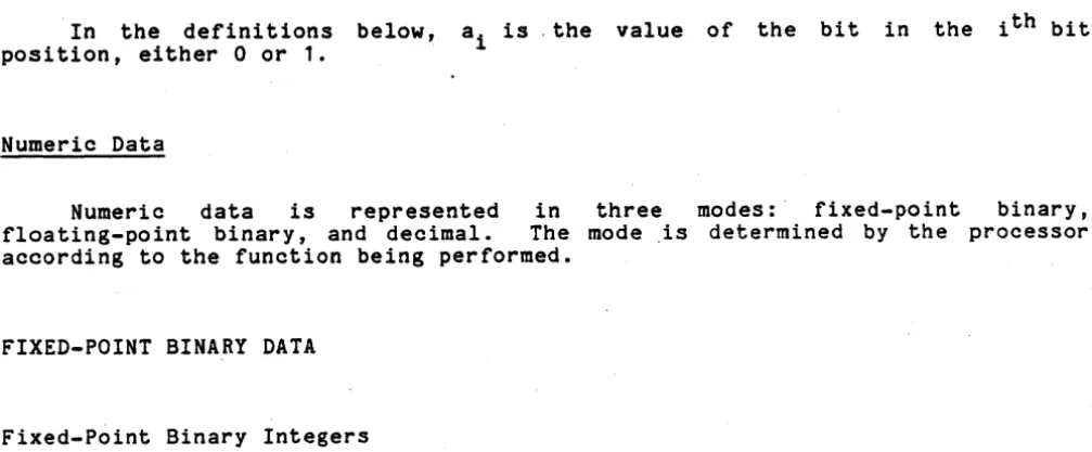
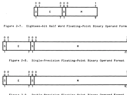
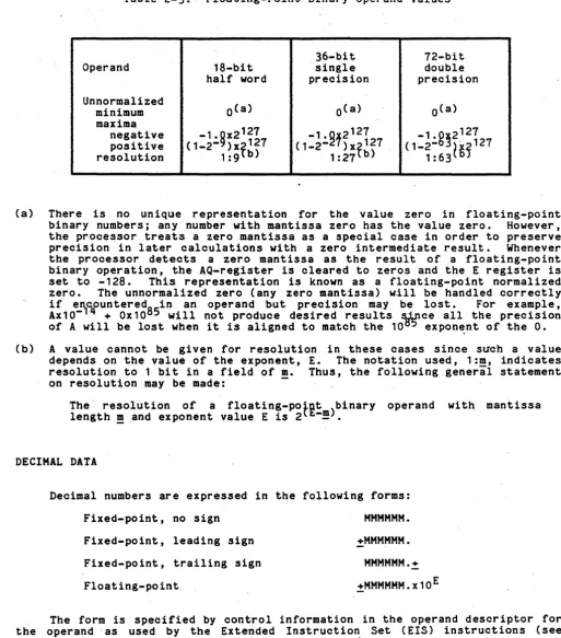
For clarity, the formats of these operands are shown in Figure 2-7 through Figure 2-9. In the figures, the fields labeled S hold sign bits associated with the exponent, E, and the mantissa, M.
The floating-point binary operands are used only by the floating-point binary arithmetic instructions (see Section 4). The 18-bit half word operand has meaning only when used in conjunction with the direct upper (du) address modification (see Section 6 for a discussion of address modification).
o
0 0 0 0E M
7 1 9
Figure 2-7. Eighteen-bit Half Word Floating-Point Binary Operand Format
o
0 0 0 0 3o
1lsi
E M7 27
Figure 2-8. Single-Precision Floating-Point Binary Operand Format
o
0 0 0 0 7o
1lsi
E M7
Figure 2-9. Double-Precision Floating-Point Binary Operand Format
[image:24.620.119.542.417.736.2]The proper operand is selected by the processor during preparation of the main memory address for the operand.
Overlength Registers
The AQ-register is used to hold the mantissa of all floating-point bin~ry
numbers. The AQ-register is said to be overlength with respect to the operands since it has more bits than are provided by the operands. Operands are low-order zero filled when loaded and low-order truncated (or rounded, depending on the instruction) when stored. Thus, the result of all floating-point instructions has more bits of precision in the AQ-register than may be store~.
Users are cautioned that calculations involving floating-point operands may suffer from propagation of truncation errors even if the computation algorithms are designed to hold mantissas in the AQ-register as long as possible. It is possible to retain full AQ-register precision of intermediate resul ts if they are saved with the Store AQ (staq) and Store Exponent (ste) instructions but such saved data are not usable as a floating-point operand.
Normalized Numbers
A floating-point binary number is said to be normalized if the relation
I
-0.5>
M>
- l o r 0.5 ~ M <lor [M=O and E=-128]I
is satisfied. This is a result of using a 2's complement mantissa. Bits 8 and 9 are different unless the number is zero. The presence of unnormalized numbers in any finite mantissa arithmetic can only degrade the accuracy of results. For examPle'2in an arithmetic allowing only two digits in the mantissa, the number 0.005x10 has the value zero instead of the value one-halfNormalization is a process of shifting the mantissa and adjusting the exponent until the relation above is satisfied. Normalization may be used to recover some or all of the extra bits of the overlength AQ-register after a floating-point operation.
There are cases where the limits of the registers force the use of unnormalized numbers. For example, in an arithmetic allowinf three digi
y
1
of mantissa and one digit of exponent, the calcul~tion 0.3x10- 0 - 0.lx10- (the normalized case) may not be made, but 0.03x10- - 0.OOlx10- 9 = 0.029x10- 9 (the unnormalized case) is a valid result.are:
Some examples of normalized and unnormalized floating-point binary numbers
Unnormalized positive binary 0.00011010 x 27
Same number normalized 0.11010000 x 24
Unnormalized negative binary 1.11010111 x 2- 4
Same number normalized 1.01011100 x 2-6
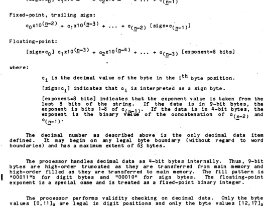
Table 2-3.
Floating-Po.int Binary Operand ·Values
36-bit
72-bit
Operand
18-bit
single
double
half word
precision
precision
Unnormalized
O(a)
O(a)
O(a)
minimum
maxima
-1.
ijX2-127
1
9~2127 _1.g~2127negative
positive
(1-2- ) xf 127
(1:2':'
) xf 127
(1;..2-
~~~127resolution
1:9
b) 1:27
b)1:63
(a)
There is no unique representation for the value zero in floating-point
binary numbers; any number with mantissa zero has the value zero.
However,
the processor treats a zero mantissa as a special case in order to preserve
precision in later calculations with a zero intermediate result.
Whenever
the processor detects a zero mantissa as the result of a floating-point
binary operation, the AQ-register is cleared to zeros and the E register is
set to -128.
This representation is known as a floating-point normalized
zero.
The unnormalized zero (any zero mantissa) will be handled correctly
if
en1~ountered85inan operand but precision may be lost.
For example,
Ax10-
+ Ox10
will not produce desired results
~ceall the precision
of A will be lost when it is aligned to match the 10
expon~ntof the O.
(b)
A value cannot be given for resolution in these cases since such a value
depends on the value of the exponent,
E.
The notation used, 1:m, indicates
resolution to 1 bit in a field of m.
Thus, the following generil statement
on resolution may be made:
-The· resolution of a floating-potRt )binar y operand with mantissa
length
!! _and exponent value E is 2
-!!.DECIMAL DATA
Decimal numbers are expressed in the following forms:
Fixed-point, no sign
MMMMMM.
Fixed-point, leading sign
+MMMMMM.
Fixed-point, trailing sign
MMMMMM.+
Floating-point.
+HMMMMM.x10 E
The form is specified by control information in the
op~randdescriptor for
the operand -as used by the Extended Instruction Set (EIS) instructions (see
Section
~for a discussion of the EIS instructions).
A decimal number is defined -by imposing any of the byte position value
expressions below on a 4- or 9-bit byte information unit of length n bytes.
Fixed-point, no sign:
[image:26.615.49.562.36.619.2]I
Fixed-point, -leading sign:
[sign:c
O] c1x10(~-2) + c2x10(~-3) + • •• + Fixed-point, trailing sign:
cOX10(~-2).+ C1x10(~-3)
+ ••• +CC~-2) [sign:C(~_1)]
Floating-po in t:
[sign:cO] c1xl0(~-3) + C2x10(,!!-4) + ••• + C(,!!_3) [exponent:8 bits] where:
c i is the decimal value of the byte in the ith byte position. [sign:ci ] indicates that ci is interpreted as a sign byte.
[exponent:8 bits] indicates that the exponent value is taken from the last 8 bits of the string. If the data is in 9-bit bytes, the exponent is bits 1-8 of c( 1). If the data is in 4-bit bytes, the exponent is the binary
v~.rue
of the concatenation of c(,!!_2) and cC,!!_l ) •The decimal number as described above is the only decimal data item defined. It may begin on any legal byte boundary (without regard to word boundar ies) and has a max imum extent of 63 bytes.
The processor handles decimal data as 4-bit bytes internally. Thus, 9-bit bytes are high-order truncated as they are transferred from main memory and high-order filled as they are transferred to main memory. The fill pattern is "00011"b for digit bytes and "00010" for - sign bytes. The floating-point exponent is a special case and is treated as a fixed-point binary integer.
The processor performs validity checking on decimal data. Only the byte v al ue s [ 0, 11 ] 8 ar e 1 eg al in d ig it po si ti 0 n san don 1 y the b yt e v al ue s [1 2, 17] 8 are legal in sign positions. Detection of an illegal byte value causes an illegal procedure fault. The interpretation of decimal sign bytes is shown in Table 2-4.
Table 2-4. Decimal Sign Character Interpretation
9-bit 4-bit
bytes bytes In ter pr eta tio n
52 8 12 8 +
53 8 (a) 138(b) +
548 148(a) +
55
8 (a) 158(a)
-568 16 8 +
.
[image:27.621.29.558.49.460.2](a) This value is usp.d as the default sign byte for storage of results. The presence of other values will yield correct results according to the interpretation.
(b) An optional control bit in the EIS decimal arithmetic instructions (see Section 4) allows the selection of 138 for the plus sign byte for storage of results in 4-bit data mode.
Decimal Data Values
The operand descriptors for decimal data operands have a 6-bit fixed-point binary integer field for specification of f'! scaling factor (SF).' This scaling
factor has the same effect as the value of E in floating-point decima] operands; a negative value moves the assumed decimal point to the left; a positive value, to the right. The use of the scaling factor extends the range and resolution of decimrtl datrt operands. The range of the scaling factor is [-32,31] 10. See Table 2-5 for decimal data operand values.
Table 2-5. Decimal Data Values
~ixed-point Fixed-point Floating-point Floating-point
Operand unsigned signed 9-bit 4-bit
Arithmetic
OCa) O(a) O(a)
minimum 0
maximum (10 63 _1)xl0 31 +(10 62 _1)x10 31 +(1061_1)x10158 +(1060_1)x1Q158 1 :SF(b) - 1:SF(b)
-
1:SF+E(c)-
1:SF+E(c) resolution(a) As in floating-point binary arithmetic, there is no unique representation of the value zero except in the case of fixed-point, unsigned data. Therefore, the processor det ects a zero resul t and forces a value of +0. for fixed-point, signed data and +0.x10 12-, for floating-point data. Again, as in floating-point binary arithmetic, other representations of the value zero will be handled correctly except for possible loss of precision during operand alignment.
(b) A value cannot be given for resolution in these cases since such a value depends on the value of the scaling faf~~f' SF. The notation used, l:SF, indicates resolution to 1 part in 10 • Thus, the following general statement on resolution may be made:
The resolution of a fixed-point decimal operand with scaling factor SF is 10SF .
(c) A value cannot be r-iven for resolution in these cases since such a value depends on the values of the scaling factor, SF, and the exppgrn~1 E. The notation used, 1: SF+E, indicates reso1ut ion to 1 part in 10 + • Thus, the following general statement on resolution may be made:
The resolution of a flo~11~-point decimal operand with scaling factor SF and exponent E is 10 + .
Alphanumeric Data
Alphanumeric dat.a is r'epresented in two modes; character-string and bit-string. The mode is determined by the processor according to the function being per formed.
CHARACTER STRING DATA
Character string data is defined by imposing the character position structure below on a 4-bit, 6-bit, or 9-bit information unit of length ~ bytes or characters.
where:
ci is the character in the ith character position.
U
indicates the concatenation operation.The character string described above is the only character string data item defined. It may begin on any legal character boundary (without regard to word boundaries) and has a maximum extent as shown in Table 2-6.
Table 2-6. Character String Data Length Limits
Character si ze
9-bit 6-bit 4-bit
Length limit
1048576 1572864 2097152
No interpretation of the characters is made except as specified for the instruction being executed (see Section 4).
BIT STRING DATA
Bit string data is defined by imposing the bit position structure below on a bit information unit of length n bits.
where:
b i is the value of the bit in the ith position.
The bit string described above is 'the only bit string data item defined.
It may begin at any bit position (without regard to character or word
SECTION 3
PROGRAM ACCESSIBLE REGISTERS
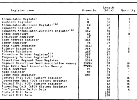
A processor register is a hardware assembly that ho~ds information for use in some specified way. An accessible register is a register whose contents are available to the user for his purposes. Some accessible registers are explicitly addressed by particular instructions, some are implicitly referenced during the course of execution of instructions, and some are used in both ways. The accessible registers are listed in Table 3-1. See Section 4 for a discussion of each instruction to determine the way in which the registers are used.
Table 3-1. Processor Registers
Register name
Accumulator Register Quotient Register
Accumulator-Quotient Register(a) Exponent Register
Exponent-Accumulator-Quotient Register(a) Index Registers
Indicator Register Base Address Register Timer Register
Ring Alarm Register Pointer Registers Address Registers
Procedure Pointer Register«b» Temporary Pointer Register b Descriptor Segment Base Register
Segment Descriptor Word Associative Memory Page Table Word Associative Memory
Fault Register Mode Register
Cache Mode Register
Control Unit (CU) History Register Operations Unit (OU) Bistor'Y Register Decimal Unit (DU) History Register Appending Unit (APU) History Register Configuration Switch Data
Control Unit Data Decimal Unit Data
Mnemonic A Q AQ E EAQ Xn
IR
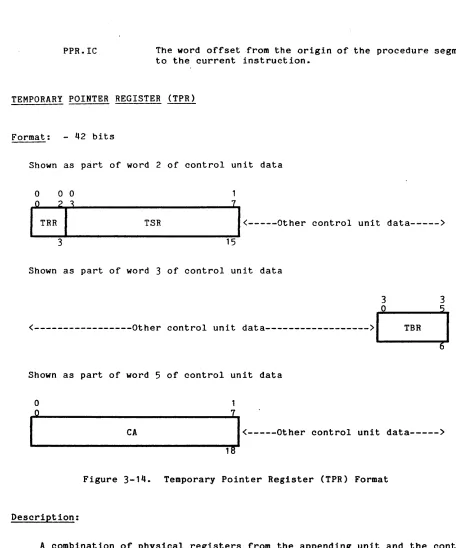
BAR TR RALR PRn ARn PPR TPR DSBR SDWAM PTWAM FR MR CMR Length (bits) 36 36 72 8 80 18 14 18 27 3 42 24 37 42 51 88 51 35 33 28 72 72 72 72 36 288 288 Quantity 1 1 1 1 1 8 1 1 1 1 8 8 1 1 1 16 16 1 1 1 16 16 16 16 5 1 1 [image:32.617.114.563.356.685.2](b) This register is not explicitly addressable, but is included be~ause of its vital role nd DPS 8M"/ p p 980,982P "976,986P in instruction and operand address preparation.
In the descriptions that follow, the diagrams given for register formats do not imply that a physical assembly possessing the pictured bit pattern exists. The diagram is a graphic representation of the form of the register data as it appears in main memory when the register contents are stored or how data bits must be assembled for loading into the register.
If the diagrams contain the characters "x" or "0", the values of the bits in the positions shown are irrelevant to the register. Bits pictured as "x" are not changed when the register is stored. Bits pictured as "0" are set to 0 when the register is stored. Neither "x" bits or
"0"
bits are loaded into the register.ACCUMULATOR REGISTER (A)
Format: - 36 bits
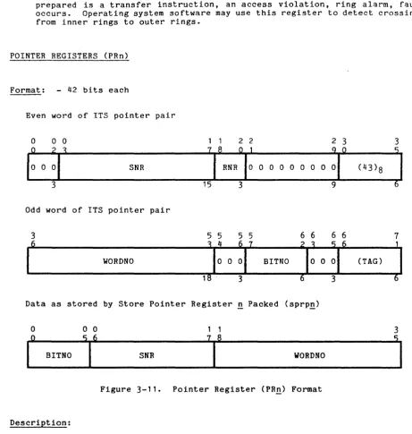
o
1 13
A-Upper A-Lower
Figure 3-1. Accumulator Register (A) Format
Description:
A 36-bit physical register located in the operations unit.
Function:
In fixed-point binary instructions, holds operands and results.
In floating-point binary instructions, holds the most significant part of the mantissa.
In shifting instructions, holds original data and shifted results.
QUOTIENT REGISTER (Q)
Format: - 36 bits
0 1 1 3
Q
1:r
1:
1
I
Q-Upper Q-LowerFigure 3-2. Quotient Register (Q) Format
Description:
A 36-bit physical register located in the operations unit.
Function:
In fixed-point binary instructions, holds operands and results.
In floating-point binary instructions, holds the least significant part of the mantissa.
In shifting instructions, holds original data and shifted results.
In address preparation, may hold two logically independent word offsets, Q-upper and Q-lower, or an extended range bit- or character-string length.
ACCUMULATOR-QUOTIENT REGISTER (AQ)
Format: - 72 bits
o
3 3 7Even Word Odd Word
Figure 3-3. Accumulator-Quotient Register (AQ) Format Description:
Function:
In fixed-point binary instructions, holds double-precision operands and results.
In floating-point binary instructions, holds the mantissa.
In shifting instructions, holds original data and shifted results.
EXPONENT REGISTER (E)
Format: - 8 bits
o
o
o
7 0 8 3 5exponent 0 0 0 0 0 0 0 0 0 0 0 0 0 0 0 0 0 0 0 0 0 0 0 0 0 0 0 0
8 2H
Figure 3-4. Exponent Register (E) Format
Description:
An 8-bit physical register located in the operations unit.
Function:
In floating-point binary instructions, holds the exponent.
EXPONENT-ACCUMULATOR-QUOTIENT REGISTER (EAQ)
Format: - 80 bits
o
o
0 7:1
8
exponent __ mantissa
Figure 3-5. Exponent-Accumulator-Quotient Register (EAQ) Format