Analysis of a Third-Order Charge-Pump Phase-Locked
Loops used for Wireless Sensor Transceiver
ABSTRACT
The evaluation of integrated circuits such as Phase Locked Loops is a challenge in mixed-signal design. In most cases, these circuits are evaluated with electrical stimulations. To verify the proper operation of system before moving on to the design process, it is necessary to model these performances parameters with a hardware description language. At behavioral level, the performances of circuits are optimized without considering its transistor level structure. This paper, present an exact s-domain model analysis of a Third-Order Charge-Pump Phase-Locked Loops (CP-PLLs) used for wireless sensor transceiver using state equations of Phase Frequency Detector. Both the state equations and the transfer functions behavior modeling are described using this analysis. The linear state equations and s-domain transfer functions are provided. Critical advantage of illustrated methodology is a shortened PLL operating process due to the use of fast-simulating models at behavioral level. The analysis is verified using behavioral simulations with VHDL-AMS in Simplorer.
General Terms
Computer Science, Communications.
Keywords
CP-PLLs, State Equations, S-Domain Model, Behavior Modeling, VHDL-AMS.
1.
INTRODUCTION
There are two basic types of transceiver hardware architectures: super heterodyne and direct conversion. A super heterodyne receiver thought to provide high selectivity and sensitivity but it requires several off-chip passive filters such as image-reject filter which make single-chip implementation and low-power receiver design difficult. The direct conversion architecture has been well-recognized for full integration on a single chip. It requires no image-reject filter, and only a RF part.
Fig.1. Wireless Sensor Architecture
Fig.1 presents the different blocks constituting wireless sensor architecture; a complex digital part (DSP) that treats the baseband data and a mixed part (transmission chain) that incorporates the RF section. Generally, a transmission chain consists of a transmitter and one receiver, as well as frequency synthesis part.
The proposed transceiver chain architecture is depicted in Fig.2. Transceiver chain consists of a transmission and a receiver parts. The communication between transmitter and receiver parts is powered through propagation channel. The retrieved signal from the receiver output must be close to the signal input of the transmitter.
Fig.2. Transceiver Chain Diagram Block
The proposed transmitter part architecture is presented in Fig.3. The transmitter section consists of a processing block of the Baseband signal, a Digital Signal Processing unit (DSP), a Modulator, a Mixer which together analog Front End, and a Power Amplifier.
Fig.3. Transmitter Part Architecture
The proposed receiver architecture is shown in Fig.4. It comprises a Low Noise Amplifier, a Demodulator and DSP unit. In reception chain, the RF signal received by the antenna is amplified with a LNA then is converted to a baseband by demodulation function including frequency translation, and decomposition in two signals; I and Q. These two signals are digitally treats by the DSP.
Fig.4. Receiver Part Architecture
The frequency synthesis is obtained by using PLL system. The latter is located in the modulation phase of the transmitter part and in the demodulating phase of the receiver part.
Due to a large number of desirable applications, performance parameters such as the loop bandwidth, damping factor and
Frequency Translation
IF RF
IF-VCO Q
I
DSP Modulator AP
Mixer
RF-VCO
BB Antenna
LNA
Q I
DSP
Demodulator
VCO Antenna
Intissar Toihria
University of Sfax National School of Engineering of Sfax Laboratory of Electronic and
Micro-technology Communication (EMC),
Sfax, Tunisia
Rim Ayadi
University of Sfax National School of Engineering of Sfax Laboratory of Electronic and
Micro-technology Communication (EMC),
Sfax, Tunisia
Mohamed Masmoudi
University of Sfax National School of Engineering of Sfax Laboratory of Electronic and
Micro-technology Communication (EMC),
Sfax, Tunisia
RF Baseband
Controller
Transmitter (Tx)
Receiver (Rx) Propagation
lock range, and design characteristics CP-PLLs systems have in recent years become a popular PLLs architecture. CP-PLLs are widely exploited in diversity applications such as frequency and phase synthesizers, FM and PM demodulators, clock and data recovery systems generate an on-chip clock [1], [2] wireless transceivers, and disk drive electronics [3], [4]. One of the main reasons for the widely adopted use of the CP-PLLs in most PLLs systems is because it provides the theoretical zero static phases offset, and one of the simplest and most effective design platforms.
While there are numerous PPLs design example in the literature, precise and clarity analysis of the loop dynamics of third order CP-PLLs is lacking. The two most popular references in this arena by Hein Scott [5] and Gardner [6] provide useful insight and analysis for a second order PLLs. Other references [7], [8] provide simplified yet useful approximations of third order PLLs. However, they do not provide a complete and extensive analysis for practical integrated circuit PLLs. The majority of IC designers [9], [10] analyze CP-PLLs by treating the PLL loop as a continuous-time system and by using a basic s-domain and z-domain models.
This research focuses on clarify a mathematically exact analysis and insightful understanding of third-order CP-PLLs used for wireless sensor transceiver and accurate transfer functions of a practical CP-PPLs. The rigorous side of this work will expand on Gardner’s work in [6]. In addition, the linearized of the state-space model resulting in the s-domain transfer function is developed. The proposed analysis method based in state equations of PFD.
The outline of this paper is the following. Section 2 briefly presents the basic concept of Third-Order CP- PLLs. The s-domain model analysis of CP-PLLs based state equations of PFD is described in Section 3. Behavioral simulations results using VHDL-AMS in simplorer are presented in section 4. Finally, section 5 draws the concluding remarks of the paper.
2.
CONCEPT OF THRID-ORDER
CP-PLLs
A typical implementation of Charge-Pump Phase-Locked Loops (CP-PLLs) consists of a Phase Frequency Detector (PFD), a Charge Pump (CP), a passive Loop Filter (LF), a Voltage Controlled Oscillator (VCO) and a Divide by N Counter (DBN). A divider is used in feedback; in application requiring clock generates but is omitted in some application for simplicity. The simplified functional block diagram of the third-order CP-PLLs is shown in Fig.5 along with the sequential state diagram of the PFD.
Fig.5. Third-Order CP-PLLs Block Diagram The three states PFD generates Up and Down signals depending on the time (phase) difference between the positive edges of the reference signal and the feedback signal. The CP converts the digital format into analog quantities. This information is filtered by a second-order passive low filter and
converts it to a control voltage and then is used to control the VCO. Thereafter, the frequency oscillation of VCO is divided by DBN counter. For further information on CP-PLLs operation can be found in [11].
2.1
CP Controlled with Three States of PFD
A general structure of CP controlled with three states of PFD circuit is presented in Fig.6 [12] [13].
Fig.6. General Structure of CP Controlled by a PFD The PFD delivers a pair of digital pulse Up and Down corresponding to the phase or frequency error between its input signals which are respectively reference signal and feedback signal; VCO output or DBN output if is used in feedback, in the form of three sequential logic states [6], [14], [15], by comparing the positive (or negative) edges of the tow inputs.
To assure a proper operation of associated Charge Pump to Phase Frequency Detector, an inverter circuit is added to Up signal and a transmission gate circuit is added to Down signal.
is the inverse of the Up and Down maintains its previous states. and Down terminals of PFD are the input signals of Charge Pump circuit.
A Charge Pump generally associated with the Phase Frequency Detector. It is consists of two CMOS switches controlled by the output signals of PFD. Then, it is utilized to convert the sequential logic states of PFD into analog signal [14], [15]. The current generates by CP is proportional to the time difference between the Up and Down pulse.
The traditional PFD is a sequential circuit; it can be represented by a finite state machine consisted of three states. Fig.7 illustrates the state graph of the PFD where is driven by a given type of edges; falling edges or rising edges of and
. In this case, PFD is driven by a rising edges.
Fig.7. Diagram States of CP-PFD
The states of the PFD are represented by digital output signals Up and Down, and can be defined with:
Up=0 ( =1) and Down=1 then charge pump current is negative and equal to - .
Up=0 ( =1) and Down=0 then charge pump current is null.
Up=1 ( =0) and Down=0 then charge pump current is positive and equal to + .
Sref
Sfdb
Sref
Sref
Sfdb
Sfdb
𝑢𝑚 = 0
𝑢𝑚 = - 𝑢𝑚 𝑢𝑚 = + 𝑢𝑚
Up= 0
( =1)
Down=1
Up= 0
( =1)
Down=0
Up= 1
( =0)
Down=0
It is obvious that the Charge Pump is controlled by these states, i. e. by the PFD output signals Up and Down.
2.2
Loop Filter
The used LF is a second order low-pass filter. Its purpose is to convert the charge pump current into a voltage control after it filters the alternating current component. Also, it is used to suppress the noise and high frequency signal components from the CP and to stabilize the loop.
2.3
Voltage Controlled Oscillator
The resulting control voltage drives the VCO; the last generates an oscillation frequency proportional to output voltage [16] of LF circuit.
2.4
Divider by N Counter
The oscillation frequency of VCO is then fed to the divide by N ( = ) which acts as a frequency counter before being fed back to the PFD. The negative feedback loop forces the phase/frequency error to zero.
3.
S-DOMAIN MODEL ANALYSIS FOR
A THRID-ORDER CP-PLLs
The s-domain analysis based on a continuous-time approximation of CP-PLLs is described in this section. When the loop is in near lock condition, an s-domain approximation for the third-order CP-PPLs is shown in Fig.8.
Fig.8. S-Domain Model of Third-Order CP-PLLs The PFD together with the Charge Pump converts the input phase error into an output pulse of width . Fig.9 shown the definition of the variable
Fig.9. Definition of
The transfer function of PFD can be approximated as:
(s) = (1) The Charge Pump injects a constant current for a certain period of time equal to the phase difference between and . The charge pump current is proportional to phase or frequency error of PFD input signals. The gain of the PFD along with the CP can be shown to be:
( (s) = (2)
Where or
The used topology of a low-pass filter is shown in Fig.10. The loop filter consists of a resistor in series with a capacitor . The resistor provides the stabilizing zero to improve the phase margin and hence improve the transient response of the CP-PLLs. However, the resistor causes a ripple of value . on the control voltage at the beginning of each PFD pulse. At the end of the pulse, a ripple of equal value
occurs in the opposite direction. This ripple modulates the VCO frequency and introduces excessive jitter in the output. A small capacitor is added in parallel with the and network to suppress the glitch generated by the charge pump at every phase comparison instant, lowers the ripple on the control voltage the ripple, and to suppress the induced jitter. Since must remain below by roughly a factor of 10 so as to avoid underdamped settling.
Fig.10. Second Order Low-Pass Filter Configuration The transfer function Z(s) of the loop filter can be derived using linear analysis and is equal to:
Z(s) =
(3)
The choice of the loop parameters , , and is determined by assuming a continuous-time approximation. A method proposed by Ken Holladay [17] is applied in order to calculate the values of capacitors and and the resistor ,. The basic steps and calculations of proposed method are summarized in seven steps.
1- Calculate Maximum Frequency Hop
= - (4) 2- Calculate N
N=
(5)
3- Calculate Natural frequency
=
(6)
is the damping factor, typically equal to 0.707
4- Calculate Capacitor
= (7)
5- Calculate resistor
= 2×
(8)
6- Calculate capacitor
= (9)
7- Calculate
=
(10) Table.1 lists the definitions of different terms.
Ipump
/2π
Z(S)
PFD+CP LF VCO
/S
N
T
T
Table.1. Definitions of Terms
Term Description
The frequency of the carrier within the desired time ( ) after a step or hop;
normally, 1000 Hz Natural frequency
Charge-Pump Current
Maximum frequency change during a step, or hop, from one frequency to another The desired time for the carrier to step to a
new frequency
VCO sensitivity
SF D Damping factor; typically, 0.707
We must then define the following parameters: Frequency Range: 863 MHz to 870 MHz. Channel Spacing: = 80 kHz. Loop Bandwidth: = 63KHz
Then, we identify the active component specifications: VCO sensitivity: = 7MHz
Charge Pump Current: 210µA The obtained parameter values are illustrates below:
=12Ω =9.5× F = 0.95× F
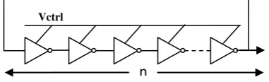
[image:4.595.301.554.94.774.2]The VCO is an ideal integrator with gain . A classical Voltage Controlled Oscillator based on a ring oscillator topology has been extensively used in the designer of Phase Locked Loops system; its operation is similar to a ring oscillator. The implementation of a ring oscillator, as Fig.11 shows [18]-[19], requires connecting odd number of inverters and feedback from the output of the last stage to the input of the first stage.
Fig.11. Classical voltage controlled ring oscillator The oscillation frequency of VCO is determined by the control current , number of stages N, the amplitude and parasitic capacitance [18], [19]. The frequency of the oscillation can be found as:
Where τ is the delay for one stage, which could be given by:
is the oscillation amplitude and is the control current. From the above equations (11) and (12), we can get (13).
The transfer gain of the VCO is found from the ratio of output frequency deviation to a corresponding change in control voltage. That is:
=
(14)
Where is the output frequency corresponding to , and is the output frequency corresponding to .
The oscillation frequency of VCO has been divided via a DBN before it’s fed back to the input of PFD. The implementation of divide by 8 counters, as presented in Fig.12, which is designed by cascading three divide by 2
circuit. It receives a clock signal of a predetermined frequency provided via VCO and generates a pulse for every 8 cycles of the clock signal.
Fig 12: Divide by 8 Counters
The open-loop transfer function of the CP-PLLs in Fig.5 is given by:
LG(s) =
(16)
The closed-loop transfer function of the CP-PPLs in Fig.5 is given by:
CG(s) = =
(17)
=
(18)
Conventional CP-PLLs has three poles and a zero. The third pole is introduced in order to attenuate the ripple which appears due to the nature of the CP-PLLs. As mentioned, the loop has a zero and three poles and the conceptual bode plot is shown in Fig.13.
Fig.13. Third-Order Loop Bode Plot Where is the zero and is the poles frequency
= (19)
= =0 (20) =
(21)
The phase margin degradation due to the third pole for CP-PLLs is obvious and is mathematically expressed by:
PM= arctan ( )+ arctan (
) (22)
4.
BEHAVIORAL SIMULATIONS
The results derived in the previous section are now verified in behavioral simulations. This section presents the behavioral modeling of Charge Pump-Phase Locked Loops in the context of a behavior design. Using simplorer, all blocks of CP-PLLs are modulated and designed by using hardware description
n
Vctrl
Phase Margin
Frequency
-180 -90
Frequency
40db/ decade
Amplitude (db)
20db/ decade
40db/ decade
[image:4.595.315.540.101.380.2] [image:4.595.59.250.447.505.2]language VHDL-AMS (Very High Hardware Description Language for Analog and Mixed Systems). Such behavioral models provide the advantage of short simulations time without compromising the fundamental functionality of CP-PLLs architecture. Basic VHDL-AMS model [20] has the same structure than VHDL. Both of them have two main parts: ENTITY and ARCHITECTURE, but there are some differences in each part. In these models, the behavior of this structure is inscribed directly in architecture by using concurrent, simultaneous or sequential statements.
Behavior model is described and modulated by expressing the evolution of the output signals according to those input signals independents of its internal structure; transistors level. In behavioral simulations, the CP-PLL is designed for a range frequency of 863 MHz to 870 MHz and a bandwidth of 63 KHz. The corresponding loop parameters are chosen using the design methodology described in section 3. For further information, literal expressions used to modulate the operation of different CP-PLLs blocks are illustrated in section3.
The equivalent electrical circuit of Charge Pump-Phase Locked Loops system synthesized from a hardware description language VHDL-AMS by using simplorer platform is shown in Fig.14.
Fig.14. Equivalent Electrical Circuit of CP-PLLs The transition cycle of the PFD for different states of its input signals, it’s respectively the reference signal and the feedback signal, also the functioning of CP for different states of PFD terminals is shown in Fig.15.
Fig.15. Response of PFD-CP combination
Firstly, if the rising edge of signal leads the rising edge then Up goes high ( =0) while Down remains low a time equal to the phase difference between and ; consequently is positive.
Secondly, when the rising edge of signal leads the rising edge then Up remains low ( ) while Down goes high a time equal to the phase difference between and
; consequently is negative.
Finally, if reference signal is in phase with feedback signal then Up ) and Down goes high a time
equal to a some ps. After this time Down and Up ) move at low levels; consequently is null.
The proper function of the loop filter is simulated using the equation described in section 3. Fig.16 showed its charging and discharging period operation mode. When is positive, the LF operated in the charge period and its output voltage rises. In opposite case, is negative, the LF operated in the
discharge period and its output voltage falls. Finally, in case where is null, the LF operated in the neutral period and its
output voltage maintains its previous states.
Fig.16. Charging and Discharging Period of the LF The control voltage (VCO input) and the VCO output (oscillation frequency: ) are simulated and the results are shown in Fig.17.
Fig.17. VCO Input/VCO Output
When the LF operated in charge period; the oscillation frequency of VCO increases, consequently having the effect of moving the edges closer together.
If the control voltage falls, LF operated in the discharge period, then the oscillation frequency of VCO decrease; consequently having the effect of moving the edges closer together.
In case where the LF operated in the neutral period, the oscillation frequency of VCO remains stable. When the output voltage of LF is null, the VCO oscillate at its central frequency .
The Divide by N block divides by N ( = /N), the results obtained by simulation are shown in Fig.18.
Fig.18. Output States of the Divide by 8 Counters Table.2 summarized the results obtained by behavioral simulations. It is illustrates respectively the transition cycle of CP-PFD. Also, the operation mode of LF, where is charge and discharge period. Finally, we illustrate the various values of the oscillation frequency of VCO and the output signals of DBN.
Sref.v al
Sfdb.val
PFD.up
PFD.dow n
Inv ers eus...
gate_tr ans ...
CP.ipump ...
10...
Table.2. Summary of Different Results
Leads
Leads
in phase
with
U 1 0 10
Down 0 1 10
0 1 01
Down 0 1 10
positive current
210µA
negative current -210µA
null current 0µA LF charge period
rises.
dicharge period
falls
maintains
previous states
VCO increase decrease =
DBN /N /N /N
Table.3 illustrates the characteristics of CP-PLLs design, where shows that has a good performance.
Table.3. Performances Parameters of CP-PPLs
Parameters This Works
Power Supply 2V
210µA
R1 12Ω
C1 9.5pF
C2 0.95pF
Range Frequency 863MHz to 870MHz
80 kHz
63KHz
7MHz/V
Ratio N divider 8
5.
CONCLUSION
The dynamics of CP-PLLs can be accurately analysis and described using state equations of Phase Freqyency Detectro. In this paper, a simple s-domain analysis of a third-order CP-PLLs has been presented in detail using the state equations of PFD. Based on this analysis, the CP-PLLs can be easily modeled and evaluated from specifications. The behavioral simulations results in simplorer using VHAL-AMS allow to verified the proposed analysis method and indicate the practical CP-PLLs system. The Different results were firstly allowed to verify the proper operation of developed behavioral models. Then, frequency analysis allows validating the proper functioning of this system. This generic analysis can be extended to other PLL systems.
ACKNOWLEDGMENTS
This work was supported by Laboratory of Electronic and Micro-technology Communication (EMC), National School of Engineering Sfax, University of Sfax, Tunisia.
REFERENCES
[1] I. Young, J. Greason, and K. Wong, ‘‘PLL clock generator with 5 to 10MHz of lock range for microprocessors’’, IEEE J. Solid-State Circuits, vol. 27, pp. 1599-1607, Nov. 1992.
[2] M. Meghelli, B. Parker, H. Ainspan, and M. Soyuer, ‘‘SiGe BiCMOS 3.3-V clock and data recovery circuits for 10-Gb/s serial transmission systems,’’ IEEE J. Solid-State Circuits, vol. 35, pp. 1992-1995, Dec. 2000.
[3] H. Rategh, H. Samavati, and T. Lee, ‘‘A CMOS frequency synthesizer with an injection-locked frequency divider for a 5-GHz wireless LNA receiver,’’ IEEE J. Solid-State Circuits, vol. 35, pp. 780-787, May. 2000.
[4] C. Munker, B.-U. Klepser, B. Neurauter, and C. Mayer, Digital RF CMOS transceivers for GPRS and EDGE, in IEEE Radio Frequency Integrated Circuits (RFIC) Symp. Dig. of Papers, 2005, pp. 265–268.
[5] J. Hein and J. Scott, ‘‘z-domain model for discrete-time PLLs,’’ IEEE Trans. Circuits Syst, vol. 35, pp. 1393-1400, Nov. 1998.
[6] F. M. Gardner, Charge-Pump Phase-Lock Loops, IEEE Trans. Communication, vol. COM-28, 1849–1858, Nov. 1980.
[7] I. Novof, J. Austin, R. Kelkar, D. Strayer, and S. W Syatt, ‘‘Fully inte-grated CMOS phase-locked loop with 15 to 240MHZ locking range and 50ps jitter,’’ IEEE J. Solid-State Circuits, Vol. 30, pp. 1259-1266; Nov. 1995.
[8] J. Maneatis, ‘‘Low-jitter process-independent DLL and PLL based on self-biased techniques,’’ IEEE J. Solid-State Circuits, Vol. 31, pp. 1723-1732; Nov. 1996.
[9] Pavan Kumar Hanumolu, Merrick Brownlee, Kartikeya Mayaram, and Un-Ku Moon, ‘‘Analysis of Charge Pump Phase Locked Loops’’, IEEE Transactions on circuits and systems, Vol. 51, No.9; September. 2004.
[10]Volodymyr Kratyuk, Pavan Kumar Hanumolu, Un-Ku Moon, and Kartikeya Mayaram,’’ Design Procedure for All-Digital Phase-Locked Loops Based on a Charge-Pump Phase-Locked-Loop Analogy;’’ IEEE Transactions on circuits and systems, II: Express Briefs, Vol. 54, No. 3, March. 2007.
[11]B Razavi, Monolithic, Phase-Locked Loops and Clock Recovery Circuits; Theory and Design, IEEE Press 1996.
[12]Intissar Toihria, Rim Ayadi and Mohamed Masmoudi, An Effective CMOS Charge Pump-Phase Frequency Detector Circuit for PLLs Applications, International Multi-Conference on Systems, Signals & Devices (SSD) Hammamet, Tunisia, March 18-21, 2013.
[13]Intissar Toihria, Rim Ayadi and Mohamed Masmoudi, Design of an Effective Charge Pump-Phase Locked Loops Architecture for RF Applications, International Journal of Computer Applications, Volume 74– No.3, July 2013.
[14]F.M. Gardner, Phase Lock Techniques, 2nd ed., New York, Wiley, 1979.
[15]Deng Wen-Juan, Liu Shubo, Wang Song, Chen Jian, Zou Jijun, On The Design Of The Charge Pump PLL In Video Decoder, Journal of Theoretical and Applied Information Technology, 15th October 2012. Vol. 44 No.1
[16]Debashis Mandal and T. K. Bhattacharyya, Implementation of CMOS Low-power Integer-N Frequency Synthesizer for SOC Design, Journal of Computers, VOL. 3, NO. 4, Avril 2008.
[17]K. Holladay, Design a PLL for specific loop bandwidth, END EUROPE, pp 64-66, October 2000.
[18]A Novel Built-In Self-Test Architecture for Charge-Pump Phase Locked Loops. J. Ramesh and K.Gunavathi. ICGST-PDCS Journal, Volume 7, Issue 1, May, 2007
[19]Retdian, N., Takagi, S. and Fujii, N., “Voltage controlled ring oscillator with wide tuning range and fast voltage swing”, IEEE Asia-Pacific Conference, ASIC on 2002. Proceedings, pp 201 – 204, Aug. 2002.