Design, Development and Implementation of ALU, RAM
and ROM for 8051 Microcontroller on FPGA using VHDL
Siddalingesh S. Navalgund
Assistant Professor
Dept. of Electronics and Communication Engg. SDM College of Engineering and Technology,
Dhavalagiri Dharwad
Prakash R Tonse
P.G. Student
Dept. of Electronics and Communication Engg. SDM College of Engineering and Technology,
Dhavalagiri Dharwad
ABSTRACT
Reconfigurable systems offer a solution to solve complex problems by combining the speed of hardware with the flexibility of software to improve performance and system performance. Past three decades have seen the introduction of the technology that has radically changed the way one analyses and controls the world around them. A byproduct of Microprocessor development by Intel is the 8051 Microcontroller which finds its use in almost all walks of life. The Microcontrollers are not as well known to the general public, or even the technical community, as are the more glamorous Microprocessors. The public is however very well aware that “something” is responsible for all the Smart VCRs, clock radios, washers and dryers, video games, TVs etc. That “something” is nothing but the Microcontroller.
Any Microcontroller consists of three main components viz., an Arithmetic and Logic Unit (ALU), a Random Access Memory (RAM) and a Read Only Memory (ROM). An ALU is responsible for Arithmetic and Logic operations like addition, subtraction, multiplication, AND, OR, NOT etc operations. RAM is meant for storing and retrieving the data whenever necessary and ROM serves the purpose of storing the definitions pertaining to the executions corresponding to the opcodes.
This paper presents the design, development and implementation of an Arithmetic and Logic Unit (ALU), a Random Access Memory (RAM) and a Read Only Memory(ROM) for 8051 Microcontroller on Field Programmable Gate Arrays (FPGA) using VHDL i.e., VHSIC Hardware Description Language where VHSIC stands for Very High Speed Integrated Circuits. Xilinx Spartan-3 xc3s50pq208-5 has been chosen as the target FPGA device. The device utilizations for ALU, RAM and ROM have been analyzed and tabulated to explore the design space
Keywords
ALU, RAM, ROM, Microcontroller, VHDL, FPGA.
1.
INTRODUCTION
[[[We Microcontroller manufacturers have been competing for a long time for attracting choosy customers and every couple of days a new chip with a higher operating frequency, more memory and upgraded A/D converters appeared on the market.
However, most of them had the same or at least very similar architecture known in the world of microcontrollers as “8051 compatible”. What is all this about? The whole story has its beginnings in the far 80s when Intel launched the first series
of microcontrollers called the MCS 051. Even though these microcontrollers had quite modest features in comparison to the new ones, they conquered the world very soon and became a standard for what nowadays is called the microcontroller.[1]
The main reason for their great success and popularity is a skillfully chosen configuration which satisfies different needs of a large number of users allowing at the same time constant expansions (refers to the new types of microcontrollers). Besides, the software has been developed in great extend in the meantime, and it simply was not profitable to change anything in the microcontroller’s basic core. This is the reason for having a great number of various microcontrollers which basically are solely upgraded versions of the 8051 family. [2]
2.
LITERATURE REVIEW
perform 16 operations which include both logical and arithmetic operations. Data retention and leakage current are among the major area of concern in today’s CMOS technology. In the paper [9] 6T SRAM cell has been analyzed on the basis of read noise margin (RNM), write noise margin (WNM), read delay, write delay, and data retention voltage (DRV). Implementation and simulations are carried out using VHDL. Paper [10] discusses the FPGA implementation about DDR3 SDRAM controller for high performance. Work by Vikas Gupta et. al. [11] explains a method for designing and implementing multiplierless digital PID controller based on Field Programmable Gate Array (FPGA) device. Paper [12] explains design of full architecture of an embedded processor for realizing arithmetic, logical, shifting and branching operations.
3.
THE 8051 MICROCONTROLLER
Like all good things, this powerful component i.e., Microcontroller is basically very simple. It is made by mixing tested and high- quality "ingredients" (components) as per following recipe:
1. The simplest computer processor is used as the "brain" of the future system.
2. Depending on the taste of the manufacturer, a bit of memory, a few A/D converters, timers, input/output lines etc. are added.
3. All that is placed in some of the standard packages.
4. Simple software able to control it all and which everyone can easily learn about has been developed.
On the basis of these rules, numerous types of microcontrollers were designed and they quickly became man's invisible companion. Their incredible simplicity and flexibility conquered mankind a long time ago and if one tries to invent something about them, one should know that they are probably late; someone before you, has either done it or at least has tried to do it [2].
3.1 Operation of Microcontroller
Even though there are a large number of different types of microcontrollers and even more programs created for their use only, all of them have many things in common. Thus, if you learn to handle one of them you will be able to handle them all. A typical scenario on the basis of which it all functions is as follows:
1. Power supply is turned on and everything starts to happen at high speed! The control logic unit keeps everything under control. It disables all other circuits except quartz crystal to operate. While the preparations are in progress, the first milliseconds go by.
2. Power supply voltage reaches its maximum and oscillator frequency becomes stabilized. SFRs are being filled with bits reflecting the state of all circuits within the microcontroller. All pins are configured as inputs. The overall electronics starts operation in rhythm with pulse sequence. From now on the time is measured in micro and nanoseconds.
3. Program Counter is set to zero. Instruction from that address is sent to instruction decoder which recognizes it, after which it is executed with immediate effect.
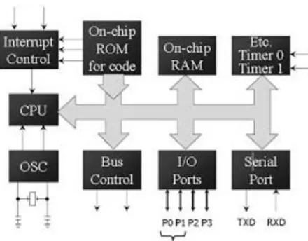
[image:2.595.320.540.69.241.2]4. The value of the Program Counter is incremented by 1 and the whole process is repeated several million times per second.
Figure 1: Basic view of Intel 8051 Architecture
As one can observe, all the operations within the microcontroller are performed at high speed and quite simply, but the microcontroller itself would not be so useful if there are not special circuits which make it complete.
The main components which aid in making any Microcontroller powerful are as follows.
Read Only Memory (ROM)
Read Only Memory (ROM) is a type of memory used to permanently save the program which is being executed.
Random Access Memory (RAM)
Random Access Memory (RAM) is a type of memory used for temporary storing data and intermediate results created and used during the operation of the microcontrollers.
Electrically Erasable Programmable ROM (EEPROM) The EEPROM is a special type of memory not contained in
all microcontrollers. Its contents may be changed during program execution (similar to RAM), but remains permanently saved even after the loss of power (similar to ROM).
Special Function Registers (SFR)
Special function registers are part of RAM memory. Their purpose is predefined by the manufacturer and cannot be changed. Since their bits are physically connected to particular circuits within the microcontroller, such as A/D converter, serial communication module etc., any change of their state directly affects the operation of the microcontroller or some of the circuits. For example, writing zero or one to the SFR controlling an input/output port causes the appropriate port pin to be configured as input or output. In other words, each bit of this register controls the function of one single pin.
Program Counter
Program Counter is an engine running the program and points to the memory address containing the next instruction to execute. After each instruction execution, the value of the counter is incremented by 1. For this reason, the program executes only one instruction at a time just as it is written.
Central Processor Unit (CPU)
1.Instruction decoder
2.Arithmetical Logical Unit (ALU) 3.Accumulator
Input/output ports (I/O Ports)
In order to make the microcontroller useful, it is necessary to connect it to peripheral devices. Each microcontroller has one or more registers (called a port) connected to the microcontroller pins.
Oscillator
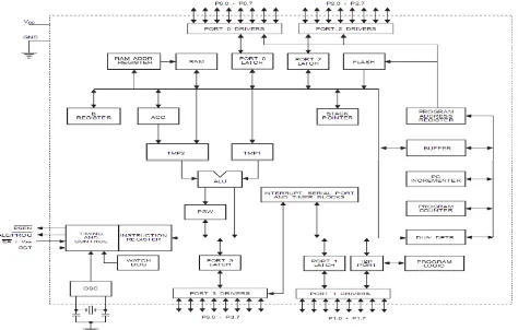
Even pulses generated by the oscillator enable harmonic and synchronous operation of all circuits within the microcontroller. It is usually configured as to use quartz-crystal or ceramics resonator for frequency stabilization. The AT89S51 is a low-power, high-performance CMOS 8-bit microcontroller with 4K bytes of in-system programmable
[image:3.595.70.544.235.537.2]Flash memory. The device is manufactured using Atmel’s high-density nonvolatile memory technology and is compatible with the industry-standard 80C51 instruction set and pin out. The on-chip Flash allows the program memory to be reprogrammed in-system or by a conventional nonvolatile memory programmer [1,2]. By combining a versatile 8-bit CPU with in-system programmable Flash on a monolithic chip, the Atmel AT89S51 is a powerful microcontroller which provides a highly-flexible and cost-effective solution to many embedded control applications. Detailed architecture of Atmel’s 8051 Microcontroller can be seen in figure 2 as described in Atmel’s data sheet.
Figure 2: Architecture of 8051 Microcontroller [11]
4.
DESIGN AND IMPLEMENTATION
The programming environment for ALU, RAM and ROM is based on VHDL. The behavioral description of the functionality is initially written and is then analyzed, simulated and synthesized onto Xilinx FPGAs. An application for the ALU, RAM and ROM modules implementation is developed by writing behavioral description in VHDL and the description is iteratively refined and debugged with the simulator available i.e., ModelSim version 5.5 a. After the description code is verified to be functionally correct by simulation, it is translated onto a Xilinx net list form. The net list is then mapped onto FPGA architecture by automatic partition, placement and routing tool to form a loadable FPGA object module. A static timing analysis tool is then applied to the object module to determine maximum operating speed.
4.1 Entity Declaration
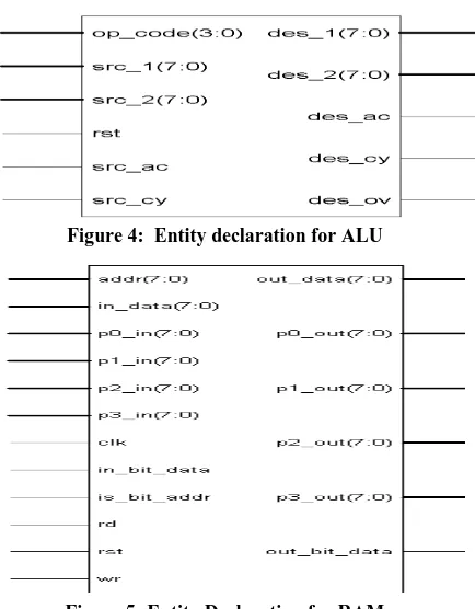
Entity declaration implies declaring input and output ports for the required design. The ALU receives op_code, a 4-bit input and two inputs of 8 bits each i.e., src_1 and src_2. The ALU is provided with reset signal rst. It is also provided with an auxiliary carry (src_ac) and carry (src_in) as two more inputs to aid arithmetic operations. It has two 8-bit outputs i.e., des_1 and des_2 and three single bit outputs auxiliary carry out (des_au), carry out (des_cy) and overflow bit(des_ov) . The entity declaration for an 8-bit ALU can be seen in Figure 4.
[image:3.595.325.537.680.747.2]Figure 4: Entity declaration for ALU
Figure 5: Entity Declaration for RAM
Following the same methodology entity for RAM can be declared. It has an active high reset pin (rst), when asserted, the registers are set to default values, a clk (rising edge) : clock signal - all ram i/o is synchronous, an 8-bit address bus (addr), in_data pin which specifies the data being written into the ram/reg, an 8-bit out_data pin to read data from the ram/reg, a in_bit_data pin to write into the ram/reg, an out_bit_data pin for reading bit data from the ram/reg, an active low read signal (rd) which is asserted to signal a ram/reg read, an active low write signal (wr) asserted to signal a ram/reg write, an active high is_bit_addr pin for asserting if requesting a ram/reg bit-data and four 8-bit input and output ports. Entity declaration for ROM can be seen in Figure 3 and
entity declaration for ALU can be seen in Figure 4. The ROM has a 16-bit address bus (addr), a clock pin (clk), a read pin (rd), a reset pin (rst) and an 8-bit data bus. This read only memory serves the purpose of permanently storing the required functionality.
5.
RESULTS AND DISCUSSIONS
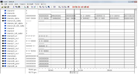
[image:4.595.321.540.293.439.2]Our The behavioral description of the ALU, RAM and ROM is behaviorally described and synthesized using Xilinx ISE version 7.1i and simulated and functionally verified on the ModelSim version SE 5.5a simulator. The simulation results of ALU performing Multiplication Operation can be seen in Figure 7. Here depending on the value of op_code the various arithmetic and logic operations get executed. The simulation results are up to the expectations and hence the functionality of the code is verified. Further test bench is written in order to check the veracity of the HDL code. The .mcs file being generated is dumped on to FPGA (Spartan) which can be seen in the figure 6. The output snapshot depicts simple addition operation with overflow being detected.
[image:4.595.73.545.504.698.2]Figure 6: Output snapshot of ALU on FPGA
Figure 8: RTL schematic for Read Only Memory
Figure 9: Simulation result for Arithmetic and Logic Unit(ALU)
[image:5.595.73.550.494.750.2]Figure 11: Simulation results for Read Only Memory (ROM)
In the similar fashion the behavioral description for RAM is described using VHDL and the simulation results can be seen in Figure 10. The behavioral simulation for ROM can be seen in Figure 11. The RTL schematic for the designed ALU can be seen in Figure 7 and for the ROM in figure 8. The Register Transfer Level logic is up to the expectations as that of the
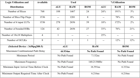
8051 architecture. As the entire code for all the three modules is synthesizable, the synthesis is carried out on the FPGA device (Spartan 3s50pq208-5). The entire design is optimized for speed and area using Xilinx device family Spartan. The device utilization, timing report, logic distribution and other details are given in Table 1.
TABLE 1: DEVICE UTILIZATION SUMMARY FOR ALU, RAM AND ROM USING XILINX XST
Logic Utilization and
Distribution
Available Used %Utilization
ALU RAM ROM ALU RAM ROM
Number of Slices 768 188 1467 24 24% 191% 3%
Number of Slice Flip Flops 1536 -- 1201 8 -- 78% 0%
Number of 4 input LUTs 1536 278 2656 39 18% 172% 2%
Number of bonded IOBs 124 42 2656 27 33% 76% 21%
Number of 18x18 Multipliers 4 1 -- -- 25% -- --
Number of GCLKs 8 -- 1 1 -- 12% 12%
(Selected Device : 3s50pq208-5)
Maximum Combinational Path Delay
ALU RAM ROM
44.934ns No Path Found No Path Found
Minimum Period No Path Found 7.132ns No Path Found
Maximum Frequency No Path Found 140.213MHz No Path Found
Minimum Input Arrival Time Before Clock No Path Found 16.591ns 6.333ns
Minimum Output Required Time After Clock No Path Found 6.216ns 6.216ns
6.
CONCLUSION
In this paper an attempt has been made to implement Arithmetic and Logic Unit (ALU), a Random Access Memory (RAM) and a Read Only Memory (ROM) specific for 8051 Microcontroller on Field Programmable Gate Array (FPGA) using VHDL as the hardware description language.
[image:6.595.53.542.394.668.2]7.
ACKNOWLEGEMENT
The authors thank the authorities of Sri Dharmasthala Manjunatheshwara College of Engineering and Technology, Dhavalagiri, Dharwad, Karnataka, India for encouraging us to carry out this research work. The first author specially thanks TEQIP 1.2 for providing the teaching/research assistantship for the period of March-2013 to July-2013.
8.
REFERENCES
[1] Kenneth J Ayala, West Carolina University, “The 8051 Microcontroller, Architecture, Programming and Applications”, West Publishing Company, St Paul. ISBN 0-314-77278-2.
[2] Online tutorial by MikroElektronika on “Architecture
and programming of 8051 MCU's”
http://www.mikroe.com/ chapters/view/64/chapter-1-introduction-to-microcontrollers.
[3] Shrivastava Purnima, Tiwari Mukesh, Singh Jaikaran and Rathore Sanjay, “VHDL Environment for Floating point Arithmetic Logic Unit - ALU Design and Simulation”, Research Journal of Engineering Sciences Vol. 1(2), 1-6, August (2012), ISSN 2278 – 9472,pp: 1-6
[4] Shikha Khurana and Kanika Kaur “Implementation Of ALU Using FPGA” ,International Journal of Emerging Trends & Technology in Computer Science (IJETTCS), Volume 1, Issue 2, July – August 2012 ISSN 2278-6856, pp:146-149avel, P. 2007 Modeling and Simulation Design. AK Peters Ltd.
[5] Vandana Parihar and Dr. R.C.Jain, “Performance based Configuration and Implementation of Hash Processor” International Journal of Advance Technology & Engineering Research (IJATER) , Vol. 1, Issue 1, November 2011, ISSN NO: 2250-3536. Pp: 54-58.
[6] Ashwini S. Deshmukh, “A Novel FPGA based Leading One Anticipation Algorithm for Floating Point Arithmetic Units” International Journal of Reconfigurable and Embedded Systems (IJRES) Vol. 1, No. 1, March 2012, ISSN: 2089-4864 , pp. 19-24.Brown, L. D., Hua, H., and Gao, C. 2003. A widget framework for augmented interaction in SCAPE.
[7] Suma T.Hegde, Dr. Siva Yellampalli and Nandeesh R, “Design and Implementation of ALU using Redundant Binary Signed Digit”, International Conference on VLSI, Communication & Instrumentation (ICVCI) 2011, Proceedings published by International Journal of Computer Applications® (IJCA), pp: 30-35.
[8] Geetanjali and Nishant Tripathi, “VHDL Implementation of 32-Bit Arithmetic Logic Unit (ALU ” International Journal of Computer Science and Communication Engineering, IJCSCE Special issue on “Emerging Trends in Engineering” ICETIE 2012. Pp: 41-44
[9] Mahendra Kumar and Kailash Chandra “Low Power High Performance SRAM Design Using VHDL”, Global Journal of Researches in Engineering, Volume 11 Issue 1 Version 1.0 February, 2011, ISSN: 0975-5861, pp: 21-24
[10] Shabana Aqueel and Kavita Khare, “Design and FPGA Implementation of DDR3 SDRAM Controller for High Performance” , International Journal of Computer [11]Prof. Vikas Gupta, Dr Kavita Khare and Dr R. P. Singh
“Efficient FPGA Design and Implementation of Digital PID Controllers in Simulink®”, International Journal of Recent Trends in Engineering, Vol 2, No. 6, November 2009, pp:147-150
[12]Mr. Sumedh. S. Jadhav, and Prof. C. N .Bhoyar, “Implementation of Embedded Multiprocessor Architecture Using FPGA”. International Journal of Scientific & Engineering Research, Volume 3, Issue 1, January-2012, ISSN 2229-5518, pp 1-6.
[13]Data Sheet of Atmel’s AT89S52 Microcontroller. www.atmel.com/images/doc1919.pdf
AUTHOR’S PROFILE
Siddalingesh S. Navalgund received Bachelor of Engineering in Electronics and Communication Engineering from Karnataka University Dharwad in 2000 and Master of Technology in Microelectronics and Control Systems from Visvesvaraya Technological University, Belgaum in 2004. After spending two years in the industry, he joined as a faculty in N. M. A. M. in Institute of Technology, Nitte, and Karnataka. Since 2005, he is serving as faculty in the Dept. of E&CE, S. D. M. College of Engineering and Technology, Dharwad, Karnataka. His main research interests include VLSI design, embedded & fuzzy systems and digital signal processing.
Mr. Navalgund is currently the life member of Institution of Electronics and Telecommunication Engineers (IETE), Indian Society for Technical education (ISTE) and Institution of Engineers India (IE-I).