Design of a Novel Reversible Arithmetic Circuit using
QCA
Ritika Jain
Lovely Professional University,India
ABSTRACT
Reversible logic is one of the flourishing importance to many futuristic technologies. A reversible circuit maps each input vector into a unique output vector. There should not be any information loss in the circuit, because it is proved that each irreversible bit operation dissipate kTln2 amount of energy, but there are so many fields such as cryptography, optical computing, DNA computing etc., where such kind of information loss augments the heat dissipation. As the circuits are getting more compact, soon a limitation to Moore’s Law will be reached hence further no more transistors can be mounted on a single chip. Therefore the next era of technology is transistor less circuit, in which the same operations which are performed now using transistors will be processed at atomic or molecular level using transistor less technique i.e. Quantum Dot Cellular Automata. A novel Reversible Gate RSG is proposed which is designed using QCA. RSG gate outperforms existing reversible gates in terms of garbage outputs and multi functionality.
General Terms
Reversible Computing, Quantum Computing, QCADesigner 2.0.3
Keywords
RSG, QCA, Quantum Cost, Garbage Output, Multifunctional, HA, HS.
1.
INTRODUCTION
Reversibility is a term defined as retaining the initial state of any system through its final state. Precisely it can be said as a system with no information loss. This can be simply understood by day to day examples, consider chemical reactions. These reactions can be reversible or irreversible. In irreversible reactions reactants can not be retained through its products, means once formed product cannot be converted back to its raw materials. But in reversible equations reactants can be preserved through products, means nothing is lost. Reversible circuits also work on the same principle; more precisely if we are able to attain inputs back to each output combination then the circuit or system becomes reversible. This approach is generally unusual. Reversibility in circuits is a forecasting computing methodology in Quantum Computing, Optical Computing, Nano-technology, DNA Technology and cryptography etc. Reversible computing can only be achieved through reversible gates. In these circuits unique output combination is generated for each unique input pattern, consequently no information is lost and when there is no information loss then according to Bennet circuit exhibits zero power degeneracy [3]. As it is proposed by Landauer that per irreversible bit operation contributes in kT ln2 amount of heat dissipation [2], but if circuits are made reversible then this loss can be oppressed.
Conditions for a gate to be reversible are as follows: Same input and output counts
Any kind of loop or feedback is not permissible One to One mapping
No Fan Out is allowed .
2. REVERSIBLE LOGIC
The concept of reversibility elevated in 1970s. There were two tempting concerns for physical reversibility and logical reversibility. A logic will be said physically reversible when no heat dissipation occurs during operation, because in this case there will be no irreversible bit operation, hence there will be no change in entropy. Other way around if we can reconstruct the inputs through outputs uniquely then the system will be termed as logically reversible. The logic for reversible computation is shown in Fig. 1. Here a n x n logic is described with A1, A2…An as inputs and Y1, Y2…Yn as
outputs.
A1 Y1
A2 Y2
An Yn
Fig 1:Reversible Logic
The concept of both type of reversibility can be understood with a simple illustration of fundamental OR gate. As OR gate has two inputs and one output, hence it is very much clear that one of its input is completely washed off because we have single output, this removal of one input will turned into information loss to the system. This information loss will contribute in irreversible bit operation resulting in kT ln2 amount of heat dissipation, therefore OR gate is not physically reversible. According to the functionality of OR gate, output results high voltage or logic 1 in three cases, but by looking at the output one cannot predict the input combination for which circuit is giving logic 1, therefore OR gate is not logically reversible.
2.1 Reversible Gates
As reversibility condition are mandatory for a gate to behave as reversible. All quantum circuits are by necessity reversible. It is also postulated that quantum circuits used in quantum computers are required to be reversible up to some extent. Reversible gate is a basic cell of reversible circuit, which can be further extended to build large reversible circuits. In the literature till now many authors have proposed many
reversible gates, though some of them are universal and widely used. To transform any irreversible logic function into reversible logic, few terms are needed to be looked before proceeding further.
Garbage Output: The extra pins in the outputs are added to make a function reversible; these extra outputs are called garbage output. These are inserted just to maintain the reversibility of the logic. These pins are always added in outputs. Garbage outputs by explanation are considered to be don’t cares [4]. Ancilla Bit: The constant pins added in inputs to
make equal input and output counts are called ancilla bits. These can take values of either 0 or 1. These bits play important role when we need to design cascaded circuits for the propagation of information.
There are two more terms regarding reversible gates, these are explained below.
Multi-functionality: Reversible gates can perform multiple operations by making one or more inputs constant either binary-1 or binary-0.
Quantum Cost: Each reversible gate or circuit can be used in quantum computing only when these gates are transformed into their equivalent quantum gate representation. The number of quantum gates used for designing circuit is equivalent to the circuit’s quantum cost and quantum delay.
2.2 Elementary Quantum Gates
Elementary quantum gates are the key elements for quantum computation. Qubit is the basic cell of a quantum computation.
Inverter (NOT): This operates like a conventional NOT gate, inverts the input qubit shown in Fig. 2.
A P=A
Fig 2: NOT Gate
[image:2.595.313.541.70.361.2] Controlled inverter (CNOT): In this aimed qubit is inverted if the source qubit is 1, this can be treated as xor operation. The symbol is shown in Fig.3.
A P=A
B Q= A B Fig 3: CNOT Gate
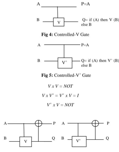
Controlled -V and V+ Gates: The V operation is square root of NOT gate shown in Fig.4.Controlled-V+ gate is inverse of square root of NOT gate shown in Fig.5.When controlled-V gate and Controlled-V+ gates are in successive order then, it results in identity matrix. When controlled-V gates are connected in series, acts as NOT Gate.A P=A
B Q= if (A) then V (B) else B
Fig 4: Controlled-V Gate A P=A
B Q= if (A) then V+ (B)
else B
Fig 5: Controlled-V+ Gate V x V = NOT
V x V+ = V+ x V = I V+ x V = NOT
A P A P
B Q B Q
Fig 6: Unit Quantum Cost Arrangements
All elementary gates are assumed to have unit cost [1]. Moreover, Fig.6 shows when a V or V+ gate is connected to CNOT between two same qubits, the cost of the pair can be considered as a unit [11].
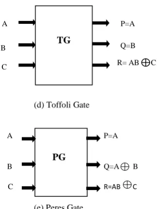
Some of existing reversible gates like Feynman Gate [10], Toffoli Gate [5], Peres Gate [15], Fredkin Gate, New Gate and NFT Gate [18] are shown in below Fig. 7.
A P=A B B Q= AC’ B’C
C R= AC’
BC
(a) NFT Gate
A P= A
B Q= A’B AC
C R=A’C AB
(b) Fredkin Gate
A P=A
B Q= A B
(c) Feynman Gate V
NFT
FRG
V+ V
V+
[image:2.595.375.526.463.740.2]R= AB C
(d) Toffoli Gate
A P=A
B Q=A B
C R=AB C
(e) Peres Gate
Fig 7: Reversible Gates
3. QUANTUM DOT CELLULAR
AUTOMATA
In contrast to electronics based on transistors, QCA does not work on the transport of electrons, but by the arrangement of electrons in a small limited area of only a few square nanometers. It is implemented by quadratic cells, therefore it is called QCA. Structure of basic QCA cell is shown in Fig. 8, in this small square, precisely four potential wells are located; one well is situated in each corner of QCA cell. The cell substrate can be constructed using semiconductors according to application. Electron Tunnel Junction is responsible for switching of electron from one potential well to another. In individual QCA cell exactly two electrons are sealed. These two electrons can only reside in the potential well.
Potential Well
Electron Tunnel Junction Cell Substrate
Fig 8: Structure of QCA Cell
Fig. 9 shows a general arrangement of electrons in single QCA cell.
Empty Potential
Well Electron in Potential Well
Fig 9:Electron Arrangement in Potential Well
There are two diagonals in a square, which means the electrons can dwell in exactly two possible variations in the QCA cell. Each cell can be in two states. Fig. 10 (a) shows a
null polarized QCA cell which corresponds to no fixed polarization, according to input signal it will change its polarization. More precisely polarization +1 is often interpreted as binary '1' and polarization -1 as binary '0' shown in Fig. 10 (b) and 10 (c) respectively.
(a) Null Polarized (b) Binary 1 (c) Binary 0 Fig 10: Polarization in QCA Cell
3.1 Information Flow in QCA Cell
If two QCA cells are placed near to each other then it is possible to interchange their states, The QCA cell that has to transfer its state to a neighboring cell must have its tunnel junctions locked, and the tunnel junctions in the neighboring cell have to be exposed, to allow the electrons to travel through the tunnel junctions between the potential wells. As soon as they expose, the electrons in the neighboring cell are pushed by the Coulomb force of the previous cell as far away as possible. As they also are pushed away from each other, they will go into the same potential wells as in the previous cell. As soon as the tunnel junctions are locked again, the transfer of the state is terminated [6].Binary information flows through QCA wire which can be designed in two ways such as 45• QCA wire and 90•QCA wire are shown in Fig. 11(a) and 11(b).
(a) 90• QCA Wire
[image:3.595.91.253.78.293.2](b) 45• QCA Wire Fig 11: QCA Wires
In 45• wire, the information propagation is altered at each cell, means the each successive cell inverts the incoming signal. Therefore if we want to propagate the original signal through 45• QCA wire, then we need to place odd number of QCA cells. This wire is useful when we need to make cross wire connections. But in 90• wire the same information is flown through out the wire.
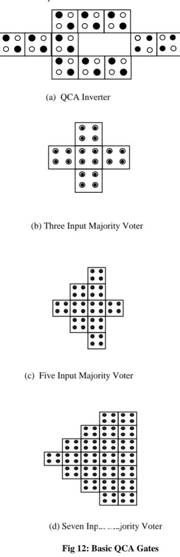
3.2 Elementary QCA Gates
The elementary gates are QCA inverter, three-input majority voter, five input majority voter and seven input majority voter. Following Fig. 12 shows all the basic QCA elementary gates. An inverter can be designed in QCA like shown in Fig.12 (a), this arrangement of cells result in highest polarization. Suppose ‘-1’ polarization is applied to the input, then before reaching to the second last cell, due to electrostatic repulsion the position of electrons get changed, therefore we get inverted signal at the output.
Three input majority voter shown in Fig. 12(b), it takes three inputs A, B & C, and depending on the majority input voters
PG
A
B C
P=A
Q=B
[image:3.595.317.526.143.206.2] [image:3.595.313.548.414.543.2] [image:3.595.53.266.648.701.2]the, output will take that value. Suppose, signal A and B have ‘+1’ polarization but C has ‘-1’ polarization, so according to majority voter condition ‘+1’ will be transferred to the output Y.
Similar working can be understood for five input majority voter and seven input majority voter shown in Fig. 12 (c) and Fig. 12 (d) respectively. The only difference is of number of inputs in majority voter, like five input majority voter [14] consists of five inputs and seven input majority voter [13] takes seven inputs.
(a) QCA Inverter
(b) Three Input Majority Voter
(c) Five Input Majority Voter
[image:4.595.57.236.174.726.2](d) Seven Input Majority Voter
Fig 12: Basic QCA Gates
By using these majority gates one can deduce any logic function like AND, OR, XOR etc. just by polarizing any cell to a fixed value.
3.3 Clocking Scheme
As Quantum -Dot Cellular Automata implementation does not require any power signal for its operation, all it needs is just proper clocking scheme. There are four different clocking zones, named as clock 0, clock 1, clock 2, clock 3 having different colors. The proper arrangement of these clocking is only responsible for exact results. Each clock signal is phase shifted by 90•. Four clock signals are adequate to control the propagation of information in a QCA circuit [8] [9].
These clocks synchronize as well as control the information propagation. These are the sources of power in QCA circuits. By using four phase clocking arrangement; QCA manages and propagates the information within the cells in a prescribed timing format. QCA cells are organized in a group having particular clock zone so that all the cells have same affecting field. Each clock zone has four phases named as switch, hold, release and relax. These four phases play a significant role in information propagation.
Switch: In this phase the electrons are affected by neighboring columbic charges as in this tunneling barrier is increased.
Hold: In this the state achieved by electrons are not changed and tunneling hindrance is very high. Release: In this phase tunneling hindrance is started
to slow down and cells are tied to their hold states. Relax: In this phase tunneling barrier is null and
cells are free to acquire new values.
The following Fig 13 shows the clocking scheme and Fig 14 shows four different phases of each QCA clock. It is mandatory to have proper clocking scheme, otherwise accurate results can not be achieved. These clocking scheme is responsible for design of QCA, this makes QCA distinctive from CMOS circuits [12] [15-17].
Fig 13: Clocking Scheme in QCA
The four phase of a clock in shown below in Fig 14, this is very significant feature of QCA clocking, according to this we need to place QCA cells so that proper flow of information is possible. In QCA when circuit becomes more complex, delay of the circuit may enhance because of more QCA cells and wire connections. Therefore it is very much important to group cells for each clock cycle for better propagation of information.
0
1
OUT
C
B
A
A
E D
C B
OUT
G F
E D
C B
A OUT
Clock Zone 0
Clock Zone 1
Clock Zone 2
[image:4.595.347.503.494.589.2]
Fig 14: Phase Description of a QCA Clock
[image:5.595.48.283.75.173.2]The Fig 14 shows a general four phase in a clock. Following Fig 15 shows the four phases and switching in different clock zones.
Time Switch Hold Release Relax Relax Switch Hold Release
Release Relax Switch Hold Hold Release Relax Switch
Fig 15: Phase in Clock Zones
4. PROPOSED DESIGN
[image:5.595.63.288.241.344.2]In designing section each time focus is on reduction in garbage outputs, input-output counts, quantum cost and moreover increasing multi-functionality. All the existing reversible gates work on a single operation like either these can be used as a reversible adder or reversible subtractor. But there is no such circuit which can be used as both adder and subtractor concurrently. Here a novel reversible RSG Gate is proposed which can perform both the operations simultaneously. This novel circuit does not use any control pin for selecting addition or subtraction operation. The block diagram of this novel gate is presented below in Fig 16. It is a 3x3 gate having A, B & C as inputs and P, Q & R as outputs.
Fig 16:Block Diagram of Proposed RSG
Table 1 shows the truth table of RSG gate. It shows correct results, according to equations of circuit. There are total eight input patterns and each pattern results in different and unique output pattern. Consider an input pattern 110, output P will perform XOR and will give value as 0, Q will give 1 and R will result in 0, hence output pattern will be 010.
Table 1. Truth Table of RSG
Table 2. Multifunctional RSG
[image:5.595.341.516.420.495.2]Table 2 shows the multi-functionality of proposed RSG gate. This gate can perform as reversible half adder and reversible half subtractor simultaneously.
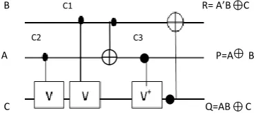
Fig 17:Quantum Gate Implementation of RSG
The proposed RSG gate is also designed using elementary quantum gates shown in Fig 17. For reducing the quantum cost, order of inputs and outputs are changed, but this will not affect the functionality of circuit. Though this way, quantum cost of circuit is reduced to five from seven.
Consider a case when input pattern is 110. Now A=1, B=1 and C= 0 thus control signals C1, C2 and C3 will have values 1, 1 and 0 respectively.
B C1 R= A’B C
C Q=AB C
Fig 18:Controlled signals C1, C2 and C3
Because C3 will result in xor operation as both high signals give 0. As C1 and C2 both are high and both V gates are in series means they will behave as NOT gate hence 1 will be the Switch Hold Release Relax
Clock 0 Clock 1 Clock 2 Clock 3
B
A
C
R
P
Q
C2 C3
A P=A B
A
B
C
RSG
P=A B
Q = AB C
[image:5.595.59.263.540.632.2] [image:5.595.349.535.616.701.2]output of this series connection. As C3 is 0 means same signal will pass to Q without any inversion and C3 pin value will be passed to P and R will have the value as 0 because 1 xor 1 will give 0.
RSG gate is designed and simulated using QCADesigner 2.0.3 tool [7] with 11 three input majority voter and 6 inverters shown below in the Fig 19. The starting of output is shown in blue boxes for every output.
(a) Layout of RSG using QCA
[image:6.595.340.516.78.188.2](b) Output
Fig 19:Implementation of RSG
5. RESULT & ANALYSIS
A comparative analysis of novel proposed gate is presented with existing gates in literature on the ground of garbage output, quantum cost, and multi-functionality.
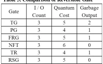
Table 3. Comparison of Reversible Gate
Table 3 shows the comparison of proposed RSG gate with existing gates present in the literature. RSG gate outperforms to existing gates in terms of garbage output. Since its quantum cost is five, but garbage count is zero. Though NFT gate also has garbage output as zero but its quantum cost is six.
Table 4. Comparison in Terms of Multi-functionality
[image:6.595.78.263.176.479.2]Table 4 shows a comparison among reversible gates on the ground of number of operations a gate can perform or in terms of multi-functionality. The results show that proposed RSG gate performs maximum of eight operations which makes it remarkable than other gates. Here HA refers to half adder and HS refers to Half subtractor. This is the only gate which performs both the operations simultaneously.
Fig. 20 shows the outperformer RSG gate. It depicts that RSG has maximum number of multi functional operation count of eight and garbage output as zero. For a good design we need to suppress garbage output to minimum and enhance operation count to maximum, proposed RSG gate is fulfilling both the criterion. Proposed gate has quantum cost and delay as 5 with maintaining I/O count as 3.
[image:6.595.315.544.279.412.2] [image:6.595.321.542.584.716.2]6. CONCLUSION
The proposed design RSG gate can be a basic cell for many DSP circuits and ALU where both the operations are needed simultaneously. This can be a core block in arithmetic logical unit; because a single gate can perform both the addition and subtraction operations simultaneously hence the selection pins can be used for another operation in ALU. This proposed gate can be further used in designing reversible multipliers, carry look ahead adders and ripple carry adders etc. The other way round, in this design a control pin is removed which further removes extra pin from the circuit. RSG gate has maximum number of operation count; therefore it can replace existing reversible gates in terms of multi-functionality.
7. REFERENCES
[1] A. Barenco and C. H. Bennett, et.al. , ” Elementary gates for quantum computation. Phys. Rev. A, 1995.
[2] R. Landauer, ”Irreversibility and heat generation in the computational process”, IBM J.Research and Development, 1961.
[3] C. H. Bennett , “Logical Reversibility of Computation,” IBM Journal of Research and Development, 1973. [4] D.Grobe et.al. ,”Exact Synthesis of Elementary Quantum
Gate Circuits for Reversible Functions with Don’t Cares”, 38th international Symposium on Multiple valued
Logic, 2008.
[5] T.Toffoli,”Reversible Computing,”MITLab for Computer Science, Tech.Rep.Tech memo MIT/LCS/TM-151, 1980.
[6] “Nano -Arch Online Quantum Dot Cellular Automata QCA”, University of Erlangen- Nurnberg 2012.
[7] W.Konard et.al. , ”QCADesigner: A Rapid Design and Simulation Tool For Quantum-Dot Cellular Automata”, IEEE Transactions on Nanotechnology, 2004.
[8] G. Toth and C. S. Lent, “Quasi adiabatic switching for metal-island quantum-dot cellular automata”, J. Appl. Physics, 1999.
[9] K. Hennessy and C. S. Lent, “Clocking of molecular quantum-dot cellular automata”, J. Vac. Sci. Technology B, 2001.
[10] Thapliyal H. and Ranganathan N., ”A New Design of The Reversible Subtractor Circuit”,11th
IEEE International Conference on Nanotechnology,2011. [11] Akeela R. and Wagh D., ”A five Input majority Gate in
Quantum-dot Cellular Automata”, 54th IEEE International Midwest Symposium on Circuit and Systems, 2011.
[12] Karthigai L. et.al., ”Design of Subtractor using Nanotechnology Based QCA”, IEEE International Conference on Communication Control and Computing technologies”,2010.
[13] Navi K. et.al., ”A Novel Seven Input Majority Gate In Quantum-Dot Cellular Automata”, IJCSI, 2012. [14] Navi K. et.al., ”Five-Input Majority Gate, a new Device
for Quantum-Dot Cellular Automata”, Journal of Computational and theoretical Nano science, 2010. [15] R. Zhang et. al., “A Method of Majority Logic Reduction
for Quantum Cellular Automata”, IEEE Transaction on Nanotechnology, 2004.
[16] Heumpil Cho et. al., “Adder Design and Analysis for Quantum Dot Cellular Automata”, IEEE Transaction on Nanotechnology, 2007.
[17] G.H.Bernstein et.al. , “Magnetic QCA System”, Micro Electronics Journal, Elsevier, 2005.