Minimizing Skew and Delay with Buffer Resizing and
Relocation during Clock Tree Synthesis
Preeti Punia, Rouble, Neeraj Kr. Shukla, and Mandeep Singh
Department of Electrical, Electronics & Communication Engineering
ITM University, Gurgaon (Haryana) India
ABSTRACT
Rapidly increasing design complexity due to small size and higher speed, results in the problem of clock skew and insertion delay. These are the two important parameters which should be considered for successful completion of the design. In this work, a method for minimizing clock skew by buffer insertion and resize is proposed. Clock skew will be minimized during post-CTS timing analysis after placement of standard cells during physical implementation of the design. Also, buffer relocation method is used for minimizing the delay of the cells. Simulations were carried out on EDA tools and results show that overall skew is improved by 23.95% and delay is improved by 19.50%.
Keywords
Buffer, CTS, Delay, Skew, Slack.
1.
INTRODUCTION
The premium challenge in the field of VLSI design nowadays is the designing of a VLSI chip using lower process technologies. As the design complexity is rapidly increasing due to the small design size, higher clock frequency and lower voltage, higher speed, the market windows continues to shrink. As a result, insertion delay and Clock skew are the two emerging dominant factors which should be managed in order to successfully complete designs in a precise manner. Now, simply by making improvements to existing tools and methodologies will not address the full extent of these issues. There are many design variable interdependencies which are to be dealt with. The most important amongst them is the trade-off between power consumption, routability, and timing. Optimization of one design variable can cause problems with the others. Large amounts of routing resources are consumed by power and clock networks. Their construction and analysis must be started early and they should be customized for an individual chip’s demand. Clock trees are inserted after the placement of standard cells is complete. Physical design is as important as logic design in determining whether the demands are achievable or not. Design size has surpassed the limitations of gate-level design tools. The chip must be planned at high level, partitioned into smaller pieces, and then design should be completed using lower level tools. During physical implementation of the design, we come across Clock Tree Synthesis (CTS). It is the process of buffer/inverter insertion along the clock paths of the design so as to achieve minimum skew or optimized skew. The premium goal of Clock Tree Synthesis is to minimize insertion delay and skew. The concept of useful skew can also be added in the design using inverters and buffers. The key factor in physical design is to optimize the slack values and the arrival times of the clock i.e., skew and delay to meet the timing requirement of the design.
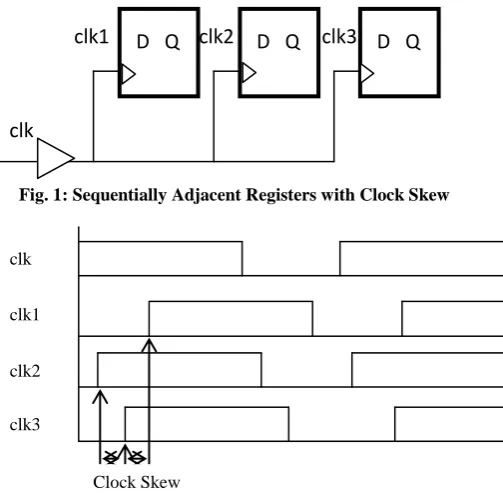
The slack can be defined as the difference between the required time and the arrival time of the clock pulse. A positive slack at a node implies that the arrival time at that node may be increased by a factor without affecting the overall delay of the circuit. Negative slack implies that a path is too slow, and the path must be speed up (or the reference signal delayed) if the whole circuit is to work at the desired speed. Clock skew is the difference between the actual and expected arrival time of a clock signal at two different flops. Clock skew results in slow system performance as it uses comparatively large time period between clock pulses. It can also cause set-up time or hold time violations. Therefore, clock skew must be minimized during clock routing. It is an elementary design principle that the timing should satisfy register’s setup and hold-time requirement. Timing violations may occur due to clocking of sequentially adjoining registers on the edge of a high skew clock i.e. the same clock edge and it can also be responsible for functional failures. Figure 3.1 represents sequentially-adjoining registers, in which a local routing structure is used for routing of the clock signal. Here, clock skew can be noticed. In Figure 1, all the three registers are clocked at the same clock edge. Here, each of the three registers has different arrival time of the clock edge. Figure 2 illustrates a case of the clock skew for the circuit shown in Figure 1.
clk1 clk2
clk3
[image:1.595.311.563.472.719.2]clk
Fig. 1: Sequentially Adjacent Registers with Clock Skew
Figure 2: Clock Arrival Time Fluctuations in the circuit of Figure 1
D Q
D Q
D Q
clk
clk1
clk2
clk3
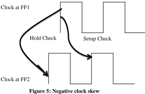
Mainly skew is of two types, positive skew and negative skew. Figure 3, 4 and 5 shows the case of zero, positive and negative clock skew.
Figure 3: Zero Clock Skew
[image:2.595.55.297.346.482.2]If the clock comes late than the launch time clock then it is called positive skew. In this case, data and clock flows in same direction. In other words, positive skew is when routing of the data and the clock is in the same direction. It can lead to hold violation whereas having a positive skew improves setup time
Figure 4: Positive clock skew
If the clock comes early than launch time clock it is called negative skew. In this case, data and clock travel in opposite direction. It is said to have negative skew when the data and clock are routed in opposite direction. Negative skew can lead to setup violation whereas it improves hold time.
Figure 5: Negative clock skew
There are a few well-known design techniques to make designs more robust against clock skew. Some of them are
adding delay in data path, clock reversing, alternate phase clocking and adding buffers and inverters for optimized skew. In paper section 2 gives the detailed literature survey on minimization of clock skew and buffer insertion, section 3 explains the buffer resizing and relocation technique used for the minimization, section 4 discusses the simulation of the design and the results of the skew and delay and section 5 discusses the conclusions and future scope of the presented work.
2.
LITERATURE SURVEY
Clock tree is the most commonly used structure for clock distribution networks. The methodology by [1] is responsible for fixing of the timing violations with data path optimization, by incrementally adjusting the clock arriving time of proper register candidates using buffer insertion/removal, without affecting the global clock tree synthesized before. With a slight increase in delay, the values of WNS (worst negative slack) and TNS (total negative slack) were improved with 33.16% improvement on WNS and 75.56% improvement on TNS. A technique based on linear programming (LP) which aims at reduction of skew and a delay mapping algorithm dynamically adjusting skew aberration to avoid mapping inaccuracy is discussed in [2] with an improvement of 10.30% of the maximum clock skew was observed. Despite the fact that clock networks or check matrices are utilized within some microchip plans [3], they are less favored because of the high clock power and routing cost. The as of late advertised Intel dual-core Titanium processor has re-embraced clock tree due to the power attention [4]. A clock tree is synthesized from the positions and capacitance heaps of the clock sinks. The main step is topology era through partitioning the clock sinks. It is then trailed by directing and optimization steps. Tsay [5] proposes a zero-skew clock steering algorithm for a given clock tree topology. For a wire interfacing two clock sinks, the algorithm discovers the tapping point on the wire that has the same clock delay to both clock sinks. The tapping point turns into another clock sink and the algorithm repeat in a bottom-up style until it achieves the clock root. The aggregate wire length of the final clock tree is reliant on the clock tree topology and the routing of each one wire that interfaces two clock sinks. Chao et al. [6] propose a balanced-bipartition (BB) algorithm that creates the clock tree topology and the Deferred- Merge-Embedding (DME) algorithm that decides the steering of each one wire. The joined together Bb+dme algorithm accomplishes a 10% normal wire length savings contrasting with [5]. In [7, 8], the DME algorithm is stretched out to handle bounded-skew and useful-skew imperatives. The destination of these works points at minimizing the aggregate wire length of a clock tree, which thus minimizes the power consumption. In spite of the power point of interest of clock trees over clock grids, clock trees are more vulnerable to process varieties than the clock grids. Notwithstanding, process-induced clock skews are not known until the clock tree usage is carried out. To lessen the weakness of a clock tree to process varieties, a metric to anticipate process induced clock skews is required. Experimentally, it is watched that process-induced clock skews can achieve 10% of the clock delay [9]. Consequently, minimizing clock delays can minimize process induced clock skews. Interconnect delay streamlining procedures, which incorporate buffer sizing, buffer insertion and wire sizing, are pertinent to clock delay optimization.
The contrast between synthesizing a signal net and a clock tree is that for a signal net, the design target is to minimize the maximum delay from the signal source to any of its sign signal collectors, while a clock signal needs to be dispersed to Setup Check
Hold Check Clock at F/F1
Clock at F/F2
Setup Check Hold Check
Clock at F/F1
Clock at F/F2
Hold Check Setup Check Clock at FF1
[image:2.595.62.298.571.724.2]each one time sink at the recommended time. Two superb reviews of interconnect improvement systems are accessible in [1, 2]. A lot of lives up to expectations are focused around dynamic programming. Van Ginneken [10] proposes an element programming algorithm to tackle the buffer placement issue. Given a dispersed RC-tree, a buffer library, and the legal buffer positions, the issue points at discovering the buffering choice that minimizes the most extreme delay from the base of the RC-tree to any of its leaf nodes. In [11], discrete wire measuring for general routing trees is expected and a bottom-up dynamic programming methodology is utilized to spread the ideal wire estimating choices around the root node. Designers can then pick a choice by making an exchange off between delay and power utilization. In [12, 13], bottom up dynamic programming algorithms are reached out to think about concurrent buffer insertion and wire sizing procedures. The DME algorithm for zero-skew clock routing is additionally a dynamic programming algorithm, in which competitor zero-skew tapping focuses are put away as uniting sections. Developed works [14–16] permit a zero-skew clock tree to accomplish better clock delay and power by buffer insertion and wire measuring. In [17], an sensitivity based iterative algorithm performs wire sizing one portion at once and something like 1.5x to 3x enhancements on least delay are watched. In [18–20], the concurrent buffer insertion, buffer measuring and wire estimating issues are defined as optimizing issues, in which the maximum delay of each one sink node is obliged. Iterative and Lagrangian Relaxation techniques are then used to tackle the issue. In [21], iterative algorithms are utilized to diminish clock delay and clock skew through wire sizing focused around sensitivity data. Zeng et al. [22] propose a three-stage improvement algorithm, i.e., buffer insertion, skew and delay optimization, to minimize the skew and delay of a clock tree. Contrasting the initial unbuffered clock a tree, a most extreme of 27x delay change is attained by buffer insertion and sizing. Chen et al. [23] plan the clock area/delay/power minimization issue for buffered clock trees as a geometric programming issue and tackle it utilizing Lagrangian Relaxation techniques. The current clock tree optimization lives up to expectations, either dynamic-programming-based or numerical programming- based, either just uses one or two accessible improvement systems, i.e., buffer insertion, buffer sizing and wire sizing, or think as of them in independent stages. This confines the full playing point of the accessible systems. There is a need to create an optimization algorithm that recognizes wire sizing, buffer insertion and buffer sizing at the same time.
In a zero-skew design, the clock period is dictated by the longest path delay of the circuit. To build the operation frequency, a few strategies, for example, circuit retiming and pipelining are normally received to adjust path delays at diverse parts of the circuit [24, 25]. Since path delays generally can't be impeccably adjusted, clock scheduling is implemented to further enhance the clock period [26–33]. As demonstrated in [26], the timing demands for flip-flop based circuits are linear constraints and the clock period optimization issue could be unraveled by linear programming solvers. Deokar et al. [27] utilize a graph theoretic methodology to tackle the optimization issue. To start with, the timing chart of a circuit is built and the timing obligations are displayed as the parametric edge costs, which change as per the clock period. A clock period is doable if the timing chart holds no negative cost cycle. The ideal clock period and the clock schedule found by explaining the linear program is not specifically pertinent to real designs following there are a few paths with zero slack. To make the design more robust, a
somewhat bigger clock period than the ideal worth is picked and the slacks on every way are then streamlined by clock scheduling, acquainting useful clock skews with the consecutive components. Neves et al. [28] and Kourtev et al. [29] plan the clock skew optimization issue as a minimum square error issue where the mistake is characterized as the distinction between the skew and the middle point of the admissible range. Albrecht et al. [32] received the minimum balance algorithm [36] to circulate the timing edges so it yields a lexicographically greatest slack vector when the slacks are sorted in non-decreasing request. The ideal clock period could be acquired through a binary search between [0, Dmax], where Dmax is the greatest combinational path delay, by applying the Bellman-Ford algorithm [34, 35] on the timing chart. An option is to tackle the parametric shortest path issue by a path-pivoting algorithm [36]. Nonetheless, these methodologies don't mull over the factual conduct of process variations and likewise their results are not confirmed with any timing yield model.
3.
BUFFER RESIZE AND RELOCATION
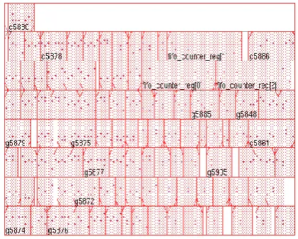
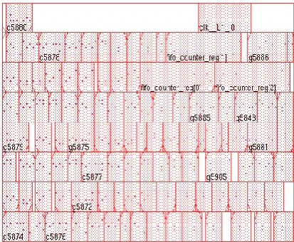
[image:3.595.322.533.566.735.2]In this paper, we specify a method to improve skew and delay in the design during clock tree synthesis. During physical implementation, comes the CTS (Clock Tree Synthesis) which is the process of insertion of buffers or inverters along the clock paths of ASIC design in order to achieve zero/minimum skew or balanced skew. The goal of CTS is to minimize skew and insertion delay. Clock is propagated after placement because the actual physical location of modules and cells are required for the clock’s propagation which in turn results in dealing with accurate delay and operating frequency. Values of skew, WNS, TNS and delay were observed and then the design was optimized in iterations. While buffers are inserted in the design, we resize them to get various values for WNS and TNS. Now, we select the buffer which gives maximum positive value for Worst negative slack (WNS) and total negative slack (TNS). If we get an optimum value for these slacks before optimizing the design for setup and hold conditions, we prefer using that buffer size. Now, on the basis of buffer selection, we observe the arrival times of various registers or cells used in the design. Based on the arrival time of the various registers, skew was calculated for different cells. Further, for improvement in clock delay values, the used buffer was relocated from its position and this was carried out in several iterations to get the minimum value for the clock delay. Figure 6 show the design before buffer insertion and figure 7 show the buffer insertion in the design.
Figure 7: Design after buffer insertion
4.
SIMULATIONS AND RESULTS
[image:4.595.63.270.70.240.2]With a design concept in mind, the RTL has been written in Verilog language. Verification of design was done and, it was required to synthesize the code in order to work further in the design implementation. The synthesized code generated the gate-level Netlist and the constraint file (.sdc) was exported which was further used in the next step of physical implementation which involved floorplanning, placement, routing and finally generation of GDS-II file. The simulation and synthesis of design was carried out on EDA tools. Table 1 shows the experimental results for percentage improvement in skew. Table 2 shows the experimental results on percentage improvement in delay.
Table 1: Improvement table for skew
Cell
Fan-out
Skew (ps)
Improvement in skew
(before) (after) (%)
DLY4X1 1 0.499 0.355 28.858
XNOR2XL 4 0.100 0.088 12.000
INVXL 4 0.241 0.210 12.863
OAI2BB1X1 3 0.186 0.140 24.731
AOI22XL 1 0.188 0.100 46.809
OAI211XL 1 0.569 0.423 25.659
DLY2X1 1 1.131 0.942 16.711
DLY4X1 1 0.000 0.000 0.000
[image:4.595.322.541.70.183.2]DFFRX1 1 0.000 0.000 0.000
Table 2: Improvement table for delay
Cell Delay
(ps)
Improvement in delay (before) (after) (%)
DLY4X1 1.438 1.348 6.259
XNOR2XL 0.499 0.389 22.044
INVXL 0.137 0.087 36.496
OAI2BB1X1 0.241 0.186 22.822
AOI22XL 0.186 0.148 20.430 OAI211XL 0.187 0.144 22.995
DLY2X1 0.570 0.483 15.263
DLY4X1 1.131 1.021 9.726
DFFRX1 0.000 0.000 0.000
5.
CONCLUSIONS
AND
FUTURE
SCOPE
For minimizing the clock skew a method of buffer insertion and resize is proposed i.e. clock skew was minimized during post-CTS timing analysis in physical implementation of the design. Also, buffer relocation method was used for minimizing the delay of the cells. Simulations were carried out on several EDA tools. As per the observation tables, we can see that overall skew was improved by 23.95% and delay is improved by 19.50% by buffer insertion, resizing and relocation. Further, the work can be extended for useful skew optimization.
6.
REFERENCES
[1] Weixiang Shena, Yici Cai, Wei Chen, Yongqiang Lu, Qiang Zhou and Jiang Hue, 2010, “Useful Clock Skew Optimization under A Multi-corner Multi-mode Design Framework,” in proceedings of 11th International Symposium on Quality Electronic Design (ISQED), 2010, pp. 62-68.
[2] Chiao-Ling Lung, Hai-Chi Hsiao, Zi-Yi Zeng, and Shih-Chieh Chang, “LP-Based Multi-Mode Multi-Corner Clock Skew Optimization,” in proceedings of International Symposium on VLSI Design Automation and Test (VLSI-DAT), April 2010, pp. 335-338.
[3] Haihua Su and Sachin S. Sapatnekar. “Hybrid structured clock network construction,” in Proceedings of the 2001 IEEE/ACM International Conference on Computer-aided design, pp. 333–336, 2001.
[4] Patrick Mahoney, Eric Fetzer, Bruce Doyle, and Sam Naffziger, “Clock distribution on a dual-core multithreaded Itanium-family processor,” in Digest of technical papers of the 2005 international solid-state circuits conference, pp. 292–293, 2005.
[5] R.-S. Tsay, “Exact zero skew,” In Proceedings of the 1991 IEEE international conference on Computer-aided design, pp. 336–339, 1991.
[6] Ting-Hai Chao, Yu-Chin Hsu, Jan-Ming Ho, and A.B. Kahng, “Zero skew clock routing with minimum wirelength,” Circuits and Systems II: Analog and Digital Signal Processing, Vol. 39, No. 11, pp. 799–814, Nov. 1992.
[7] Jason Cong, Andrew B. Kahng, Cheng-Kok Koh, and C.-W. Albert Tsao, “Bounded-skew clock and steiner routing,” ACM Transactions on Design Automatic Electronic System, Vol.3, No.3, 1998.
[8] Chung wen Albert Tsao and Cheng Kok Koh, “UST/DME: a clock tree router for general skew constraints” ACM Transactions on Design Automatic Electronic System, Vol. 7, No. 3, pp. 359–379, 2002.
[10] L.P.P.P. Van Ginneken, “Buffer placement in distributed RC-tree networks for minimal Elmore delay,” in proceedings of the IEEE International Symposium on Circuits and Systems, pp. 865–868, 1990.
[11] John Lillis, Chung-Kuan Cheng, and Ting-Ting Y. Lin, “Optimal wire sizing and buffer insertion for low power and a generalized delay model,” in proceedings of the 1995 IEEE/ACM international conference on Computer-aided design, pp. 138–143, 1995.
[12] Takumi Okamoto and Jason Cong, “Buffered Steiner tree construction with wire sizing for interconnect layout optimization,” in proceedings of the 1996 IEEE/ACM international conference on Computer-aided design, pp. 44–49, 1996.
[13] Charles J. Alpert, Anirudh Devgan, and Stephen T. Quay, “Buffer insertion with accurate gate and interconnect delay computation,” in proceedings of the 36th annual conference on Design automation, pp. 479–484, 1999.
[14] Y.-P. Chen and D. F. Wong, “An algorithm for zero-skew clock tree routing with buffer insertion,” in proceedings of the European Design and Test Conference, pp. 230–236, 1996.
[15] A. Vittal and M. Marek-Sadowska, “Power optimal buffered clock tree design,” in proceedings of the Design automation conference, pp. 230–236, 1996.
[16] I-Min Liu, Tan-Li Chou, Adnan Aziz, and D. F. Wong, “Zero-skew clock tree construction by simultaneous routing, wire sizing and buffer insertion,” in proceedings of the international symposium on Physical design, 2000, pp. 33–38, 2000.
[17] Hsiao-Pin Su, Wu, A.C.-H., Youn-Long Lin, “A timing-driven soft-macro placement and resynthesis method in interaction with chip floorplanning,” in proceedings of the 36th conference on Design automation, June 1999, pp. 262-267.
[18] Rony Kay, Gennady Bucheuv, and Lawrence T. Pileggi. EWA: exact wiring-sizing algorithm,” in proceedings of the International Symposium on Physical design, 1997, pp. 178–185.
[19] Jason Cong, Cheng-Kok Koh, and Kwok-Shing Leung, “Simultaneous buffer and wire sizing for performance and power optimization,” in proceedings of the 1996 international symposium on Low power electronics and design, 1996, pp. 271–276.
[20] Chung-Ping Chen, Chris C. N. Chu, and D. F. Wong, “Fast and exact simultaneous gate and wire sizing by lagrangian relaxation,” in proceedings of the 1998 IEEE/ACM international conference on Computer-aided design, 1998, pp. 617–624.
[21] Satyamurthy Pullela, Noel Menezes, and Lawrence T. Pillage, “Reliable non-zero skew clock trees using wire width optimization,” in proceedings of the 30th annual conference on Design automation, 1993, pp. 165–170.
[22] X. Zeng, D. Zhou, and Wei Li, “Buffer insertion for clock delay and skew minimization,” in proceedings of the 1999 international symposium on Physical design, 1999, pp. 36–41.
[23] Chung-Ping Chen, Yao-Wen Chang, and D. F. Wong, “Fast performance-driven optimization for buffered
clock trees based on lagrangian relaxation,” in proceedings of the 33rd annual conference on Design automation, 1996, pp. 405–408.
[24] Charles E. Leiserson, Flavio M. Rose, and James B. Saxe, “Optimizing synchronous circuitry by retiming,” In proceedings of the 3rd CalTech conference on Very Large Scale Integration, March 1983, pp. 87–116.
[26] L.W. Cotton, “Circuit implementation of high-speed pipeline systems,” in proceedings of the AFIPS Fall Joint Computer Conference, 1965, pp. 489–504.
[27] John P. Fishburn, “Clock skew optimization,” IEEE Transactions on Computers, July 1990, Vol. 39, No. 7, pp. 945–951.
[28] Rahul B. Deokar and Sachin S. Sapatnekar, “A graph-theoretic approach to clock skew optimization,” in proceedings of the 1994 IEEE International Symposium on Circuits and Systems, May 1995, Vol. 1, pp. 407–410.
[29] Jose Luis Neves and Eby G. Friedman, “Optimal clock skew scheduling tolerant to process variations,” in proceedings of the 33rd annual conference on Design automation, 1996, pp. 623–628.
[30] Ivan S. Kourtev and Eby G. Friedman. “Clock skew scheduling for improved reliability via quadratic programming,” in proceedings of the 1999 IEEE/ACM International Conference on Computer-aided design, 1999, pp. 239–243.
[31] Xun Liu, Marios C. Papaefthymiou, and Eby G. Friedman, “Maximizing performance by retiming and clock skew scheduling,” in proceedings of the 36th annual conference on Design automation, 1999, pp. 231– 236.
[32] Baris Taskin and Ivan S. Kourtev, “Performance optimization of single-phase level-sensitive circuits using time borrowing and non-zero clock skew,” in proceedings of the 8th ACM/IEEE international workshop on Timing issues in the specification and synthesis of digital systems, 2002, pp. 111–118.
[33] C. Albrecht, B. Korte, J. Schietke, and J. Vygen, “Cycle time and slack optimization for vlsi-chips,” in proceedings of the 1999 IEEE/ACM International Conference on Computer-aided design, pp. 232–238.
[34] Stephan Held, Bernhard Korte, Jens Maberg, Matthias Ringe, and J. Vygen, “Clock scheduling and clock tree construction for high performance ASICs,” in proceedings of the 2003 IEEE/ACM international conference on Computer-Aided design, 2003, pp. 232– 239.
[35] R. Bellman, “On a routing problem,” Quarterly of Applied Mathematics, 1958, Vol. 6, No.1, pp. 87–90.
[36] L. R. Ford and D. R. Fulkerson, “Flows in networks,” Princeton University Press, 1962.
[37] N. E. Young, Robert E. Tarjan, and J. B. Orlin, “Faster parametric shortest path and minimum-balance algorithms,” Networks, 1991, Vol. 21, pp. 205–221.
[38] Cadence’s “SOC Encounter RTL to GDSII System Datasheet” available on URL:
[39] Cadence’s “Encounter RTL Compiler Datasheet”
available on URL:
http://www.cadence.com/products/ld/rtl_compiler/pp./de fault.aspx
[40] Video Tutorial “Place and Route with Cadence SOC Encounter (Basics)” Online available at URL:http://www.youtube.com/watch?v=Z5WKIDbthdg.
[41] X. Zeng, D. Zhou, Wei Li, “Buffer Insertion for Clock Delay and Skew Minimization,” in proceedings of the International Symposium on Physical design, New York, 1999, pp. 36-41.
[42] Shih-Heng Tsai, Man-Yu Li, and Chung-Yang (Ric) Huang, 2012, “A Semi-Formal Min-Cost Buffer Insertion Technique Considering Mode Multi-Corner Timing Constraints,” in proceedings of 17th Asia and South Pacific Design Automation Conference (ASP-DAC), Feb 2012, pp. 505-510.
[43] Alessandro Balboni, Claudio Costi, Massimo Pellencin, Andrea Quadrini, and Donatella Sciuto, 1998, “Clock Skew Reduction in ASIC Logic Design: A Methodology for Clock Tree Management,” IEEE transactions on Computer-Aided Design of integrated circuits and systems, April 1998, Vol. 17, No. 4, pp. 344-356.
[44] N.Parthibhan, Mr.S.Ravi, and Dr. Kittur Harish Maillikarjun, 2012, “Clock Skew Optimization in Pre and Post CTS,” in proceedings of International Conference on Advances in Computing and Communications, Aug. 2012, pp. 146-149.
[45] Herr, Q.P., and Bunyk, P., 2003, “Implementation and application of first-in first-out buffers,” IEEE Transactions on Applied Superconductivity, June 2003, Vol. 13 , No. 2 , pp. 563-566.
[46] Xin Wang, Ahonen, T., and Nurmi, J., 2004, “A Synthesizable RTL Design of Asynchronous FIFO,” in Proceedings of International Symposium on System-on-Chip, Nov. 2004, pp.123-128.
ABOUT THE AUTHORS
Preeti Punia has done her Master of Technology (M.Tech) in VLSI Design from ITM University, Gurgaon (Haryana) India. She completed her B.Tech. in Electronics and communication
Engineering from Haryana College of Technology and Management affiliated to Kurukshetra University, Kurukshetra (Haryana) India. The area of her research interest includes RTL Design and Verification, Digital VLSI Design, EDA Tools Designing and Physical Design.
Rouble has done her M.Tech. in ECE (VLSI Design) from NIT Kurukshetra in 2013. She was a gold medalist of her batch during M.Tech. at NIT, Kurukshetra (2011-2013). She completed her B.Tech. in Electronics & Communication Engineering from DCRUS&T, Murthal, Sonepat (Haryana) in 2011 and is GATE qualified. She joined ITM University as Assistant Professor in January, 2014. The broad area of her research interest is VLSI Design including Digital IC Design, Semiconductor device characterization and modeling, Low power VLSI Design and Analog IC Design.
Neeraj Kr. Shukla (IETE, IE, IACSIT, IAENG, CSI, ISTE, VSI-India), an Associate Professor in the Department of Electrical, Electronics & Communication Engineering, and Project Manager – VLSI Design at ITM University, Gurgaon, (Haryana) India. He received his PhD from UK Technical University, Dehradun in Low-Power SRAM Design and M.Tech. (Electronics Engineering) and B.Tech. Electronics & Telecommunication Engineering) Degrees from the J.K. Institute of Applied Physics & Technology, University of Allahabad, Allahabad (Uttar Pradesh) India in the year of 1998 and 2000, respectively. He has more than 50 Publications in the Journals and Conferences of National and International repute. His main research interests are in Low-Power Digital VLSI Design and its Multimedia Applications, Digital Hardware Design, Open Source EDA, Scripting and their role in VLSI Design, and RTL Design.