International Journal of Computer Applications (0975 – 8887) Volume72– No.21, June 2013
Modeling and Simulation of 2D Mesh Topological
Network on Chip (NOC)
Prachi Agarwal
M.Tech Scholar, Department of Electronics, Institute of Engineering & Technology,
Alwar, Rajasthan India
Anil Kumar Sharma,
Ph.D Professor, Department ofElectronics, Institute of Engineering & Technology,
Alwar, Rajasthan India
Adesh Kumar
Assistant Professor, Department of Electronics Engineering, University of petroleum & Energy Studies,
Dehradun India
ABSTRACT
Network on chip (NOC) architecture is an approach to develop large and complex systems on a single chip. In this work, 2D mesh topological structure has been implemented in Very High Speed Integrated Circuit Hardware Description Language (VHDL). The architecture supports physical and architectural level design integration. Basic communication mechanism between resources is envisioned to be packet switched message passing through the switches. Node identification is done based on addresses of nodes located at X and Y axis. Network configuration is chosen for cluster 8 x 8 and 16 x 16 which signifies that 64 nodes and 256 nodes are available to communicate each other which are aligned in crossbar structure. Design was implemented in Xilinx 14.2 VHDL software, and functional simulation was carried out in Modelsim 10.1 b, student edition
General Terms
System on chip, Integrated circuits, Programming language
Keywords
Field Programmable Gate Array (FPGA). Network on chip (NOC), Very High Speed Integrated Circuit hardware Description language (VHDL
1.
INTRODUCTION
Integrated circuits contain several processor cores, memories, hardware cores and analog components on the same chip [1] [3]. Such Systems on Chip (SoC) [1] [4] [17] are widely used in high volume and high-end applications, such as multimedia, aerospace and defense, wired and wireless communication systems [10]. With the scaling in IC technology [6] more and more processors are integrating on a single die and formed a multiprocessor system on chip (MPSoC) [1] [8]. It results in the increase in the power consumption and wire delay [2]. In addition to this, with increased number of transistors and the die size, length of the interconnects [1] also increases. With reducing geometries, the wire pitch and cross section also reduces, thereby increasing the RC delay of the wires [2]. This coupled with increasing interconnect length leads to long timing delays on global wires. Another major impact of increased lengths and RC values is that the power consumption of global interconnects become significant, thereby posing a bigchallenge for system designers. Current on-chip interconnects [9] [18] consist of low-cost shared communication resources, where arbitration logic [9] is needed for the serialization of bus access requests: only one
master at a time can drive the bus. Major drawback of this solution is its lack of scalability [11] [18], which will result in unacceptable performance degradation (e.g, contention-related delays for bus accesses) when the level of SOC integration [12] will exceed a dozen of cores. Moreover, the connection of new blocks to a shared bus increases its associated load capacitance, resulting in more energy consuming bus transactions. Such factors make the on-chip communication among cores difficult. Therefore a scalable, energy-efficient on-chip interconnect network [8] is needed to address these difficulties in order to expedite the on-chip communication [3]. Network-on-Chip (NoC) [1] [2] [12] is a developing model used for VLSI systems implemented on a single integrated chip [12]. In a NOC system, modules such as microprocessor core, memory exchange [8] data and IP blocks with the help of a network called public subsystem [13] for the information traffic. A NOC is constructed from multiple data link and point to point interconnected by switches [7]. NOC utilizes the switching [11] [18] techniques. Connection is made in such a way that messages can be relayed from any source module to any destination module over several links, by making routing decisions at the switches [14]. These kinds of systems are used in the telephone exchanges [13] mobile communication [14] and topological networks [16] where fast data transfer is required in the real time environment.
2. 2D MESH NETWORK (8 x 8)
2D NOC follows the cross point technology which allows addressing any node at any time [11]. A cross point switch is a circuit switch having multiple inputs to multiple outputs in a matrix form. The 2D NOC architecture is a m × n mesh of switches [10] and resources are placed on the slots formed by the switches. For an m x n architecture there are m nodes on X axis and n nodes on Y axis respectively.
For the design and implementation of switching network [16], Considering a 8 x 8 architecture as shown in the figure 1. With the help of the network 64 nodes can be addressed and communicated at one time. To address 64 nodes 3 bits are required individually for the addresses of both axis (2n = 8). X_node_address has 3 bits address for X axis starting from 000 to 111 and Y_node_address has 3 bits address for Y axis starting from 000 to 111. Addressing and node selection scheme is described in the functional table 1. It is evident from Table 1 that if X_node_address is 000 and Y_node_address is 110, node n6 is selected. Similarly any node can be selected based on node address table having X_node_address and Y_node_address address.
Figure 1: Two dimensional (2D) cross point Topological (8 8) structure
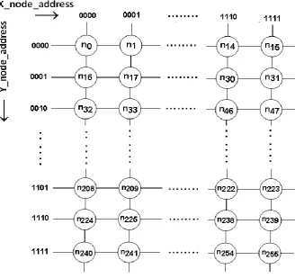
Figure 2: Two dimensional (2D) cross point Topological structure(16 x 16)
individually for the addresses of both axis (2n = 16). X_node_address has 4 bits address for X axis starting from
[image:2.595.135.464.386.695.2]International Journal of Computer Applications (0975 – 8887) Volume72– No.21, June 2013
[image:3.595.314.552.70.183.2]selection scheme is described in the functional table 2. It is evident from Table 2 that if X_node_address is 0001 and Y_node_address is 1110, node n30 is selected. Similarly any node can be selected based on node address table having X_node_address and Y_node_address address.
Table 1 Node Selection in 2D structure (8 x 8)
X_node_address Y_node_address Destination Node
000 000 Node 0
001 Node 1
010 Node 2
011 Node 3
100 Node 4
101 Node 5
110 Node 6
111 Node 7
001 000 Node 8
001 Node 9
010 Node10
011 Node11
100 Node12
101 Node13
110 Node14
111 Node15
010 000 Node16
001 Node17
010 Node18
011 Node19
100 Node20
101 Node21
110 Node22
111 Node23
011
000 Node24
001 Node25
010 Node26
011 Node27
100 Node28
101 Node29
110 Node30
111 Node31
100 000 Node32
001 Node33
010 Node34
011 Node35
100 Node36
101 Node37
110 Node38
111 Node39
101 000 Node40
001 Node41
010 Node42
011 Node43
100 Node44
101 Node45
110 Node46
111 Node47
110 000 Node48
001 Node49
010 Node50
011 Node51
100 Node52
101 Node53
110 Node54
111 Node55
111 000 Node56
001 Node57
010 Node58
011 Node59
100 Node60
101 Node61
110 Node62
111 Node63
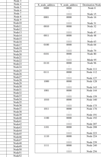
Table 2 Node Selection in 2D structure (16 x 16)
X_node_address Y_node_address Destination Node
0000 0000
: 1111
Node 0 : Node 15
0001 0000
: 1111
Node 16 : Node 31
0010 0000
: 1111
Node 32 : Node 47
0011 0000
: 1111
Node 48 : Node 63
0100 0000
: 1111
Node 64 : Node 79
0101 0000
: 1111
Node 80 : Mode 95
0110 0000
: 1111
Node 96 : Node 111
0111 0000
: 1111
Node 112 : Node 127
1000 0000
: 1111
Node 128 : Node 143
1001 0000
: 1111
Node 144 : Node 159
1010 0000
: 1111
Node 160 : Node 175
1011 0000
: 1111
Node 176 : Node 191
1100 0000
: 1111
Node 192 : Node 207
1101 0000
: 1111
Node 208 : Node 223
1110 0000
: 1111
Node 224 : Node 239
1111 0000
: 1111
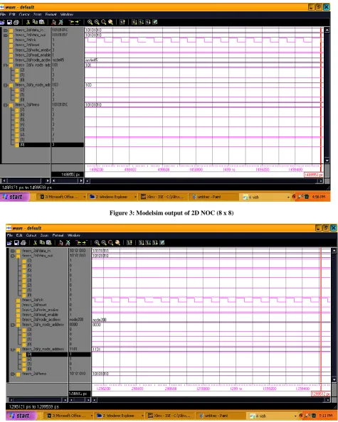
[image:3.595.189.539.201.742.2]Figure 3: Modelsim output of 2D NOC (8 x 8)
Figure 4: Modelsim output of 2D NOC (16 x 16)
3. SIMULATION AND RESULT
ANALYSIS
The work carries out the implementation of the chip for 2D 8 x 8 and 2D 16 x 16 Mesh Topological structures. It employs the cross bar structure. Traffic can be diverted to any node by their addresses. Time division multiplexing techniques is used
to detect the node which is applicable in telecommunication switching.
3.1 Tools Utilized
International Journal of Computer Applications (0975 – 8887) Volume72– No.21, June 2013
edition is a tool of Mentor Graphics Company used for simulation and debugging the functionality. The chip implementation is done using VHDL programming language.
3.2 Simulation Process sequence
Step 1: reset = 1, clk is used for synchronization and then run.
Step 2: reset = 0, same clk is used for synchronization and provide rising edge
Step 3: Select the address of destination node Node_address [5:0] of 6 bits for 8 x 8 structure and Node_address [7:0] of 8 bits for 16 x 16 structure.
Step 4: Force the value of X_node_address and Y_node_address of destination node. For 8 x 8 NOC X_node_address[2:0] and Y_node_address[2:0] are of 3 bits and for 16 x 16 NOC X_node_address[3:0] and Y_node_address[3:0] are of 4 bits.
Step 5: Give the eight bit value of data_in. Force write_en =1 and read_en =0 and then run.
Step 6: write_en =0 and read_en =1 and run. Desired output on destination is achieved.
When write_en =1 and read_en =0, the data is written in temp variable from the source node, when write_en =0 and read_en =1, the data is read from the temp variable to destination node. Clk is applied at the positive edge clock pulse and reset is kept at 1 for the initial state.
Figure 3 and 4 shows the simulated result for the 8 x 8 and 16 x 16, 2D NOC architecture.
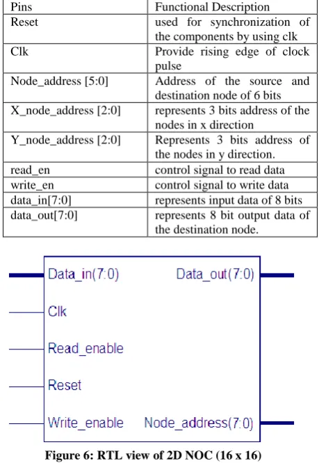
Register Transfer Logic (RTL) view of 8 x 8 and 16 x 16 NOC structure is shown in the figure 5 and 6. In both NOC structure, any node can be addressed and selected by its X_node_address and Y_node_address . Table 3 and 4 shows the pins details with the functional description of each pin for 8 x 8 and 16 x 16 NOC respectively.
[image:5.595.318.548.104.437.2]Figure 5: RTL view of 2D NOC (8 x 8)
Table 3 Design pins and their functional description for (8 x 8) NOC
Pins Functional Description
Reset used for synchronization of the components by using clk Clk Provide rising edge of clock
pulse
Node_address [5:0] Address of the source and destination node of 6 bits X_node_address [2:0] represents 3 bits address of the
nodes in x direction
Y_node_address [2:0] Represents 3 bits address of the nodes in y direction. read_en control signal to read data write_en control signal to write data data_in[7:0] represents input data of 8 bits data_out[7:0] represents 8 bit output data of
[image:5.595.63.271.434.594.2]the destination node.
[image:5.595.321.548.474.629.2]Figure 6: RTL view of 2D NOC (16 x 16)
Table 4 Design pins and their functional description for (8 x 8) and (16 x 16) NOC
Pins Functional Description
Reset used for synchronization of the components by using clk Clk Provide rising edge of clock
pulse
X_node_address [3:0] represents the 4 bit address of the nodes in x direction Y_node_address [3:0] Represents 4 bit address of the
nodes in y direction. read_en control signal to read data write_en control signal to write data data_in[7:0] represents input data of 8 bits data_out[7:0] Represents output data of 8
4. DEVICE UTILIZATION AND TIMING
SUMMARY FOR 2D NOC
Device utilization report gives the percentage utilization of device hardware for the chip implementation. Timing report generates minimum and maximum time to reach the output. Synthesis report extracted from the Xilinx shows the complete details of device utilization and timing summary.Selected Device: 2v40cs144-4, this device is targeted for FPGA. Device utilization summary for 8 x 8 and 16 x 16 2D Mesh NOC is shown in table 5.
Table 5 Device utilization in 2D structure
Device part Utilization
8 x 8 Structure 16 x 16 Structure Number of
Slices
14 out of 256 5 %
18 out of 256 7 %
Number of Slice Flip Flops
16 out of 512 3 %
20 out of 512 4 %
Number of 4 input LUTs
22 out of 512 4 %
25 out of 512 5 %
Number of bonded IOBs
27 out of 88 31 %
30 out of 88 34 %
Number of GCLKs
2 out of 16 12 %
2 out of 16 12 %
4.1 Timing Summary for 8 x 8 NOC
Timing details provides the information of delay, minimum period, minimum input arrival time before clock and maximum output required time after clock
Speed Grade: -4
Minimum period: 2.184ns (Maximum Frequency: 457.771MHz)
Mininput arrival time before clock: 4.735 ns Max output required time after clock: 5.38 6ns Total memory usage is 58820 kilobytes
4.2 Timing Summary for 16 x 16 NOC
Speed Grade: -4
Minimum period: 2.184ns (Maximum Frequency: 457.771MHz)
Minimum input arrival time before clock: 4. 935 ns Maximum output required time after clock: 5. 86 ns Total memory usage is 71466 kilobytes
Device utilization summary shows that there is 2 % change in number of slices, 1 % change in number of Slice Flip Flops, 1 % change in number of 4 input LUTs and Number of bonded IOBs when NOC cluster configuration changes from 8 x 8 to 16 x 16 NOC. There is very less change in the Minimum input arrival time before clock and Maximum output required time after clock but memory utilization change to 18 % because the number of nodes are increased.
5. CONCLUSION
Hardware chip implementation of the 2D, 8 x 8 and 16 x 16 mesh topological networks is carried out. The major advantage of the programmable structure is the identification of faulty node and replacement of it. A node can be found faulty by its crossbar address generation scheme on X and Y axis. Device utilization results shows that there is 2 % change in number of slices, 1 % change in number of Slice Flip Flops, 1 % change in number of 4 input LUTs and Number of
bonded IOBs when NOC cluster configuration changes from 8 x 8 to 16 x 16 NOC and memory utilization is 58820 kB and 71466 kB for both the networks respectively. 2D NOC architecture is found suitable for small area communication or LAN network but not in large area network. In the continuation of this work, a study can be carried out by taking into account the larger number of nodes. Addition of the features such as data security by encryption and decryption can be employed while data transfer among nodes. If we can add the network security algorithms along with the node data transfer, it will be suitable for long communication and wireless data networks.
6.REFERENCES
[1] Adesh Kumar, Sonal Singhal, Piyush Kuchhal “Network on Chip for 3D Mesh Structure with Enhanced Security Algorithm in HDL Environment ” International Journal of Computer Applications ( IJCA), USA, (ISBN: 973-93-80871-97-9) Volume 59– No.17 (page 6-13)
[2] David Atienzaa ,Federico Angiolini ,Srinivasan Murali , Antonio Pullinid, Luca Benini ,Giovanni De Micheli, Network-on-Chip design and synthesis outlook, INTEGRATION, the VLSI journal Elsevier 41 (2008) 340–359.
[3] D. Kim, Manho Kim, and G.E. Sobelman, “CDMA-based NoC architecture”, Proc. IEEE Conference on Circuits and Systems, vol. 1, pp. 137-140, 2004.
[4] Davide Bertozzi and Luca Benini, A Network-on-Chip Architecture for Gigascale Systems-on-Chip, IEEE Circuits and systems magazine, second quarter 2004, Xpipes, page (2-6)
[5] F. Karim A. Nguyen, and S. Dey, “An interconnect architecture for networking systems on chips”, IEEE Journal on Micro High Performance Interconnect, vol. 22, issue 5, pp. 36-45, Sept 2002.
[6] F. Angiolini, P. Meloni, S. Carta, L. Benini, L.Raffo, Contrasting a NoC and a traditional interconnect fabric with layout awareness, in: Proceedings of Design, Automation and Test in Europe Conference and Exhibition (DATE’06), Munich, Germany, ACM, IEEE Press, NewYork, 2006,pp.124–129.
[7] Jason Cong, Yuhui Huang, and Bo Yuan Computer Science Department University of California, Los Angeles Los Angeles, USA, 978-1-4577-1400-9/11/$26.00 ©2011 IEEE, A Tree-Based Topology Synthesis for On-Chip Network ,pp 2-6
[8] J. D. Owens, W. J. Dally etal., “Research challenges for on-chip inter connection networks,” IEEE MICRO, vol.27, no.5, pp.96–108,Oct.2007.
[9] Mohammad Ayoub Khan, Abdul Quaiyum Ansari, A Quadrant-XYZ Routing Algorithm for 3-D Asymmetric Torus Network-on-Chip, The Research Bulletin of Jordan ACM, ISSN: 2078-7952, Volume II (II) pp(18-26)
[10] M.Coppola, S.Curaba, M.Grammatikakis, R.Locatelli, G.Maruccia, F.Papariello, L.Pieralisi, White paper on OCCN: A Network-On-Chip Modeling and Simulation Framework, ISD Integrated system developments, page 8
International Journal of Computer Applications (0975 – 8887) Volume72– No.21, June 2013
and Engineering (IJSCE) ISSN: 2231-2307, Volume-1, Issue-6, January 2012, (page 1).
[12] P. Pratim Pande, C. Grecu, M. Jones, A. Ivanov, and R. Saleh, “Performance evaluation and design trade-offs for network-on-chip interconnect architectures”, IEEE Transactions on Computers, vol. 54, no. 8, pp. 1025-1040, 2005.
[13] Rikard Thid Thesis on “A Network on Chip Simulator”, Sweden Master of Science Thesis in Electronic System Design, Royal Institute of Technology Aug 2002, Page (9-27)
[14] S. Borkar, \design challenges of technology scaling." IEEE Micro, no.4, p. 2329, July-August 1999.
[15] V. Agarwal, M. Hrishikesh, S.Keckler, and D.Burger, \Clock rate versus ipc: the end of the road for conventional microarchitechtures, "in Proceeding of the 27th annual International Symposium on Computer Architrecture (ISCA'00'), vol.28, no.2, May2000, pp. 248
[16] Vitorde Paulo and Cristinel Ababei, 3D Network-on Chip Architectures Using Homogeneous Meshes and Heterogeneous Floorplans, Hindawi Publishing Corporation International Journal of Reconfigurable Computing Volume 2010, Article ID603059, 12 pages
[17] W. Wolf, The future of multiprocessor systems-on-chips, in: Proceedings of the 41st Design Automation Conference (DAC’04), June2004, pp. 681–685.
[18] Xin Wang and Jari Nurmi,Comparison of a Ring Chip Network and a Code-Division Multiple-Access On-Chip Network, Hindawi Publishing Corporation VLSI Design Volume2007,ArticleID 18372, 14 page
[19] W. Wolf, The future of multiprocessor systems-on-chips, in: Proceedings of the 41st Design Automation Conference (DAC’04), June2004, pp. 681–685.