Volume 71– No.12, May 2013
Voltage Sag Mitigation by using SVC
Tandra Sutradhar
Dept. of M.Tech ElectricalEngineering
Tripura University (A Central University)
Jhuma Rudra pal
Dept. of M.Tech ElectricalEngineering
Tripura University (A Central University)
Champa Nandi
Assistant Professor Dept. of Electrical EngineeringTripura University (A Central University)
ABSTRACT
This paper deals with modeling and simulation of SVC in IEEE 14 bus System with Induction Motor load for avoiding voltage sag. Single phase to ground fault is applied in predominant Induction motor load bus for voltage sag analysis. The effect of reactive power compensation to prevent sag has been analyzed with and without SVC.
Simulations of the SVC were carried out by using Power System Computer Aided Design (PSCAD) software. Simulation results prove that the SVC is capable of mitigating voltage sag with proper reactive Power support.
Keywords
SVC; Voltage sag; Voltage stability; Reactive power compensation
1.
INTRODUCTION
These days, high efficiency, maximum reliability, and security in the design and operation of power systems are more important than ever before. The difficulties in constructing new transmission lines due to limits in rights for their paths make it necessary to utilize the maximum capacity of existing transmission lines. Voltage sags associated with faults in transmission and distribution systems, energizing of transformers, and starting of large induction motor are considered as most important power quality disturbances (PQD) [11]. Voltage quality is worsened due to Voltage dips and interruptions caused by faults. These disturbances cause tripping of sensitive electronic equipments with disastrous consequences in industrial plants causing a complete stoppage of production. A momentary reduction of voltage magnitude relative to nominal or pre-event voltage magnitude and this can occur in any combination of phases. Voltage dip is characterized by minimum voltage magnitude and duration of dip event. The fact that the main duty of generation units is based on the active power generation requirements rather than the reactive power compensation makes the problem more serious. Flexible alternating current transmission system (FACTS) devices, as modern active and reactive power compensators, can be considered as viable and feasible options for satisfying the voltage security constraints in power systems, since their response to perturbations in urgent circumstances is fast, their performance in normal conditions is flexible, and their operation can fit the dynamic situations[1]. Its first concept was introduced by N.G.Hingorani in April 19, 1988. FACTS controllers are based on voltage source converters such as Static Var Compensators (SVCs), static Synchronous Compensators (STATCOMs), Thyristor Controlled Series Compensators (TCSCs), Static Synchronous Series Compensators (SSSCs) and Unified Power Flow Controllers (UPFCs). In recent years, new types of FACTS devices have been investigated that may
be used to increase power system operation flexibility and controllability, to enhance system stability and to achieve better utilization of existing power systems [2]. Today’s changing electric power systems create a growing need for flexibility, reliability, fast response and accuracy in the fields of electric power generation, transmission, distribution and consumption. Flexible Alternating Current Transmission Systems (FACTS) are new devices emanating from recent innovative technologies that are capable of altering voltage, phase angle and impedance at particular points in power systems. Their fast response offers a high potential for power system stability enhancement apart from steady state flow control. Static Var Compensator (SVC) provides more effective for providing fast-acting reactive power compensation. SVC also used for voltage regulation as well as reactive power compensation, dampen power swings and reduce system losses by optimized reactive power control. SVC is a shunt-connected static source or sink of reactive power [3]-[5], [9], [10]. In this paper investigate, voltage dip in a transmission line with and without SVC. SVC is placed in midpoint of a standard IEEE 14-bus system. A comparative performance evaluation with and without SVC has been studied. The proposed technique successfully improves the voltage dip in the power transmission systems.
2.
SVC
2.1
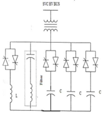
Thyristor switched capacitor
[image:1.595.339.513.517.712.2]-Thyristor controlled reactor (TSC-TCR)
Fig 1: Functional diagram of TSC-TCR.
Volume 71– No.12, May 2013 connected in parallel. The TSC branches are tuned with the
series reactor to different dominant harmonic frequencies. The main motivations in developing TSC-TCRs were for enhancing the operational flexibility of the compensator during large disturbances and for reducing the steady-state losses [6].
3.
OPERATING PRINCIPLE OF SVC
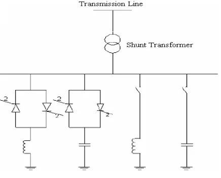
SVC is built up with reactors and capacitors, controlled by thyristor valves which are in parallel with a fixed capacitor bank. It is connected in shunt with the transmission line through a shunt transformer. Figure 2 and Figure 3 shows the equivalent circuit at which SVC is modeled. The model considers SVC as shunt-connected variable susceptance (Bsvc)
[image:2.595.320.541.187.320.2]which is adapted automatically to achieve the voltage control [7].
Fig 2: Functional diagram of SVC.
Fig 3: Equivalent circuit of SVC.
The current drawn by the SVC is
k svc
SVC
jB
V
I
(1)The reactive power drawn by the SVC, which is also the reactive power injected at bus k, is
SVC 2 K
SVC
Q
V
B
Q
(2)4.
VOLTAGE CONTROL BY THE SVC
The voltage-control action of the SVC can be explained through a simplified block representation of the SVC and power system, as shown in Figure 4. The power system is modeled as an equivalent voltage source (Vs), behind
equivalent system impedance (Xs), as viewed from the
SVC terminals. The system impedance Xs indeed corresponds
to the short-circuit MVA at the SVC bus and is obtained [6] as:
Fig 4: Simplified block representation of the SVC and power system.
u
.
p
in
MVA
.
S
V
X
bC 2 b S
(3)
Where,
C
S = 3-phase short circuit MVA at the SVC bus.
b
V = Base line to line voltage.
b
MVA = the base MVA of the system
If the SVC draws a reactive current ISVC, then in the absence
of the SVC voltage regulator, From the Phasor diagram the SVC bus voltage is given by
S SVC SVC
S
V
I
X
V
(4)
5.
CONTROL STRUCTURE
The block diagram of basic SVC Controller incorporating voltage regulator is shown in Figure 5. This shows that both voltage (VSVC) and current (ISVC) signals. The AC filter is
[image:2.595.55.273.245.420.2]Volume 71– No.12, May 2013
Fig 5: SVC Controller.
The rectified signal is filtered. The DC side filters include both a low pass filter (to remove the ripple content) and notch filters tuned to the fundamental and second harmonic components. The auxiliary signals mentioned in Figure 5, the outputs from the Susceptance (or reactive power) Regulator and Supplementary Modulation Controller. The Susceptance Regulator is aimed at regulating the output of SVC in steady state such that the full dynamic range is available during transient disturbances. The output of Susceptance Regulator modifies the voltage reference Vref in steady state. However
its operation is deliberately made slow such that it does not affect the voltage regulator function during transients [8].
The Gate Pulse Generation unit performs functions such as: • Ascertaining the number of TSC banks to be switched in order to meet the capacitive susceptance demand;
• Calculating the magnitude of TCR inductive susceptance in order to offset the surplus capacitive susceptance;
• Determining the order in which the TSC connections should be actuated, depending on the existing polarity of charges on the different capacitors, and hence ensuring transient-free capacitor switching;
• Computing the firing angle for TCR thyristors in order to implement the desired TCR inductive susceptance at the SVC terminals. As there is a highly non-linear relationship between the firing angle and the equivalent susceptance of the controlled reactors, a linearizing function is employed in the model in order to ensure that Bref is equal to BSVC, the actual
installed susceptance [6].
6.
SIMULATION AND DISCUSSION
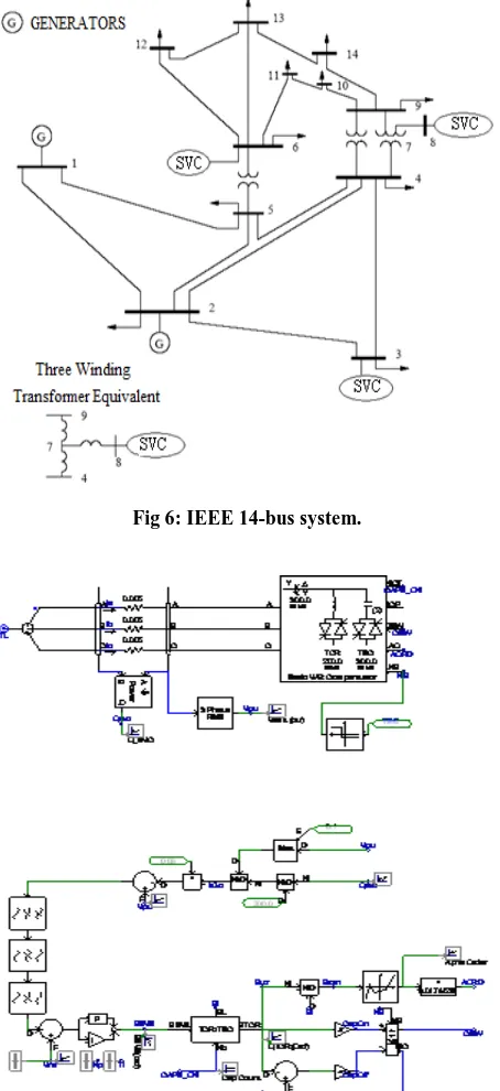
[image:3.595.316.543.74.569.2]A single line diagram of the IEEE 14-bus standard system is shown in Figure 6. In this system, three SVC is installed in BUS3, BUS6 and BUS8. There are 11 loads in the system. In this model we use two stations. Station 1 connected with bus1 and station 2 is connected to bus2. An Induction motor of 74.6KW is connected to bus 6 improving the power system performance. Fault is introduced into the system at a specific time. Here a 132 KV line is under simulation. Simulation design of SVC in PSCAD/EMTDC Environment is shown in Figure 7.
Fig 6: IEEE 14-bus system.
Fig 7: PSCAD representation of SVC with control system.
7.
Result and discussion of result
7.1
Voltage Sag due to Single line to
ground fault.
Volume 71– No.12, May 2013
Fig 7: Voltage characteristics graph (single phase to ground fault) of BUS 6.
7.2
SVC Reactive Power Compensation
The performance of reactive power compensation also depend on several factors such as load type, fault type, fault location. [image:4.595.57.541.337.529.2]The reactive power graph of SVC during faulty condition for .15sec (1sec to 1.15sec) in single phase is shown in figure bellow.
Fig 9: Reactive Power graph of SVC (Single phase to ground fault) of BUS 6.
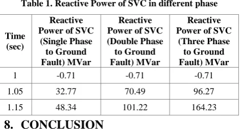
Table 1. Reactive Power of SVC in different phase
Time (sec)
Reactive Power of SVC
(Single Phase to Ground Fault) MVar
Reactive Power of SVC (Double Phase to Ground Fault) MVar
Reactive Power of SVC
(Three Phase to Ground Fault) MVar
1 -0.71 -0.71 -0.71
1.05 32.77 70.49 96.27
1.15 48.34 101.22 164.23
8.
CONCLUSION
This paper demonstrated that voltage dip condition with and without SVC. When SVC is use in the system then voltage dip case is avoided. When voltage is low SVC generate reactive power. The work aims at investigating the performance of the SVC for voltage regulation. Hence SVC is a promising device
9.
REFERENCES
[1] Mohsen GITIZADEH, Mohsen KALANTAR, Optimum allocation of FACTS devices in Fars Regional Electric Network using genetic algorithm based goal attainment’, Gitizadeh et al. / J Zhejiang Univ Sci A 2009 10(4):478-487, ISSN 1673-565X (Print); ISSN 1862-1775 (Online).
[2] Zhengyu Huang, Yixin Ni, C. M. Shen, Felix F. Wu, Shousun Chen, and Baolin Zhang, Application of Unified Power Flow Controller in Interconnected Power Systems—Modeling, Interface, Control Strategy, and Case Study, IEEE TRANSACTIONS ON POWER SYSTEMS, VOL. 15, NO. 2, MAY 2000.
[image:4.595.50.287.562.689.2]Volume 71– No.12, May 2013 [4] JIANG Tie-zheng, CHEN Chen, CAO Guo-yun,
Nonlinear optimal predictive controller for static var compensator to improve power system damping and to maintain voltage, Front. Electr. Electron. Eng. China (2006) 4: 380−384, DOI 10.1007/s11460-006-0073-5.
[5] Champa Nandi, Sumita Deb, Minakshi Deb Barma, and A.K. Chakraborty, Study and Simulation of the SVC and STATCOM Effect on Voltage Collapse and Critical Fault Clearing Time, International Journal of Modeling and Optimization, Vol. 2, No. 4, August 2012.
[6] R.Mohan Mathur and Rajib K. Varma, Thyristor_based FACTS Controllers for Electrical Transmission Systems, IEEE press 2002, A JOHN WILEY & SONS, INC. PUBLICATION, ISBN 0-471-20643-1.
[7] Enrique Acha,Claudio R. Fuerte-Esquivel, Hugo Ambriz-Pe´rez, Ce´sar Angeles-Camacho, FACTS Modelling and Simulation in Power Networks, Copyright ©2004 John Wiley & Sons Ltd, ISBN 0-470-85271-2.
[8] K.R.Padiyar, FACTS Controllers in Power Transmission and Distribution, Copyright © 2007, New Age International (P) Ltd., Publishers, ISBN (13): 978-81-224-2541-3.
[9] A.R. Boynuegri, B. Vural, A. Tascikaraoglu, M. Uzunoglu, R. Yumurtacı, Voltage regulation capability of a prototype Static VAr Compensator for wind applications, 0306-2619/$ - see front matter © 2011 Elsevier Ltd. All rights reserved. doi:10.1016/j.apenergy.2011.12.031.
[10]M. Gitizadeh, Allocation of multi-type FACTS devices using multi-objective genetic algorithm approach for power system reinforcement, Received: 24 February 2010 / Accepted: 28 September 2010 / Published online: 15 October 2010 © Springer-Verlag 2010.