Power and Area Efficient FLASH ADC Design using
65nm CMOS Technology
M.Abhilash Kumar
M.Tech,Dept of ECE MANIT,Bhopal
MP,India
Ajay kumar Dadoria
Ph.D,Dept of ECE MANIT,Bhopal
MP,India
Kavita khare,
Ph.DProfessor,Dept of ECE MANIT,Bhopal
MP,India
ABSTRACT
This paper presents a design of a high speed Comparator design using 65nm digital CMOS technology on Cadence Virtuoso Design Tool. The proposed FLASH ADC Design consists of fully differential topology. The first stage provides a Voltage Divider circuit and the second stage is Comparator Design having high sampling frequency tolerance, and the high efficient common drain circuit provides high driving capability with relatively low power dissipation. It is used in more application for bandwidth and power and a high resolution is available for analog-to-digital converters (ADCs). Under 1 V supply voltage, the simulation results show that the proposed FLASH ADC Design is having a differential topology along with latching circuit.
Keywords
Analog to Digital convertor(ADC), common mode feedback (CMFB) circuits, Complementary metal oxide semiconductor (CMOS),Voltage full scale range(VFSR), Differential non linearity (DNL), Least significant bit (LSB),Most significant bit (MSB),TSPCR(True Single-Phase Clock register).
1.
INTRODUCTION
As the CMOS technology is continuously scaling down, the design of ultra-high speed wired or wireless communication system is becoming possible. However, the advanced digital CMOS technology a challenging aspect for analog designers when designing mixed-signal systems. Operational amplifier, which is one of the key in analog modules, could achieve wider bandwidth due to the scaled transistor model, but when we consider a frequently decreased gain proportionally limited signal swing, poor synchronizing etc. For effectively increase operational amplifier’s gain and output voltage swing, multi-stage fully differential operational amplifier design is required. The operational amplifier with three or even more stages are cascaded with the Nested- Miller compensation or the Reversed Nested-Miller compensation that shows higher efficiency in the voltage gain enhancement, while they require additional large compensation capacitors compared to the basic two-stage operational amplifier, that will leads to a maximum die area and the limited slew rate [6][7].Besides, in addition to common mode feedback (CMFB) circuits, it would consume additional power. The traditional Comparator design using latching technique could provide adequate gain in Nano meter CMOS technology. Furthermore, for the high performance flash analog-to digital converter (ADC) in the Nanometer digital CMOS technology with low supply voltage, the requirements of high performance voltage divider bias circuit, the power efficient and high frequency samples tolerable comparator design and priority encoder deign along with latches. Targeting at the application in high performance ADCs, a Voltage divider circuit using CMOS Technology and a Comparator Design
using latching Technique is presented in this paper [4]. The proposed design enables this ADC to achieve a good resolution, high speed and high slew rate and keep the power dissipation low
2.
PRINCIPLE OPERATION OF FLASH
ADC
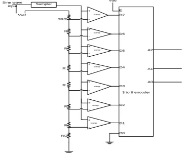
The 3-bit Flash ADC architecture as shown in Fig.1. The standard Flash ADC consists of three parts: The resistive network, the comparators, and the priority encoder along with latches [1]. Each comparator compares the voltage difference between its positive input from sampled sine wave VIN and its reference voltage as negative input from the Resistive ladder and then generates a digital output called thermometer code which is the output of comparator. The binary encoder generates corresponding 3-bit binary codes based on the comparator outputs. As shown in Fig.1. The encoder converts the thermometer code produced by the comparators to a binary code. As seen from the figure, the comparators all operate in parallel. Thus, the clock signal applied at a time for synchronization. Due to this, the conversion speed is limited .The speed of operation of FLASH ADC depends mainly on the speed of the comparator or the sampler. Due to this, the Flash ADC is capable of high conversion speed and doing operation for single clock pulse.
comp comp comp comp comp comp
Sampler Vref
comp
3 to 8 encoder Sine wave
input
D7
D6
D5
D4
D3
D2
D1 D0
A2
A1
A0 3R/2
R
R
R
R
R
R R/2
+
+
+
+
+
+
+
[image:1.595.340.522.494.645.2]
-E Vdd
3.
CONVENTIONAL WORK
0 0 0 0 0 d/dt 0 0 0 0 0 d/dt 0 0 0 0 0 d/dt 0 0 0 0 0 d/dt 0 0 0 0 0 0 0 0 0 0 0 0 0 0 0 0 0 0 0 0 0 0 0 0 0 0 0 0 0 0 0 0 0 0 0 0 0 0 0 0 Preamplifier ComparatorTSPCR EX-OR gate
[image:2.595.80.278.70.316.2]Fat tree encoder Latch + + + + -Vref Sine wave clock Bit n Bit n-1 Bit n-2 Bit 0
Fig 2: ADC Design
3.1
Resistive Averaging Technique:
Resistive averaging technique is often used in flash ADC, which can reduce the random offset of the preamplifiers and to reduce the nonlinearity of the ADC [8]. In order to improve the analysis on the effect to linearity (INL and DNL, it is useful to replace the pre-amplifier with a controlled voltage source with limited output impedance [9]. The voltage source is composed of three parts: the reference voltage input sampled sine wave and along with offset voltage applied at the input of the pre-amplifier. Therefore, by ignoring the nonlinearity of the amplifier, the superposition principle can be used to analyze the simplified linear circuit when the impact of reference voltage and input voltage are not taken into consideration.
3.2 Comparator Design
The schematic diagram of pre-latch comparator design having input stage of fully differential topology. In this design, two latches consisted of positive feedback to improve gain. The speed of the amplifier depends on recovery speed on latch circuit on M5-M8.All pMOS transistors and nMOS transistors having a proper width to achieve high driving capability. The total delay can be minimized with high gain and appropriate bandwidth. Applying a clock pulse ,as input voltage is more than the reference voltage ,output plus pin gives maximum pulse width depends on slew rate of the circuit).The output minus pin is complement to output plus pin signal. The TSPCR is used to generate clock to synchronize the comparator and encoder design.
[image:2.595.342.518.77.424.2]clk Sampled input vbias Vref m1 m2 m3 m4 m5 m6 m9 m7 m8 m10 m11 m12 m13 m14 Vdd Vdd Vdd Vdd gnd gnd gnd
Fig 3: Comparator Design
3.3
Fat Tree Coding
The encoder changes the thermometer code generated by comparators into binary code which is easy to understand, and there are mainly three suitable encoders to convert thermometer code into binary code for flash ADC. They are ROM/PLA, Fat Tree, and Wallace Tree. This design uses the Fat Tree encoder which is the fastest. First, change the thermometer code into one-hot code through Ex-OR gates, and then, change the one-hot code into binary code through Fat Tree encoder.
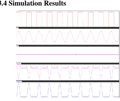
3.4
Simulation Results
[image:2.595.322.523.567.736.2]4.
PROPOSED WORK
4.1
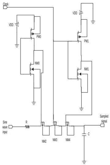
Sample and Hold Circuit
The sample and hold circuit of Fig:5 having a clock pulse. During the conducting phase of the switch, the signal on the capacitor charge up to the input signal, while in the quarantine (phase), the signal value remains fixed at its value at that moment of opening the switch. This moment is the theoretical sampling point in time. The T&H circuit can keep the signal at that level for a time period thus make allowable repeated use of the signal during the analog-to digital conversion. The track-and-hold switch is characterized by its on/off impedances. In a T&H circuit the on-resistance must be small and constant and the off impedance must be infinite. In the on-state the conductivity of a single MOS transistor as a switch depends on the MOSFET saturation voltage level. The dummy switches NM2 and NM4 as shown in Fig: 5 are single devices while the pass transistor NM3 consists of two parallel transistors for optimum cancellation. The control of the sample pulse edges requires careful balancing. If the “CLK” pulse switches off while the inverse clock pulse is not yet active, there will be a lot of switching glitches. If the inverse clock pulses become active while the “CLK” pulse is still active, the compensation charge will be supplied by the source and the whole method is ineffective. The occurrence of these two situations depends on the level of the input signal. The block box represents an inverter. The two pass transistors NM2 and NM4 having a width W/2 and the pass transistor NM3 in the middle having a width of W. The simulation results shown in Fig: 6.
Clock
VDD
VDD
Sine wave input
Sampled signal R
C PM0
PM1
NM0
NM1
[image:3.595.345.524.73.292.2]NM2 NM3 NM4
Fig 5: Sample ad Hold circuit immanent charge splitting
can be compensated by dummy switches
.
4.2
Voltage Divider Circuit
To obtain DC-bias voltages Vout0, Vout1, --- Voutn,
where Vss< Vout0 < Vout1 < ---VDD, voltage divider can be
used. Basically, resistive ladders are scarcely used in MOS Technology, mainly because of the large-die area required with suitable-values. Here, instead MOSFET‟s used in Totem pole configuration”.
Vref
Vout7
Vout6
Vout5
Vout4
Vout3
Vout2
Vout1
Vout0 NM8
NM7
NM6
NM5
NM4
NM3
NM2
NM1
NM0
[image:3.595.99.279.384.653.2]GND
Fig 6: Voltage divider circuit
The condition for saturation of nMOS device
Vds> Vgs-Vt---1
is satisfied.
Idc=K1 (W/L) NM0 (Vout0-Vt,NM0)2
=K1 (W/L)
NM1 (Vout1-Vt,NM1)2
=K1 (W/L)
NM2 (Vout2- Vout1-Vt,NM2)2
=K1 (W/L) NM2 (Vout2- Vout1-Vt,NM2)2 and so on
= K1 (W/L)
NM,n+1 (VDD- Vout,n - Vt,NM,n+1)2
Where K1 represents μn Cox
|VT | = |VT0| + γ { 2 |ϕp| + | VSB| )1/2 - ( 2 |ϕp| )1/2} (2)
Where γ (body effect coefficient)= {(2.q.NA ε si)1/2/ Cox}
q=electron charge(C).
ϕp=Fermi potential. (Positive for nMOS and negative for
pMOS.)
VSB=substrate bias voltage (V).
VT0=threshold voltage at zero body effect coefficient (V).
NA=charge concentration (carriers/cm 3
). μn= mobility of electrons (cm2/V-sec).
Cox= gate-oxide capacitance per unit area (F/m 2
).
In the above circuit, body bias effect is zero. If we consider the body bias effect the effect of threshold voltage is given as follows (assume Vss is ground terminal).
The Threshold voltages VT, NM0, VT.NM1--- are different
for different devices:
VT, NM0=VT.
|VT,NM1 | = |VT| + γ { 2 |ϕp| + | Vout0| )1/2 - ( 2 |ϕp| )1/2} (3) |VT,NM2 | =
|VT| + γ { 2 |ϕp| + | Vout1| )1/2 - ( 2 |ϕp| )1/2} (4) |VT,NM,n+1| = |VT| + γ { 2
4.3 Block Diagram of Comparator Design
Decision circuit
Post amplification
Preamplification
Vpositive
Vnegative
Iplus
Iminus
outplus
outminus
output
4.3.1 Specifications consider while designing
Comparator:
4.3.1.1
Offset Voltage
For an ideal op-amp, if non-inverting terminal and inverting terminal are equal, then output voltage is zero. In reality, this is not exactly true, and a voltage V0,off is not equal to zero
will occur at output for shorted inputs. Since, V0, off is
usually directly proportional to the gain of a circuit; the effect that can be more conveniently described in terms of the input offset voltage Vin,off , defined as the differential input voltage
needs to restore output voltage to zero in the practical devices[10,11].A resistive network as to be made to reduce offset voltage say offset compensation network.
4.3.1.2 Differential Nonlinearity
DNL error is defined as the difference between an real value step width and the ideal value of first LSB. For an ideal ADC, in which the differential nonlinearity coincides with DNL = zeroed LSB, for each analog step equals to 1LSB and the step values are spaced exactly 1LSB apart [12], here mostly N represents number of bits to indicate resolution of ADC. When its digital output increases (or remains constant) with an increasing input signal, by neglecting sign changes in the slope of the transfer curve.
LSB=(Vref)/2N
The voltage full scale range is calculated using the formula: Full sale=Vref-1LSB
4.3.1.3 Resolution:
Resolution is the smallest analog increment corresponding to a 1 LSB converter code change. For converters, resolution is normally expressed in bits, where the number of digital bits or codes which is equal to 2^n. As an example, an 8-bit ADC decodes the analog signal into 2^8 = 256 digital outputs .
4.3.1.4 Slew Rate:
Slew rate is defined as the change in output voltage with respect to time. i.e.,
Slew rate=(d/dt)Vo
For a sine wave output, the maximum slew rate occurs is equivalent to 2* Π*f*Vo,max .
4.3.1.5 Propagation delay:
The amount of time it takes the input signal with respect to reference voltage and simultaneously, the output changes from its state i.e., either logic ‘0’ or logic ‘1’.
Vref
Vin
Vout
tpLH
tpHL
tpLH is the delay time when the input switches and
crosses reference voltage Vref, that can make a
change the output from low to high.
tpHL is the delay time when the crosses reference
voltage, that can make a change the output from high to low.
The average of tpLH and tpHL gives the propagation
delay of comparator design. There are different aspects to reduce the propagation delay. The propagation delay normally varies with respect to amplitude of the input signal. Maximum amplitude of input signal will results a smaller delay time. Generally, the propagation delay can be reduced by cascading several stages of low gain amplifiers.
4.3.2 Pre amplification:
In order to improve the speed of the comparator and reduce the offset error caused by comparator, preamplifiers could be used. The Pre- amplification circuit is a CMOS differential amplifier consists of active loads. The transconductance sets the gain of an amplifier. The difference between the two inputs of the latch comparator would get bigger after the input signal amplified through the pre-amplifier. So, the latch comparator can compare faster. The design has used the low-gain, high bandwidth amplifier shown in Fig: 7 are cascaded, and the total delay can be minimized with high gain and appropriate bandwidth. The current mirror circuits are used as loading circuits i.e., PM0, PM2 and PM1, PM3.
Where gm,NM0=gm,NM1=gm.
I0++I0-=Iss.
4.3.3 Decision Circuit:
from the latch NM4 and NM5. The circuit makes a positive feedback by cross coupled NM4 and NM5 nMOS transistors say latching. To improve high driving capability based on mobility of charge carriers of holes and electrons, the width and length of pMOS and nMOS transistors are designed variable as shown in Table 1:
Vdd
Sampled signal
Vbias
Vref
outputplus
outputminus PM0
PM1
PM2
PM3
NM0 NM1
NM2
NM3 NM4 NM5
NM6
Vss
Vss
Vss
Preamplification
Decision circuit
I0+
I0+
I
0-I
0-Iss V0+
V0-PM7
[image:5.595.337.526.72.207.2]PM8
Fig 7: Comparator Design using 65nm CMOS
Technology using cadence tool.
When V0+>V0- :-
Vo+
Vo-I0+
I
0-NM3 NM4 NM5 NM6
Vss
Fig 8: Decision circuit
Vo+
Vo-I0+
I
0-NM3 NM5
[image:5.595.100.273.136.482.2]Vss
Fig 9: Equivalent circuit when V0+>V
0-Here,NM3 and NM5 are ON and NM4 and NM6 are OFF as shown in above figure 9.Here, all nMOS transistors having equal length and width. Under these circumstances, if V0+ is
equal to Vdd then V0- is equal to Vss.
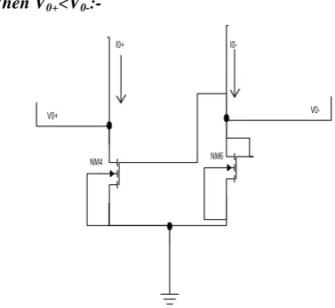
When V0+<V0-:-
V0+
V0-I0+
I0-NM4 NM6
Fig 10: Equivalent circuit when V0+<V0-
Here,NM4 and NM6 are ON and NM3 and NM5 are OFF as shown in above figure 10.Here, all nMOS transistors having equal length and width. Under these circumstances, if V0+ is
equal to Vss then V0- is equal to -Vdd.
V0+ V0+
r05
gm5V0+
Case 1:
Apply KCL law,
-I0+ + gm3 V0++ V0+/r03 =0 (1).
V0+[gm3+(1/r03)]=I0+
V0+=I0++[(1/gm3)//r03]
[image:5.595.326.515.291.464.2] [image:5.595.86.280.563.741.2]Here , I0+= I0+ because (W/L) of all nMOS are same. So, the
transconductance of NM3 and NM5 are as follows: gm3=µnCox(W/L)NM3(Vgs-Vt)
i.e., here gate and drain are shorted. So, the nMOS NM3 is always in saturation. Let us consider channel length modulation effect,
gm3=µnCox(W/L)NM3(Vgs-Vt)
gm3=µnCox(W/L)NM3(Vo+-Vt,NM3) (3)
V0+ V
0-r05
gm5V0+
Case 2
Similarly,gm5=µnCox(W/L)NM5(Vo+-Vt,NM5) (4)
Here, as applying body effect is zero, the threshold voltage of NM3 and NM5 should be same. So,
From equations [3] and [4] then., gm5= gm3
Hence, from above figure from case-2:
V0-=-gm5r05V0+ (5)
Zin,V0+=[V0+/ I0+]=(1/gm3)//r03 (6)
Zin,V0-=r05 (7)
Here, from equation (5),V0+=V0- with 180 0
phase shift.
4.3.4
Post amplification
Output Buffer:
In order to achieve high voltage gain along with limited input supply voltage, the output load must be as much as maximum. If such a stage is to navigate a low impedance load, then a source follower must be place after the decision making circuit to drive a load with negligible loss of the signal level i.e., the source follower can operate as a voltage buffer. In this proposed design the nonlinearity due to body effect can be eliminated by connected the body terminal or bulk is tied to the source terminal. The circuit diagram as shown in Figure 11:
c
outputplus
output minus
output Vdd
PM4 PM6
PM5
NM8 NM7
[image:6.595.336.516.73.251.2]NM9
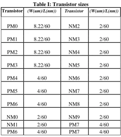
Fig 11: Common Drain schematic circuit Table I: Transistor sizes
Transistor (W(um)/L(nm)) Transistor (W(um)/L(nm))
PM0 8.22/60 NM2 2/60
PM1 8.22/60 NM3 2/60
PM2 8.22/60 NM4 2/60
PM3 8.22/60 NM5 2/60
PM4 4/60 NM6 2/60
PM5 4/60 NM7 2/60
PM6 4/60 NM8 2/60
NM0 2/60 NM9 2/60
NM1 2/60 PM7 4/60
PM6 4/60 PM7 4/60
4.4
Encoder Design
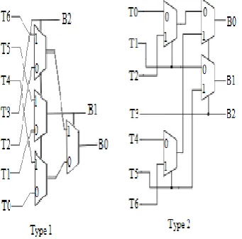
Multiplexer is the building block of the decoding section. The Flash ADC is implemented using Thermometer code itself as select line because of considering speed and power consumption. The design are implemented using multiplexer 2*1.Here, each box is 2*1 mux. It offers better decoding speed and minimum power consumption compared to Fat Tree based decoder.2x1 multiplexers connected as a tree constitutes the decoder structure. These decoders provide a short critical path and small area. Depending upon the method of implementation of truth table, multiplexer (MUX) based decoder is of two types. First type of decoder uses output Binary code as multiplexer select lines and the second one uses thermometer code as select lines.
[image:6.595.328.531.275.504.2]Fig 12: encoder design using2*1 mux with both types of select lines
5.
SIMULATION RESULTS
[image:7.595.106.277.88.256.2]5.1
Sample and Hold circuit
Fig 13: Sample and Hold Circuit of sampling frequency of 20M samples per sec
[image:7.595.332.524.122.423.2]5.2
Comparator Design
Fig 14: Comparator design using Cadence 65nm CMOS Technology
5.3
Output of FLASH ADC
[image:7.595.103.276.316.527.2]Fig 14: Output of FLASH ADC using transient analysis with input as pulse signal
Fig 15: Output of FLASH ADC using transient analysis with input as sinusoidal signal
6.
COMPARISON RESULTS
Performance Summary
Parameters
Conventional
work Proposed work
Technology 180nm CMOS 65nm CMOS Resolution 7 bit 3 bit Max.Sampling
rate 1GS/s 1GS/s
Supply voltage 900mv 0.65-1 volt Input range 280mV(p-p) 280mV(p-p)
Input Frequency(ma
x) 97.8MHz 1G Hz
Offset
Voltage(mV) 196.81 225.36 Slew rate .256(V/µsec) 75.59(V/µsec)
Power
consumption 494.2mW 249.5mW
LSB 7.87mV 28.7mV
DNL -0.1 to +0.1 LSB
~0.5 to 0.5 LSB Propagation
[image:7.595.84.277.562.722.2]7.
CONCLUSION
The proposed circuit is tested and verified in various aspects. The speed, resolution, supply voltage and clock frequency are considered. The circuit is able to resolve small difference in voltage as low as 5m volts when operating at 1V input power supply voltage, with clock frequency of more than 600MHz using cadence virtuoso on 65nm CMOS Technology. This circuit can be widely used in ADC, when ever speed is required.
8.
FUTURE WORK
In order to continue our work on removal of offset voltage in comparator design and a sampler circuit design to work on GIGA samples per sec and to increase a high driving capability of sampling circuit and comparator design and Fat tree encoding to improve speed of Flash ADC design .The future work is switches to Bi-CMOS Technology.
9.
REFERENCES
[1] J. Ceballos, I. Galton, and G. Temes, “Stochastic analog-to digital conversion,” in Proc. 48th Midwest Symp. Circuits and Systems, Aug.2005, pp. 855 858. [2] “Analog MOS Integrated circuits for Signal
Processing”, by Roubik Greegorian,Gabor C.TEMES.
[3] Amalan Nag, K. L. Baishnab F. A. Talukdar, Member, IEEE ”Low Power, High Precision and Reduced Size CMOS Comparator for High Speed ADC Design” 2010 5th International Conference on Industrial and Information Systems, ICIIS 2010, Jul 29 - Aug 01, 2010, India.
[4] T. Sundsröm and A. Alvandpour, “Utilizing Process variations for reference generation in a flash ADC,” IEEE Trans. Circuits Syst. II,vol.56, pp. 364–368,May 2009.
[5] “Design of Analog CMOS Integrated Circuits”, by Behzad Razavi, Tata McGraw Hill Edition 2002, ISBN – 0- 07-238032-2.
[6] K.N. Leung, P.K.T. Mok, “Analysis of Multistage amplifier frequency compensation”, IEEE Trans.Circuits Systems I: Fund. Theory 48 (9) (2001) 1041- 1056. [7] B.K. Ahuja, “An improved frequency compensation
technique for CMOS operational amplifiers”, IEEE J. Solid- State Circuits 18 (1983) 629–633.
[8] K.Kattmann and J.Barrow, “A technique for reducing differential non-linearity errors in flash A/D converters”,in Proc.IEEE Int.Solid-State Circuits Conf.1991, pp.170–171.
[9] P.C.S.Scholtens and M.Vertregt,"A 6-b 1.6 Gsamples/s flash ADC in 0.18um CMOS using averaging termination,"IEEE J.Solid-State Circuits, vol.37, no.12, pp.1599-1609, Mar.2002.
[10] Hank Zumbahlen, Basic Linear Design, Analog Devices, 2006, ISBN: 0-915550-28-1.Also available as Linear Circuit Design Handbook, Elsevier-Newnes, 2008, ISBN-10: 0750687037,ISBN-13: 978-0750687034.Chapter1.
[11] Walter G. Jung, Op Amp Applications, Analog Devices, 2002, ISBN 0-916550-26-5, Also available as Op Amp Applications Handbook, Elsevier/Newnes, 2005, ISBN 0-7506-7844-5. Chapter 1.
[12] INL and DNL definitions "A DNL error specification of less than or equal to 1LSB guarantees a monotonic transfer function with no missing codes. http://www.maxim-ic.com/app-notes/index.mvp/id/283. [13] Erik Sail, Mark Vesterbacka , “A multiplexer based