preliminary version 1.3
Copyright (C) 1986 by Digital Equipment Corporation
CHAPTER 1 1.1 1.2 1.3 1.4 1.4.1 1.4.2 1.4.2.1 1.5 1.6 1.7 1.8 CHAPTER 2
2.1 2.2 2.2.1 2.2.2 2.2.3 2.2.4 2.2.5 2.2.6 2.2.7 2.2.8 2.2.9 2.2.10 2.2.11 2.2.12 2.2.13 2.2.14 2.2.15 2.3 2.4 2.4.1 2.5 2.5.1 2.5.2 2.5.3 2.6 2.7 CHAPTER 3
3.1 3.2 3.2.1 3.2.2 CONTENTS OVERVIEW
• 1-1 INTRODUCTION • • • • . • • •
KXJ11-CA HARDWARE FEATURES . . OPERATIONAL OV~RVIEW ( ••••• ) •
. . . . . . 1-1
· . . . . 1- 3
KXJ11-CA OPERA~ING MODES • 1-3
Standalone Mode . . . . . . 1-3 lOP Mode • • • • . •
KXJ11-CA Fro~ Point Of
. . . 1- 4 View Of Arbiter.. . 1-4 SOFTWARE ENVIRdNMENT . •
KXJII-CA SPECIFICATIONS TERMINOLOGY US~D IN THIS RELATED DOCUMENTS
· . . . . . . . 1 ... 4 · . . . . . . 1-4 DOCUMENT • • • • • . 1-5
· . . . . 1-6
INSTALLATION
INTRODUCTION • '. • • • • • • • • • • • • 2-1 . . • 2-1 SELECTING OPERATING FEATURES . . . •
• • • • • • 2-- 4
. • 2-8 Boot/Self test-Switch • • • •
Q-Bus Size • • • . • Q-Bus Base Address Selection DMA Requests • • • • • .
. . . 2-9 BREAK Enable • • • • • . • • . • . • • • •
HALT Option Selection Power-Up Option Selection PROM Addressing • • • • • SLU1 Baud Rate . . . . SLU1 Transmitter . . .
SLU1 Receiver . . . • . • SLU2 Channel A Receiver . • • • . . • • • • . SLU2 Channel
e
Transmitter . • • • • • • • • SLU2 Channele
Receiver . • • .2-11 2-12 2-13 2-14 2-15 2-16 2-17' 2-18 2-19 2-20 2-23 Real-Time Cloqk Interrupt
POWER SUPPLY CONSIDERATIONS . . . • INSTALLING THE ~XJ11-CA INTO A BACKPLANE
-2-24 · • . • 2-25 2-26 Edge Connecto~ Pin Assignments • • • . 2-27 CONNECTORS AND EXTERNAL CABLING
Parallel I/O Interface (J4) Serial I/O Lines (J1, J2, J3)
. • • • • • 2-30 · . . • . 2-30 Loopback Connectors . • . . . • .
2-31 2-37 2-38 2-39 ERROR DETECTION ;AND REPORTING WITH THE LEDS
DIAGNOSTIC TES~tNG WITH XXDP+ ARCHITECTURE
INTRODUCTION . • • . . . . • • • • . KXJ11-CA BLOCK DIAGRAM
J-11 Microprocessor . • . . • • • •
RAM • • • • • • '. •
3.2.3 Two Port Register (TPR) File • • • • • • 3 • 2 • 3 • 1 TPRO • ~ • • • • • • • • • • • • • • 3.2.3.1.1 TPRO As A Control Register • • • • • • • • • 3.2.3.1.2 TPRO As A Test Register • • • • • • • • • • • 3.2.3.1.3 TPRO As A Q-Sus OOT Register • • • • • • • • 3 • 2 • 3 • 2 TPRl • • • • • • • • • • • • • • • • • • 3 • 2 • 3 • 3 TPR2 • • • • • • • • • • • • • • • • • • 3 • 2 • 3 • 4 TPR3 • • • • • • • • • • • • • • c o . • •
3.2.3.5 TPR4 Through TPR15 • • • • • • • • • 0 "
3.2.4 CPU 10 Switch • • • • • • • • • • • • • • • •
3.2.5 DNA Controller • • • • • • • • • • • • • • •
3.2.6 Wake-up Circuit • • • • • • • • • • • • • • •
3.2.7 PROM And Firmware Control • • • • • • • • • •
3.2.7.1 Native F~rmware Vs. User-Designed Firmware
3.2.8 KXJll-CA Control And Status Registers • • • •
3.2.8.1 KXJll Control/Status Register A (KXJCSRA) • • 3.2.8.2 KXJ11 Control/Status Register B (KXJCSRB) • • 3.2.8.3 KXJll Contr~l/Status_ Register C (KXJCSRC) • • 3.2.8.4 KXJ11 Control/Status Register D (KXJCSRD) • • 3.2.8.5 KXJ11 Control/Status Register E (KXJCSRE) • • 3.2.8.6 KXJl1 Control/Status Register F (KXJCSRF) • • 3.2.8.7 KXJ11 Control/Status Register H (KXJCSRH) • • 3.2.8.8 KXJ11 Control/Status Register J. (KXJCSRJ) • •
3.2.9 Q-Sus Interrupt Register (QIR) • • • • • • • •
3.2.10 Maintenance Register • • • • • • • • • • • •
3.2.11 Program Interrupt Request (PIRQ) Register • •
3.2.12 CPU Error Register • • • • • • • • • • • • •
3.2.13 Processor Status Word (PSW) • • • • • • • • •
3.2.14 Console Asynchronous Serial I/O • • • • •
3.2.15 Synchronous/Asynchronous Serial I/O • • •
3.2.16 Parallel I/O • • • • • • • • • • • • • • • •
3.2.17 -12V Charge Pump • • • • • • • • • • • •
3.3 Q-BUS INTERFACE • • • • • • • • • • • • • • • • 3.4 TWO-PORT REGISTERS AND COMMUNICATION WITH THE 3.5 3.5.1 3.5.2 3.5.3 3.6 3.1 3.7.1 3.7.2 3.8 3.8.1 3.8.2 3.8.3 3.8 .. 4
3.8.5 3.8.6 3.9 3.9.1 3.9.2 3.9.3 3.9.4
ARB ITER • . • • • • • • ., • . • • • • • • • • • KXJ11-CA INTERRUPTS • • • • • • • • • • • • • • ~ Interrupts From The Q-Bus To The KXJl1-CA • • Interrupts From The KXJl1-CA To The Q-Bus • • Local Interrupts From On-Board Devices • • • SPECIAL INTERRUPT HANDLING . . . . , . . . KXJ11-CA RESETS • • • • • • • • • • • • • •
Software Reset • • • • • . • • • • • • • • • • • Hardware Reset • • • • • • • • • • • • • • • •
MEMORY MANAGEMENT ARCH I TECTURE • • • • • • • • •
Page Address Registers (PARs) • • • • • • Page Descriptor Registers (PDRs) • • • • • • Memory Management Register 0 (MMRO) • • • •
Memory Management Register 1 (MMR1) co • . , .
Memory Management Register 2 (MMR2) ., •
Memory Management Register 3 (MMR3) • • • •
SHARED MEMORY • • • • • • • • • • • • • • •
Shared Memory Organization • • • • • • • • • Defining One Block Of Shared Memory • • •
Defining Two Blocks Of Shared Memory • •
Defining 64 Blocks Of Shared Memory • • • • •
3.9.5 3.9.6
CHAPTER 4 4.1 4.2 4.3 4.3.1 4.3.1.1 4.3.1.2 4.3.2 4.3.2.1 4.3.2.2 4.3.2.3 4.3.2.4 4.3.2.5 4.3.2.6 4.3.2.7 4.3.2.8 4.4 4.4.1 4.4.2 4.4.3 4.4.4
\..riAPTER 5 5.1 5.2 5.2.1 5.2.1.1 5.2.1.2 5.2.2 !5.2.2.1 !5.2.2.2 5.2.2.3
5.i:3
~).2.3.1 5.2.3.2 5.2.3.3 5.2.4 5.2.4.1 5.2.4.2 5.2.4.3 ~;.2.5 ~;.2.65.2.6.1 "'-5.2.6".2 5.2.6.3
Enabling And D'isabling Shared Memory Shared Memory Considerations • • • •
DNA TRANSFER CONTROLLER (DTC)
. .
.
.
.
.
Page 3
3-50 3-52
OVERVI EW • • • • • • • • • • • • • • • • • • • • • 4-i
DTC CONSIDERATIONS • • • • • • • • • • • • • • • • 4-2 DATA TRANSFER CONTROLLER (DTC) REGISTERS • • • • 4-2
DTC Global Registers • • • • • • • • • • • • • 4-4
Command Register • • • • • • • • • • • • • • • 4-4
Master Mode Register • • • • • • • • • • • 4-6
DTC Channel ~e9isters • • • • . • • • • • 4-7
Current Address Registers A And B • • • • • •• 4-7 Base Address Registers A And B • • • • • • • • 4-9 Chain Address Register • • • • • • • • • • • • • 4-9 Interrupt Vector And Interrupt Save Register 4-10 Status Register • • • • • • • • • • • • • • • 4-12
Current And Base Operation Count Registers 4-14
Pattern And Mask Registers • • • • • 4-14
Channel Mode Register • • • • • • • • 4-15
PROGRAMMING THE DTC • • • • • • • • • • • • • • 4-18 Chip Initialization • • • • • • • • • • • • • 4-18 Data Transfer • • • • • • • • • • • • • • •• 4-21
Termination Options • • • • • • • • • 4-22
Examples • • • • • • • • • • • • • • • • • •• 4-22
PARALLEL I/O CONTROLLER (PIO)
OVERVIEW • • • • • • • • • • • • • • • • • • • • 5-1
PARALLEL I/O PORT (PIa) REGISTERS • • • • • • • • 5-2
Master Control Registers • • • • • • • • • • • 5-4
Master Interrupt Control Register • • • • • • • 5-4 Master Configutation Control Register • • • • • 5-5
Port Specification Registers • • • • • • • • • 5-7
Port Mode Specification Registers (Ports A And
B) • • • • • • • • • • • • • • • • • • • • • • • 5-7 Port Handshake Specification Registers (Ports A And B) • • • • • • • • • • • • • • • • • • • • • 5-9 Port Command And Status Registers (Ports A And
B) • • • • • • • • • • • • • • • • • 5-11
Bit Path" Definition Registers • • • 5-12
Data Path Polarity Registers •• •• 5-13
Data Direction Registers • • • • • 5-13
Special I/O.Control Registers • • • • 5-14
Pattern Definition Registers • • • • 5-15
Pattern Polarity Registers (PPR) • • •• 5-15
Pattern Transition Registers (PTR) • • • 5-16
Pattern Mask Registers (PMR) • • • • • • 5-16
Port Data Registers • ...-. • • • • • • 5-16 PIO Counter/Timer Control Registers . • • • • • 5-17
PIa Counter/Timer Mode Specification 5-17
PIa Counter/Timer Command And Status • • • • 5-19
PIO Counter/Timer Current Count • • • • • • • Interrupt Related Registers • • • • • • • • • Interrupt Vector Register • • • • • • • • • • Current Vector Register • • • • • • • • • • • I/O Buffer Control Register • • • • • • • • • 5.2.6.4 5.2.7 5.2.7.1 5.2.7.2 5.2.8 5.3 5.3.1 5.3.2
PROGRAMMING THE I/O PORTS • • • • • • • • • • • Programming The I/O Ports As Bit Ports • • • • Programming The I/O Ports As Ports With
5-21 5-22 5-22 5-23 5-23 5-24 5-25 5.3.2.1 5.3.2.2 5.3.2.3 5.3.2.4 5.3.2.5 5.3.2.6 5.3.3
Handshake • • • • • • • 0 • • • • • • • • Example • • • • • • • • • • • • • • • • • • • Example • • • • • • • • • • • • • • • • • Example • • • • • • • • • • • • • • • Example • • • • • • • • • • • • • • • • Example • • • • • • • • • •
Example • • • • • • • • • • • • • • • • • PROGRAMMING THE PIO COUNTER/TIMERS • • • • • •
5-27 5-33 5-36 5-38 5-40 5-41 5-43 5-44
CHAPTER 6 SERIAL LINE UNITS (SLUS)
6.1 OVERVIEW • • • • • • . • • • • • • • • • • • • • • 6-1 6.2 6.2.1 6.2.1.1 6.2.1.2 6.2.1.3 6.2.1.4 6.2.2 6.3 6.3.1
CONSOLE SERIAL PORT (SLUl) • • • • • • • • • • • 6-1
SLU1 (Console) Reg isters ...~ 6-2
Receiver Control/Status Register (ReSR) • • • • 6-2 Receiver Buffer Register (RBUP) • • • • • • • • 6-3 Transmitter Control/Status Register (XCSR) • • • 6-4 Transmitter Buffer Register (XBUP) • • • • • • 6-5 Examples • • • • • • • • • • • • • • • • • • • • 6-6 MULTIPROTOCOL SERIAL CONTROLLER (SLU2) • • • • • • 6-6
Synchronous/Asynchronous Serial Line (SLU2) 6.3.1.1
6.3.1.2 6.3.1.2.1 6.3.1.2.2 . 6.3.1.3
6.3.1.3.1 6.3.1.3.2 6.3.1.3.3 6.3.1.3.4 6.3.1.3.5 6.3.1.3.6 6.3.1.3.7 6.3.1.3.8 6.3.1.3.9 6.3.i.4 6.3.1.4.1 6.3.1.4.2 6.3.1.4.3 6.3.1.5 6.3.1.6 6.3.2
Registers • • • • • • • • • • • • • • • • • • • 6-7 KXJ11 Control/Status Register A (KXJCSRA) • • • 6-8 Time r Reg is t e r s • • • • • • • • • • • • • • . • • 6 - 9
SLU2 Timer Control Registers • • 6-10
SLU2 Timer Data Registers • • • • • • • • 6-12
SLU2 Control Registers • • • • • • • e . 6-14
Control Register 0 • • • • • • • • • • • • • 6-14
Control Register 1 • • • • • • • 6-17
Control Register 2 - Channel A • • • • • • • 6-19
Control Register 2 - Channel B • • • • • 6-20
Control Register 3 • • • • • • • • • • • • • • 6-21 Control Register 4 • • • • • • • • • • • • • • 6-23· Control Register 5 • • • • • • • • • • 6-25 Control Register 6 • • • • • • • • • • • • 6-26 Control Register 7 • • • • • • • • • • 6-26
SLU2 Status Registers • • • • • • • • 6-27
Status Register 0 • • • • • • 6-27
Status Register 1 • • • • • • • • • • • • • • 6-29
Status Register 2 (Channel B Only) • • 6-31
SLU2 Transmitter Registers • • • • • • • • • 6-31
SLU2 Receiver Registers • • • • • • • • • 6-32
APPENDIX A A.l
APPENDI:X B B.l
Page 5
MEMORY MAP SUMMARY
REGISTER SUMMARY
. .
.
. .
.
• • • • • • • • • • A-lKXJll-CA/KXTll-CA DIFFERENCES
1 • 1. I NTRODUCT I ON
OVERVIEW
The KXJll-CA (M7616) is an I/O processor based on the J-ll
microprocessor chip. It is a quad-height, extended length,
single-width module that executes the extended PDP-ll instruction set
(all 140 instructions including floating-point) with memory.
management. The KXJ11-CA can operate as a Q-Bus slave device under the direction of a Q-Bus arbiter processor or can act as a st.andalone processor.
The KXJll-CA meets the spec~fication for a Q-Bus slave and Q-Bus DNA master and can interface w~th most of Digital's large family of Q-Bus modules described in the Mic;rocomputer Interfaces Handbook and the Microcomputers and Memories Handbook.
1.2 KXJ11-CA HARDWARE FEATURES
The KXJ11-CA has the following features:
0-. J-l1 (DCJ1l-AC) l6-bi t microprocessor
Executes extended PDP-ll instruction set (140 instructions
including floating-point).
Contains memory management unit for three levels of memory protection and 4 MBaddressing.
Operates at 14
MHz.
o Memory
512 KB of dynamic RAM
Can be accessed by local (on-board) devices and Q-Bus devices
KXJll-CA User's Guide
OVERVIEW PRELIMINARY 4/3/86
Up to 64 KB of PROM; 16 KS of whichris for firmware
o Q-Bus interface
16 word, two-ported RAM (TPR) register file for passing
commands and parameters.
Mechanism for posting interrupts to the Q-Bus.
o Two channel pt:ogrammable DMA transfer controller (DTC)
Performs transfers between local 22-bit addresses and I6-bit, 18-bit, or 22-bit Q-Bus addresses.
'0 Eight control/status registers
o Console asynchronous serial line
DL-compatible
- 'EIA RS-422/RS-423/RS-232C compatible
Programmable baud rates of 300 to 38400
o Primary synchronous/asynchronous serial line unit
Full modem support
EIA RS-449 (CCITT V.24) and RS-422/RS-423/RS-232C compatible
Programmable baud rates of 110 to 76800
Bit-oriented or
support character-oriented synchronous
o Secondary synchronous/asynchronous serial line unit
RS-449 <CCITT V.24) data and timing only
RS-422/RS-423/RS-232C compatible
Programmable baud rates of 110 to 76800
Bit-oriented or character-oriented synchronous
support
Party line operation
protocol
PRELIMINARY 4/3/86 OVERVIEW
o Two programmable timers for the synchronous/asynchronous serial line units and one watchdog timer
o Parallel I/O Interface
Two 8-bit bidirectional double-buffered I/O ports One 4-bit special purpose I/O port
Pattern recognition logic
Three independent l6-bit counter/timers IEEE 488 electrically compatible
1.3 OPERATIONAL OVERVIEW ( ••••• )
This section explains how the KXJll-CA fits into an overall Q-sus system. Describes the operational modes of the KXJII-CA. Defines ... arbiter/KXJlI-CA relationship for lOP mode. Describes multi-KXJll-CA con:f igurat ions.
1.4 KXJ11-CA OPERATING MODES
The KXJ1l-CA can operate in either standalone mode or in lOP mode.
The sections that follow explain these modes. The AC and DC
characteristics of the KXJll-CA are identical in both modes.
1.481 Standalone Mode
The KXJ11-CA can be configured to operate as a standalone processor. In standalone mode, communication with other Q-Bus devices (including
the system arbiter> is disabled. The backplane into which the
KXJll-CA is plugged acts as a source of power and ground. The
KXJll-CA preserves the con~inuity of the daisy-chained interrupt
acknowledge and OMA grant lines on the backplane.
Standalone mode is selected when the on-board 10 s~itch is in position
KXJll-CA User's Guide OVERVIEW
1.4.2 lOP Mode
PRELIMINARY 4/3/86
The KXJll-CA is designed primarily as an I/O processor. In a typical
system, a KXJll-CA is connected to one or more I/O devices that would
otherwise be interfaced directly with the Q-Bus. In lOP mode, the
KXJll-CA handles interrupts and data processing associated with the
I/O devices, freeing the Q-Bus from traffic that would ordinarily
degrade system performanceG lOP mode is selected when the on-board ID
syitch is in positions 2 through 15.
1.4.2.1 KXJll-CA From Point Of View Of Arbiter
-1.5 SOFTWARE ENVIRONMENT
1.6 KXJ11-CA SPECIFICATIONS
Physical
Height (quad) Length (extended)
Width (single) Weight
Power Requirements Operational Power
Bus loads
Environmental
26.6 em (10.5 in)
22.8 cm (8.9 in)
(includes module handle)
1.27 em (0.5 in)
665 g (22 oz) maximum +5V +/- 5% 6.0 A maximum +12V +/- 5% 2.0 A maximum AC loads • 2 units
DC loads • 1 unit
<----Temperature
(-40 to 150 degrees F)
Storage -40 to 66 degrees C
Operating 5 to 60 degrees C (41 to 140 degrees F)
Relative Humidity
(non-condensing)
Storage 10% to 90%
Operating 10% to 90% (non-condensing)
Altitude
Storage Up to 15 km (50,000 ft)
Operating Up to 15 kIn (50,000 ft)
Air Quality
PRELIMINARY 4/3/86 OVERVIEW
1. '7 TERMINOLOGY USED IN THIS DOCUMENT
Some terms used throughout this document are defined below.
Local device/memory - R~fers to an I/O device or memory that is
located on the KXJ11-CA board.
Global or Q~Bus - Refers to any Q-Bus address including KXJl1-CA
Q-Bus addresses.
Shared memory - Refers to the area of memory in local address
space that is also assigned to a Q-Bus address range.
Arbiter - The Q-Bus default master, interrupt acknowledger, DMA
grantor, and power up/down and reset control device (usually
resides in the first slot of the Q-Bus).
BOAL bus - The Q-Bus (backplane) multiplexed data and address
lines.
Q-BuS transceivers - The interface between the Q-Sus and the QDAL bus.
ZDAL bus - The 22-bit address and 16-bit data path between the~~
BOAL transceivers and the KDAL transceivers.
KOAL bus - 1he KXJll-CA internal module multiplexed data and address bus which is common to all local memory and I/O.
JDAL bus - The 22-bit address and l6-bit data path between the KDAL transceivers and the J-ll microprocessor.
Instruction cycle - The sequence of bus transactions involved in the execution of an entire instruction by the J-1l microprocessor.
Transaction - Either a KXJll-CA address and data exchange or a
DMA master address and data exchange with the necessary handshake
signal assertions.
DTC Refers to the Z80l6 direct memory access transfer
controller.
PIO - Refers to the Z8036 parallel I/O unit and counter/timer.
uPD720l - Refers to the NEC 7201 multiprotocol serial controller.
Also referred to as SLU2.
Native firmware - ROM based programs which direct and coordinate the operation of the KXall-AA and allow the KXJ11-AA to interpret and respond to commands from arbiter processor.
DLART Refers
receiver/transmitter as SLUl.
to the DL-compatible asynchronous
KXJ11-CA User's Guide
OVERVIEW PRELIMINARY
1 • 8 RELA'l'BD DOCUMENTS
4/3/86
This User's Guide is the primary reference in the documentation
package that accompanies the KXJll-CA. The other documents in the package include:
OCJll Microprocessor User's Guide
Z8036 Parallel I/O Chip Technical Manual
uP0720l Multiprotocol Serial Controller Data Sheet AmZ80l6 DMA Transfer Controller Data Sheet
8254 Programmable Interval Timer Data Sheet OLART Data Sheet
KXJll-CA Schematics
KXJll-CA Fir.mware Listings
Other documents the reader may find useful include: Title
Microcomputers and Memories Handbook Microcomputer Interfaces Handbook POP-ll Architecture Handbook
TU58 Technical Manual
These documents are available from: Digital Equipment Corporation Accessories and Supplies Group P.O. Box CS2008
Nashua, NH 03061
Attention: Documentation Products
2.1 INTRODUCTION
INSTALLATION
This chapter describes'how to install the KXJll-CA module. NOTE
Before changing the factory shipped jumper
configuration, the user should make sure the jumpers match those of Figure
x-x
and should verify that the module is operating properly as described in Sectionx.x.
Installation includes the following activities:
1. Selecting operating characteristics and installing appropriate
jumpers
2. Determining power supply requirements 3. Installing the board into a backplane
4. Selecting and connecting cables from serial and parallel I/O
interfaces to external devices 5. Verifying proper operation
2.2 SELECTING OPERATING FEATURES
Sev1eral characteristics of the KXJ1l-CA are defined by jumper
settings. This section summarizes which characteristics are part of the factory shipped configuration. It also shows how to change these characteristics by changing the appropriate jumpers.
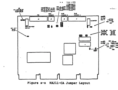
Figure x-x illustrates the factory shipped jumper settings. Table x-x swmnarizes the meaning of each of the jumper settings. The sections
that follow describe the various jumper setting alternatives
available.
KXJll-CA User's Guide
INSTALLATIOH PRELIMINARY 4/3/86.
..
...•
,
..
'''''•• 1 ... II • •
-~
..
'..,..
.."... 1I:!l... ... .., ..
I III • • MKWoe • • lolli' (i1 •• u
Il10..
ta.. ta,
"'G:!]wnI.!J-'
"UI . ' "
tOMIOll c ... , ..
-0
1--_-
---,10
IDOl/In"",
B.
taI
~
I
~
----...
P~Y
.z~.
. I
~
..
-!Hi'
lin ... , . '."C"
~~
-o
D
~bJ!UJ II:D
=-
B .".,-- I ... III . . .I
[image:14.620.94.554.59.411.2]PRELIMINARY 4/3/86 INSTALLATION
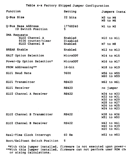
Table x-x Factory Shipped Jumper Configuration Function
Q-BuS Size
Q'-Bus Base Address
10 Switch Position
DMA Requests
SLU2 Channel.A 8036 counter/timer SLU2 Channel B BREAK Enable
HALT Option Selection
Power-Up Option Selection* PROM Addressing*·
SLU1 Baud Rate
SLUl Transmitter SLU1 Receiver
SLU2 Channel A Receiver
SLU2 Channel B Transmitter
SLU2 Channel B Receiver
Real-Time Clock Interrupt Boot/Self test Switch Position
Setting 22 bits
17760240 S Enabled Disabled Enabled Enabled MicrOODT MicroODT 16-bit 9600 RS423 RS423 RS422 RS422 RS422
60 Hz S
Jumpers Installed M3 to M4
M5 to M6 Ml to M2
MIO to MIl M7 to MS Ml2 to Ml3 Ml4 to MlS M16 to M17 MIS to M19 MS6 to M55 M60 to M59 M62 to M61 no jumper M34 to M33 M32 to M31 M30 to M29 M28 to M27 M26 to M25 M24 to M23 M38 to M36 M51 to M50 M42 to M4l M40 to M39 M20 to M2l M52 to M53
*~1ith this jumper installed, firmware is not executed upon power-up.
[image:15.617.54.552.70.690.2]KXJll-CA User's Guide
INSTALLATION PRELIMINARY
2.2.1 Boot/Self test Switch
4/3/86
The boot/selftest switch is a 16 position switch that is used if the board is configured to execute firmware (rather than MicroODT) upon
power-up. It has three functions:
1. It determines what the KXJ11-CA will do when a special interrupt
condition exists (see Section x.x) including whether or not
self tests will run.
2. It determines whether special interrupt handling is performed by
user code or by fi~ware.
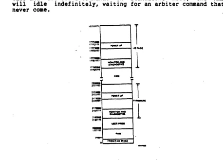
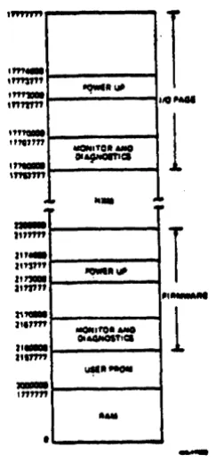
3. It determines where in memory the on-beard 'PROM is mapped. There
are two alternatives low memory or high memory. The memory
maps associated with low and high PROM mapping are sho~n in
Figures x-x, and x-x, respectively.
The location of the boot/selftest switch is shown in pigure x-x. Table x-x summarizes the functions associated with each switch" position.
OCr--
--10
~n
1-o
Switch position
o
1 2 3 4 5 6 7 8 9 10PRELIMINARY 4/3/86
INSTALLATION
Table x-x Boot/Self test Switch Functions
KXJll-CA
Special Interrupt Response
Special Interrupt Handling
User PROM appl~cation code is Firmware
executed. No self tests are performed.
User PROM application code is Firmware
executed. All self tests are performed.
User PROM applfcation code is Firmware
executed. All self tests are performed. The user (P)ROM
checksum test is also performed.
Application cGde is booted from Firmware
a TUS8 via SLUt. All self tests are performed, then the TUS8 primary bootstrap is executed.
MicroODT is entered. No self tests Firmware are performed
All self tests are performed. Firmware
The KXJ!l-CA awaits command from the arbiter via TPRO.
No self tests are performed. Firmware
The KXJ!l-CA aw'aits a boot command from the arbiter via TPRO.
All self tests a~e performed None
continuously. No application code is booted or executed.
Loopback connec~ors (see
Section
x.x.x)
are installedfor these tests. ,_
User PROM application code is User Code
executed. No self tests are performed.
User PROM appli~ation code is User Code
executed. All self tests are performed.
User PROM application code is User Code
executed. All sel~tests are
performed. The user '(P)ROM
checksum test is also performed.
[image:17.612.90.560.87.762.2]KXJll-CA User's Guide
INSTALLATION PRELIMINARY 4/3/86
11
12
13 .
14
15
Notes:
Application code is booted from User Code
a TOSS via SLU1. All self tests are perfo~ed, then the TU58
primary bootstrap is executed.
MicroODT is entered. No self tests User Code are performed
All self tests are performed. User Code
The KXJ11-CA awaits a command from the arbiter via TPRO.
No self tests are performed. User Code
The KXJ11-CA awaits a command from the arbiter via TPRO.
All self tests are performed None
continuously. No application code is booted or executed. Loopback connectors (see
Section x.x.x) are installed
for these tests.
High
High
High
High
High
1. Switch position 5 is the factory shipped configuration.
2. The encoded value of the boot/self test switch position is
available in the KXJCSRB register, bits <7:4>. For example switch position 1 would be encoded as 0001 in KXJCSRB <7:4>.
3. The user· (P)ROM checksum· test looks for a checksum at the highest
word address of user (P)ROM. Similarly, the firmware checksum
test looks for a checksum at the highest word address of the
firmware PROM. Either checksum is calculated and checked
according to the DECPROM algorithm which is as follows:
CHECKSUM =- 0
FOR I =- number of PROM addresses to be checksumed DO CHECKSUM • CHECKSUM + contents of address
(high order carry from addition is discarded) CHECKSUM • ROTATE LEFT ONE BIT
(bitO -> bitl, bitl ->-bit~, •••• ,n-l -> bitO
NEXT I
4. Special interrupt handling can be performed by user code in switch
positions 8-15. This function is useful in applications that need
to continue running after the Q-Bus signals BHALT or BINIT has
been asserted. For switch positions 0 through 7, special
PRELIMINARY 4/3/86
INSTALLATION
5. If the KXJ11-CA is in standalone mode, switch positions 5, 6, 13,
and 14 should not be used. These post ions cause the KXJll-CA to
idle and wait for a command. In standalone mode, the KXJll-CA
will idle indefinitely, waiting for an arbiter command that will never come.
,""'"
''''-'''''"'
" " , . .
,"""'
,.,.",...
''''''''
" "-17'"",
~;
",..
".'''''
"-,
.
.""
•
IIQWtttl/ll
I
=::,.."
....
'''1''
,.,...1/11
1
Itt . . .MOM~MO
01""""
1
\.1111,..
....
....,.UII.IoCI
[image:19.618.72.531.118.447.2]KXJll-CA User's Guide
INSTALLATION PRELIMINARY 4/3/86
, " " " ,
" "
-"",,"
,~
,""'"
• It
..
.
-I"""
J"_
,,"'"
a'"..
1'717' 'I
-
I"""•
~II""
"""'OllMIO
OIAfHOIT1C1
...
....
""
lIIIOI,fQIIMIO OIA4N01'flCl
~.NOII
...
I
I 10 ...
1
•• ~
.
I
,
...
1
-Figure
x-x
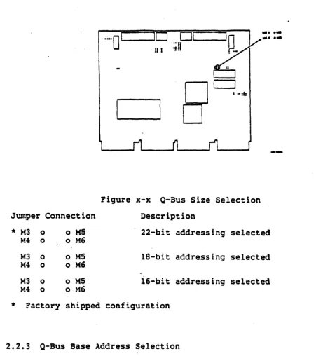
Memory Mapping - PROM in High Memory2.2.2 Q-Bus Size
[image:20.617.252.374.101.366.2]Jumper Connection
*
M3 0 o M5M4 0 o M6
M3 0 o M5
M4 0 o M6
M3 0 o M5
M4 0 o M6
*
Factory shipped0_1 ___
iill
PRELIMINARY 4/3/86
INSTALLATION
, .. tb
...
••••
.•
-Figure
x-x
Q-Bus Size Selection Description22-bit addressing selected
l8-bit addressing selected
i6-bit addressing selected
configuration
2.2.3 Q-Bus Base Address Selection
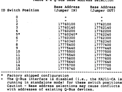
In systems with multiple I/O processor boards, it is necessary to distinguish one from another by making sure that each one has a unique Q-bus base address. This is accomplished on the KXJll-CA by setting the 10 switch and installing or removing a jumper which connects Ml and M2.
Table x-x list~the base addresses that can be selected. Table x-x
lists 22-bit addresses. If the KXJll-CA is configured for 16- or
[image:21.617.58.520.99.607.2]KXJll-CA User's Guide
INSTALLATION PRELIMINARY 4/3/86
specified in Table x-x.
Figure x-x shows the locations of Ml, M2, and the ID switch. The
factory shipped base address is 17760240 •
o Ml
9 M2
.
~
-0
110
01
¢Jj(-::-II I
in
-
....
-0
...
0
--Figure x-x Q-Bus Base Address Selection
PRELIMINARY 4/3/86 INSTALLATION
Table x-x Q-Bus Base Address Selection
Base Address Base Address
ID Switch Position (Jumper IN) (Jumper OUT)
0 + +
1 + +
2 17760100 11762100
3 17760140 17762140
4 17760200 11762200
5* 17760240* 17762240
6 17760300 17762300
7 17760340 17762340
8 17775400 17777400
9 17775440 17777440
10 17775500 17777500
11 17775540 17777540
12 17775600 17777600
13 17775640 17777640
14 17775700 17777700
15 17775740 17777740
*
Factory shipped configuration+ The Q-Bus interface is disabled (i.e., the KXJ11-CA is running in standalone mode) for these switch positions Caution - Base address selections may cause conflicts with addresses of existing Q-Bus devices •.
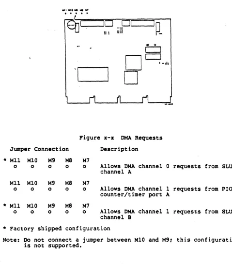
2.2 .. 4 DMA Requests
DMA requests to the on-board DMA transfer controller (DTC) may come front several sources. The KXJ11-CA has a set of jumpers which enable or disable DMA requests from: (1) SLU2 channel A, (2) SLU2 channel B, or (3) the on-board 8036 PIO counter/timer. The location of these
[image:23.612.71.477.93.401.2]KXJll-CA User's Guide
INSTALLATION PRELIMINARY
...
'..."....
""
• • • • •
~I
10
u !
4/3/86
01
10
.. 'I
Ul l
-UI II
I
I
D
• .. d,'I
D
Figure x-x DNA Requests
Jumper Connection Description
*
Mll M10 M9 M8 M70 0 0 0 0 Allows DMA channel
o
requests from SLU2channel A
Mll MlO Kg M8 M7
0 0 0 0 0 Allows DMA channel 1 requests from PIO
counter/timer port A
*
Mll M10 M9 M8 M70 0 0 0 0 Allows DMA channel 1 requests from SLU2
channel B
*
Factory shipped configurationNote: Do not connect a jumper between M10 and K9: this configuration is not supported.
2.2.5 BREAK Enable
[image:24.620.72.552.107.654.2]PRELIMINARY 4/3/86
INSTALLATION
rece'"ived, the J-11 executes MicroODT. The location of this jumper is
shown in Figure
x-x.
BREAK requests are enabled as part of thefactory shipped configuration.
... 0''-___
10
II I
.. ,: "',J
..
~
Figure
x-x
01,-
~'D
iin
! ...IU n
I
a -ais
BREAK Enable
Junlpe r Connect ion Description
*
~t13 0 o M12 Console BREAK requests1-113 0 o M12 Console BREAK requests
*
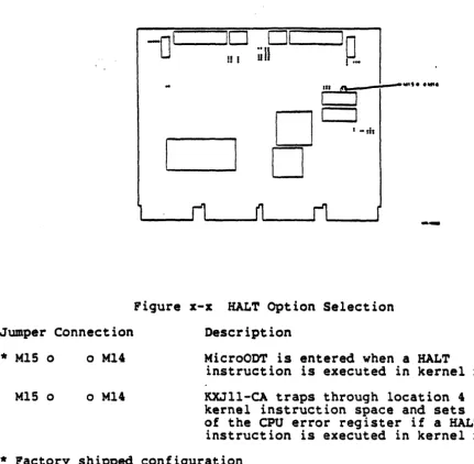
Factory shipped configuration2.2.6 HALT Option Selection
enabled disabled
A jumper on the KXJll-CA dete~ines what action will be taken if a HALT instruction is executed in kernel mode. The location of this jumper is shown in Figure x-x. The jumper affects the state of bit 3
of the Maintenance Register (see Section
x.x).
If the jumper isinstalled (the factory shipped configuration), MicroODT is
unconditionally entered upon the execution of a HALT instruction in
kernel mode. If the jumper is not installed, the KXJll-CA traps
KXJll-CA User's Guide INSTALLATION
Jumper Connection
*
M1S 0 o M14M1S 0 o M14
PRELIMINARY 4/3/86
-0
110 01
'0
!! I
uU
1.-II. f'
_
....,
...
I
0
I
I "fit0
---Figure x-x HALT Option Selection Description
MicroOOT is entered when a HALT
instruction is executed in kernel mode. KXJll-CA traps through location 4 in kernel instruction space and sets bit 3 of the CPU error register if a HALT
instruction is executed in kernel mode.
*
Factory shipped configuration2.2.7 Power-Up Option Selection
The power-up jumper (see Figure x-x) determines what action the
[image:26.620.81.512.115.537.2]-.0
110 01
'0
If I
iill
I .... I
nI
0-I
I
0
I
I ..I
tlt0
PRELIMINARY 4/3/86
INSTALLATION
__ II1II" ... ' •
--Figure
x-x
Power-Up Option SelectionJwnper Connection Description
*
M17 0M17 0
o M16
o M16
MicroODT is entered upon power-up.
The KXJ11-CA bootstraps via location 173000 upon power-up.
*
Factory shipped configuration2.2418 PROM Addressing
The KXJ11-CA can be jumpered to accommodate various PROM types. The
location of the PROM addressing jumper is shown in Figure
x-x.
If thejumper is not installed, the on-board PROMs use 1S-bit addresses.
PROMS such as the Intel ~764 (8K x 8) and 27128 (16K x 8) use 1S-bit
addresses. If the jumper is installed, the PROMs use 16-bit
addx"esses. This accommodates PROMs such as the Intel 27256 (32K x 8)
which use 16-bit addresses. 16-bit PROM addressing is specified as
part of the factory shipped configuration.
KXJ1l-CA User's Guide INSTALLATION
Jumper Connection o Ml9
o MlS
*
o M19o MlS
PRELIMINARY 4/3/86
0
1 -10
lill
i-Figure x-x PROM Addressing Description
--15-bit addressing selected
16-bit addressing selected
*
Factory shipped.configuration2.2.9 SLUl Baud Rate
The jumpers shown in Figure x-x select the default baud rate for the SLU1 transmitter and receiver. The default baud rate for SLUl is set when the KXJll-CA is powered up or reinitialized. It can be changed under software control if KXJCSRJ<3> is
set.
Tablex-x
shows the various baud rates that can be selected. A default baud rate of 9600M60 0 0
M58 0 0
M56 0 0
Baud Rate 38400 19200
*
9600 4800 2400 1200 600 300PRELIMINARY 4/3/86
INSTALLATION
...
...
...
,
,
I
0,--1 ---,I
0
iiU
!-o
D
en "
I
• ".h
Figure x-x SLUl Baud Rate
M59 Factory shipped configuration
-M57 9600 baud
M55
Table x-x SLUl Baud Rate Jumpering M56 to M55 M58 to M57 M60 to M59
In In In
In In Out
In Out In
In Out Out
Out In In
Out In Out
Out Out In
Out OUt Out
2.2.10 SLUl Transmitter
The SLUl transmitter can be jumpered to send either single-ended (RS423) or differential (RS422) asynchronous serial data via connector
J3. The location of the jumpers is shown in Figure x-x. RS423
KXJll-CA User's Guide
INSTALLATION PRELIMINARY 4/3/86
transmission is selected as part of the factory shipped configuration.
-0
110 01
IQyf_ ...
ull
.. . .
!f I i .
n.
'1I
0
I
I ... hI
0
--Figure x-x SLUl Trans.itter
Jumper Connection Description
*
M63 M62 M610 ~o
01
ItS423 transmission selectedM63 M62 M61
[0
oJ 0 RS422 transmission .elected*
Factory shipped confi9uration~2.2.11 SLUl Receiver
The SLUl receiver can be ·jumpered to receive either single-ended (RS423) or differential (RS422) asynchronous serial data via connector
J3. The location of the jumper is shown in Figure
x-xc
RS423Jumper Connection M48 M47
[ 0 oj
* 1'148 1'147
0 0
...
,
••PRELIMINARY 4/3/86
INSTALLATION
-0
Ir...-_ _
IO~ Ol~
---10
II I
un
i ...o
o
III IS
I
riCJure x-x SLUl Receiver Description
RS422 reception selected
RS423 reception selected
*
Factory shipped configuration2.2.12 SLU2 Channel A Receiver
The SLU2 channel A receiver can be jumpered to receive either
single-ended (RS423) or differential (RS422) serial data via connector
Jl. The location of the jumpers is shown in Figure x-x. RS422
KXJll-CA User's Guide
INSTALLATION PRELIMINARY 4/3/86
-0' '---
----,10
If I
. . . MU IIIn • • IIIGt IIUO • •
wa,
...
,
flGl • • filii'
;pr-"-D
D
.11 II
I
I .. ,b
Figure x-x SLU2 Channel A .eceiver
Jumper Connection Description
• H34 K32 1130 K28 K26 K24
0 0
0
0 0 0
M34 0
JIll2 0
1'130 0
M28 0
JIl26 0
M24 0
0] 01
0
0 0 0
M33 JIl31 M29 1'127 M2S M23
o M33
o JIl31
o 1'129
a 1'127
o JIl25
o JIl23
RS422 reception selected
RS423 reception selected
• Factory shipped confi9u~ation
2.2.13 SLU2 Channel B Transmitter
The SLU2 channel B transmitter can be jumpered to send single-ended (RS423), differential (RS422), or party line (CCITT R1360) serial data via connector J2. The location of the jumpers is shown in Figure x-x.
configuration.
KXJll-CA User's Guide INSTALLATION
PRELIMINARY 4/3/86
-0
1JO
01
'0
II I
iill
1-,
..
III
....
•I
D
...
.."...
• •
...
• • •,
...
•
••
0
-Oil
r19ur~ x-x SLU2 Channel I Transmitter
Jumper Connections Description
1'138
M46 M45 M37
(j
K3S•
0 0 0 0 RS422 transmi.sion selectedl136
~ M~
a1 K49
1'138
0
l146 1'145 l137 M3S
0 0
[0
Mfl
a IS423 transmission selected0 0 0
1'151 MSO M49
1'138
0
1'146
K~j
1'137 l13SI
0
0 (2 oI
Party line transmission seiectedM36
0 0 0
*
Factory shipped configuration2.2.14 SLU2 Channel B Receiver
4/3/86 INSTALLATION
ThE! SLU2 channel B receiver can be jumpered to receive single-ended (RS423), differential (RS422), or party line (CCITT Rl360) serial data via connector J2. There are two groups of jumpers involved, as shown
KXJll-CA User's Guide
INSTALLATION PRELIMINARY 4/3/86
...
,
...
... , ... , "lid'
-Ol-··-W-OI __
·\~
-J:;-;-~I
-~
In n
I
, ·,11
Figure x-x SLU2 Channel B Receiver
Jumper Connections Description
1'144 0 0 1'143
J]M20
RS422 reception selected*
M428
1'141 o M21M40 0 0 M39 o 1'122
M43
I]M20
RS423 reception .electedM44 0 0
M42 a 0 1'141 o 1421
1440 0 0 1439 o 1422
01 o M20 party line reception selected
1444(0 1'143
1'142 0 0 M41
I]M21
1'140 0 0 1'139 o M21
*
Factory shipped configuration2e2.15 Real-Time Clock Interrupt
PRELIMINARY 4/3/86 INSTALLATION
Figure x-x. A real-time clock rate of 60 Hz is specified as part of the factory shipped configu,ration •
':Jumper
••
0ill
rn
0...
.
~:-Ol'-~
01,---
---,I
0
iill
1-Figure
x-x
Connection M54
M53 M52 M54 M53 M52
III II
o
D
I
aeal-Time Clock
De.cript~on
60 Hz real-time
I Mlh
Interrupt
clock .elected
50 Hz real-time clock selected
*
ractory shipped configuration--~..,...~---.-...
-2.3 POWER SUPPLY' CONSIDERATIONS
When installing the KXJll~CA, the user must make sure the power supply can handle the extra load presented by the board. The KXJll-CA draws a maximum of 4A at +5V and 2A at +12V. The board adds 2.7 AC loads and 1.0 DC loads to the bus.
In standalone mode, at least four power fingers (backplane
KXJll-CA User's Guide
INSTALLATION PRELIMINARY 4/3/86
fingers for +12VOC must be connected to the power supply.
2.4 INSTALLING THE KXJll-CA INTO A BACKPLANE
The KXJll-CA plugs into any DEC standard quad height backplane (see
Pigure x-x). No special backplane wiring or jumpering is required to
accommodate the KXJll-CA. Keep in mind that the grant structure must
be preserved if there are blank slots between the ~ll-CA and the top
of the backplane. This can be accomplished by inserting grant cards
where appropriate. Figure x-x shows an example of the use of grant
cards. The dual height grant card (M8659) pres.rves grant continuity for slots A and B and grant card G7272 preserves the DNA and interrupt
grant continuity for slot C. Also keep in mind that the KXJll-CA
board must be configured for the proper Q-Bus adqress size.
Figure x-x Backplane Installation
,
4/3/86 INSTALLATION
lC;omponent Side Solder Side
KXJll-CA KXJll-CA
:~in Signal Pin Signal
-~----
----~-CAl NC CA2 +5V
CBl NC CB2 NC
CCl NC ce2 GND
(:01 NC CO2 NC
C:El NC CE2 NC
Cptl NC CF2 NC
CHl NC CH2 NC.
CJl NC CJ2 NC
C:Xl NC CK2 Nt
C:Ll NC CL2 NC
Ofl NC 012 IAR. L (Note 2)
CNl NC CN2 IAR L (Note 2)
CPl NC CP2 NC
CRl NC CR2 OMG L (Note 3)
CSl NC eS2 OMG L (Note 3)
CTl GND CT2 NC
(:Ul NC CU2 NC
CVl NC CV2 NC
DAl NC OA2 +5V
DBl NC DB2 NC
DCl NC De2 GND
001 NC 002 NC
DEl NC DE2 NC
D'Fl NC DF2 NC
OHl NC DH2 NC
OJl NC DJ2 NC
OKl NC OK2 NC
DLl NC DL2 NC
O:Ml NC DM2 NC
D.Nl NC DN2 NC
OPl NC DP2 NC
O:Rl NC DR2 NC
DSl NC DS2 NC
D'rl GND DT2 NC
001 NC DU2 NC
DVl NC DV2 NC
Notes:
1. NC
=
Not connected2. Pin CM2 is jumpered to pin CN2 for the interrupt acknowledge daisy chain.
KXJll-CA User's Guide
INSTALLATION PRELIMINARY
4/3/86
2.5 CONNECTORS AND EXTERNAL CABLING
The KXJll-CA communicates with external devices via a parallel I/O connector (J4) and three serial I/O connectors (Jl, J2, and J3). This section specifies the pin assignments of these connectors and ·lists the types of cables that can be used with each.
2.5.1 Parallel I/O Interface (J4)
The parallel I/O (PIO) interface signals appear at connector J4.
These signals are buffered. They can be driven over a 50 ft.
distance via a ribbon cable or round cable with a 40-pin AMP contact housing at each end. A PIO cable is not provided wi th the KXJll·-CA. We recommend the use of the following cables, available from Digital Equipment Corporation:
BC06 R shielded ribbon cable BCOS L "mirror image" cable
Figure
x-x
shows the pin assignments for J4, the parallel I/Oconnector.
INSTALLATION
2.5.2 Serial I/O Lines (Jl, J2, J3) The KXJll-CA has three serial I/O lines:
o SLU2 channel A (Jl), a synchronous/asynchronous serial line with modem control
o SLU2 channel B (J2), a synchronous/asynchronous serial line
without modem ~ontrol
o SLUl (J3), the console asynchronous serial line (no modem control) Each serial line is compatible with the EIA RS232-C and RS422/RS423 protocols. In addition, SLU2 channel B (J2) is compatible with the CCITT R1360 party line protocol. Interfacing the KXJll-CA with 4-20 rnA current loop devices via the serial lines can be done by using the
DLVII-KA option.
The user must supply his own serial line cables. We recommend the following cables (available from Digital Equipment Corporation) for J2 and J3:
BC20N-05
BC21N-05
BC2()M-50
AS-foot EIA RS232-C null modem cable for a direct connectiOA between the KXJ11-CA and an EIA terminal. This cable has a la-pin (2
x
5) AMP female connector on one end and a 25-pin RS232-C female connector on the other.A 5-foot EIA RS232-C modem cable for a connection between the KXJll-CA and a modem or acoustic coupler. This cable has a lO-pin (2 x 5) AMP female connector on one end and a 2S-pin RS232-C male connector on the other.
A 50-foot EIA RS422 or RS423 cable for a direct connection between the KXJll-CA and a remote processor. Used in
applications requiring. high data transmission speeds (up to 19.2 K baud). This cable has a 10-pin (2 x 5) AMP. female connector on each end.
The pin designations for J2 and J3 are shown in Figure
x-x.
KXJll-CA User's Guide
INSTALLATION PRELIMINARY 4/3/86
Figure x-x J2 and J3 Pin A •• ignments (lO-pin)
There is no standard cable available from Digital Equipment
Corporation for SLU2 channel A; the user needs to construct his own. Figure
x-x
illustrates the pin assignments for SLU2 channel A (Jl). Tablesx-x
through x-x show the correspondence between the pins of the standard connectors for the RS422/RS423, RS232, and CCITT protocolsand the pins of Jl. These tables make it easy to construct an
appropriate cable. The KXJll-CA register address associated with each signal is specified in the last column of each table for ease of programmer reference. The register descriptions in Chapter x provide
.. ~
..
.
PRELIMINARY 4/3/86
INSTALLATION
• •
•
•• "' w
KXJll-CA User's Guide PRELIMINARY 4/3/86 INSTALLATION
Table x-x RS422/RS423 Interface to J1
Pin Circuit Direction Function RS-232 CCITT Pin Location
1 SHIELD Protective Ground
2 SI From Modem CI 112 S,E 17777522
3 SPARE
4 SO To Modem Send Data (+) BA 103 23,AA 17775706
6,F
5 ST From Modem Send Timing (+) DB 114 12,N 11777520
6 RD From Modem Receive Data (+) BS 104 8,J 17775702
7 R5. To Modem Request to Send (+) CA 105 13,P 17775704
18,V
8 RT From Modem Receive Timing (+) DD 115 l4,R 17775720
9 CS From Modem Clear to Send (+) CS 106 16,T 17775700
10 LL To MQdem Local Loop 141 25,CC Dummy Gen~
11 DM From Modem Data Mode (+) CC 107 22,Z 17775710
12 TR To Modem Terminal Ready (+) CD 108/2 33,M 17777520
26,DO
-13 RR From Modem Receiver Ready (+) CF 109 24,'B8 17775700
..
"14 RL To Modem Remote Loop 140 9,K Dummy Gene
15 IC From Modem Incoming Call CE 125 20,X 17775710
16 SF/SR To Modem Select Frequency 126 3,C 1777752f
Signal Rate Select CH 111 3,C
17 TT To Modem Terminal Timing (+) DA 113 30,JJ 17777530
lO,L
18 TM From Modem Test Mode 142 5,E 17777522
19 SG To Modem Signal Ground AB 102 40,~
20 RC From Modem Receive Common 102b 2,S
21 SPARE
22 SDR To Modem Send Data (-) 31,KK
23 STR From Modem Send Timing (-) 38,TT
24 RDR From Modem Receive Data (-) 15,5
25 RSR To Modem Request to Send (-) 32,LL
26 RTR From Modem Receive Timing ( -) 37,SS
27 CSR From Modem Clear to Send (-) 35,PP
28 IS To Modem Terminal in Service 3,C 17777520
29 DMR From Modem Data Mode (-) l7,V
30 TRR To Modem Terminal Ready (-) 19,W
31 RRR From Modem Receiver Ready (-) 7,H
32 55 To Modem Select Standby 116 28,FF Dummy Gen.
33 5Q From Modem Signal Quality CG 110
34 N5 To Modem New Signal
35 TTR To Modem Terminal Timing (-) 27,EE
36 SB From Modem Standby Indication 117
No1:es on Figure x-x and Table x-x:
PRELIMINARY 4/3/86
INSTALLATION
1. Pins K 9, 25
ce,
and 28 FF are driven by dummy generators whichdisable RL (CCITT 140), LL (CCITT 141), and SS (CCITT 116)
respectively.
2. The label.·NC indicates no connection.
3. The suffix R in a three-letter pin label (such as RDR) signifies that the pin is associated with the return side of a differential driver or receiver.
4. Circuit IS can be redefined to mean SF. Or IS can be redefined to SR. In the second case, TM is also redefined to SI.
KXJ11-CA User's Guide
INSTALLATION PRELIMINARY 4/3/86
Pin Circuit Direction Function
1 AA Protective Ground
2 BA To Modem Transmitted Data
3 BS From Modem Received Data
4 CA To Modem Request to Send
5 CS From Modem Clear to Send
6 CC From Modem Data Set Ready
7 AS Signal Ground
8 CF From Modem Receiver Ready
9 (From Modem) (+ DC Test Voltage)
10 (To Modem) (- DC Test Voltage)
11 Unassigned
12 SCF From Modem Secondary Carrier
Detector
13 SCB From Modem Secondary Clear to
Send
14 SBA To Modem Secondary Trans- .
mitted Data
15 DB From Modem Transmitter Clock
16 SBB From Modem Secondary Received
Data
17 DO From Modem Receiver Clock
18 To Modem Receiver Dibit Clock
19 SCA To Modem Secondary Request to
Send
20 CD To Modem Data Terminal Ready
21 CG From Modem Signal Quality
Detector
22 CE From Modem Ring Indicator
23 CHICI To Modem Data Rate Selector
24 DA To Modem External Transmitter
Clock
25 CN To Modem Force Busy
CCITT 101 103 104 105 106 107 102 109 122 121 118 114 119 115 120 108/2 110 125 111 112 113
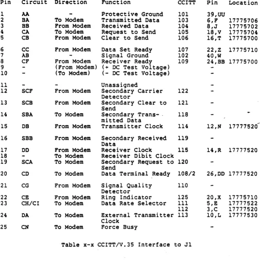
Table x-x CCITT/V.35 Interface to Jl
Pin Location
39,00
6,F 17775706
8,J 17775702
18,V 17775704 16,T 17775700 22,Z 17775710 40,W
24,BB 17775700
... "
12,H 17777520
14,R 17777520
26,DD 17777520
20,X 17775710
5,! 17777522
3,C 17777520
[image:46.613.74.580.112.633.2]Pin A B C 0 E F H J R T V X Y AA P S U W
Circuit Direction Function
101 Protective Ground
102 Signal Ground
105 To Modem Request to Send
106 From" Modem Ready for Sending
107 From Modem Data Set Ready
109 From Modem RCV Line Signal Oet
10S/1 To Modem Con:nect Data Set
10S/2 To Modem Data Terminal Ready
125. From Modem Calling Indicator
104 From Modem Received Data A
104 From Modem Received Data B
115 From Modem Receive Timing A
115 From Modem Receive Timing B
114 From Modem Transmit Timing A
114 From Modem Transmit riming B
103 To Modem Transmit Data A
103 To Modem Transmit Data B
113 To Modem Terminal Timing A
113 To Modem Terminal Timing B
2.5.3 Loopback Connectors
PRELIMINARY 4/3/86
INSTALLATION
RS232 RS449 Pin Location
AA 39,00
AB SG 40,W.
CA RS lS,V 17775704
CB CS 16,T 17775700
CC OM 22,Z 17775710
CF RR 24,8B 17775700
CO TR 26,00 17777520
CE IC 20,x 17775710
BB RD 8,J 17775702
RD
DO RT 14,R 17777520
RT
DB ST 12,N 17777520
ST
BA SO 6,F 1 ~775706
SD
DA TT 10,L 17777530
TT
Loc)pback connectors (not provided) are attached to the ser"ial or parallel communication potts to determine whether or not they are
operating correctly (see Figure
x-x).
They are typically used inconjunction with the running of diagnostic programs and in some
firmware self tests (see Sections
x.x.x
andx.x.x).
These connectors may be ordered from Digital Equipment Corporation or may be built by the user. If the user wants to make his own loopback connectors, see Appendixx.
There are three different types of loopback connectors. A lO-pin
[image:47.613.45.594.89.602.2]KXJ11-CA User's Guide
INSTALLATION PRELIMINARY 4/3/86
l~oooOQeQQol
;;
sa :r =- ... ., Figure x-x Loopback Connectors2.6 ERROR DETECTION AND REPORTING WITH THE LEOS
There are four LEOs on the edge of the KXJ11-CA board which the native
firmware uses to indicate the state of the board. These are
especially useful for diagnostic purposes during power-up or
reinitialization. Using the LEDs, the user can quickly verify that the board is operating properly or, if there is a problem with the
board, can help locate the difficulty. Table x~x summarizes the
conditions the LEOs can indicate.
Upon power-up or reinitialization, all four LEOs are illuminated for approximately 1/2 second if they are working properly'. The LEDs are labeled L~ through Ll from left to right as vi~wed from the back of
the box when the KXJ11-CA is installed 1n a backplane. If the
KXJll-CA runs its self tests (this is determined by the setting of the boot/self test switch), L4 is off and Ll - Ll are on as the self tests run. If one of the self tests fails, L4 is illuminated and L3 Ll indicate the test that failed. ,Self tests are run in the order listed in Table x-x. Thus, if a test fails, the user can also determine which tests (if any) passed.
If all the self tests run without error, the KXJll-CA performs a boot operation. The boot/self test switch setting determines what func~ion
PRELIMINARY 4/3/86 INSTALLATION
that self tests are not run. If that is the case then L4 is off and L3 - Ll indicate the state of the board as it executes code.
Table x-x LED Display Definitions LEDs
L4 L3 L2 Ll Meaning
x x x x All LEDs on for 1/2 sec. at the start of a power-up or reinitialization operation
x x x x Can't access Control/Status Registers in I/O page
x 0 0 0 DMA or RTC test failed
x 0 0 x RAM test failed
x 0 x 0 ROM checksum test failed
x 0 x x Serial line test of SLUl failed
x x 0 0 Serial line test of SLU2 channel A failed
x x 0 x Serial line test of SLU2 channel B failed
x x x 0 Parallel port test failed
0 x x x Auto self tests running
0 x x 0 Loopback tests running
0 x 0 x Q-Bus OOT mode
0 x 0 0 Fatal runtime error
0 0 x x Waiting for command
0 0 x 0 Performing DTC load
0 0 0 x TUSS primary bootstrap executing
0 0 0 0 Executing non-native code
Quick LED Reference LEDs
L4 L3 L2 Ll Meaning
x Self test error detected
x x x x Fatal self test error detected
0 No self test errors detected
0 0 0 0 Application running without error
Note: x : I ON
o : I OFF
: I Don't care <either ON or OFF)
2.7 DIAGNOSTIC TESTING WITH XXDP+
TheKXJll-CA can be tested by running XXDP+, a diagnostic operating
system that is booted from the user's system disk. This section
[image:49.613.62.574.165.642.2]KXJ11-CA User's Guide INSTALLATION
(AC-F348F-MC).
PRELIMINARY 4/3/86
When the user has successfully booted XXDP+ from his system disk, a message
such
as the one shown below appears on the console terminal. The items that are blank (underscore) indicate values that are system dependent.BOOTING UP XXDP-SM SMALL MONITOR XXDP-SM SMALL MONITOR VERSION BOOTED FROM
KW OF MEMORY NON=UNIBUS SYSTEM RESTART ADDR: 152010
THIS IS XXDP- SM TYPE "H" or "H/t" FOR HELP
When the "period" prompt appears, the user types in: R KXJ008<CR>
This initiates the running of the tests. The message KXJ008.BIN then~;
appears on the console followed by several lines of system
information. Then the following should appear: USE <ESC> TO HALT
KXJ FUNCTIONAL TEST
SWR OCTAL FUNCTION
.----,.-,-
..
-...,~----15 100000 HALT ON ERROR
14 040000 INHIBIT ERROR SUMMARY
13 020000 INHIBIT ERROR REPORTS
12 010000 UNUSED
10 002000 UNUSED
09 001000 LOOP ON ERROR
08 000400 LOOP ON TEST IN SWR<6:0>
07 000200 INHIBIT TEST NUMBER/TITLE
SWR :II 140000 NEW :II
At this point, the user should type in 100000<CR> which runs the tests until an error is detected. As the tests run, their results are displayed on the console. If an error is detected, a self-explanatory error message is displayed and the tests halt. To rerun the tests after an error occurs, the user should halt the system and type in:
@152010G<CR>
R KXJ008<CR>
INSTALLATION
To repeat the procedure· described previously. If no errors are