Testing of a Lightweight SiC Power Module for Avionic Applications
E. Gurpinar
∗, S. Lopez-Arevalo
∗, J. Li
∗, D. De
∗, A. Castellazzi
∗, L. Mills
†∗PEMC Group, The University of Nottingham, U.K.,†Semelab Limited, U.K.
Email: [email protected]
Keywords: SiC, silicon carbide, MOSFET, SiC power mod-ule, high-frequency inverter, three-phase inverter, avionic sys-tems
Abstract
Functional and performance tests of a three-phase, two-level power module based on CREE 1.2kV SiC MOSFETs for avionic applications is presented in this paper. SiC devices have superior properties over conventional Si devices at high voltage operations and these properties make SiC devices at-tractive for avionic industry in order to reduce size of power electronic converters while maintaining high efficiency. This paper starts with a brief explanation of thermo-mechanical sign approach of SiC power module. Thermo-mechanical de-sign is followed by test setup and experimental results for dif-ferent load and switching frequency conditions. The module is tested up to 540V DC link voltage, 6kW output power with 100kHz switching frequency. Experimental results show that the module can be successfully operated with high efficiency at high switching frequencies.
1
Introduction
Silicon carbide (SiC) has superior properties over silicon (Si), which has been the dominant semiconductor material for power semiconductor devices, that make SiC a potential can-didate to replace Si for high voltage, high power applications. SiC has three times higher energy gap and seven times higher electric breakdown field that allow SiC to have higher voltage withstand capability. In addition to high voltage withstand capability, SiC has three times higher electron velocity than Si, that leads to operate SiC at high switching frequencies [1–5]. High voltage and high switching capability of SiC resulted in commercially available active and passive power devices like MOSFET, normally on and off JFETs, BJT and Schottky diode at 1200V from different manufacturers. It should be noted that due to high on-state resistance at high voltage applications (>1000V), Si MOSFET is considered impractical [6].
SiC devices has already drawn attention from avionic indus-try due to its high performance at high frequency, high power and high temperature applications [7]. In [8], switching per-formance and robustness of two 1200V SiC MOSFETs from different manufacturers are compared. Gate oxide reliability of SiC MOSFETs for more-electric-aircraft applications is dis-cussed in [4]. Switching performance evaluation of Si and
(a)
[image:1.595.310.544.208.528.2](b)
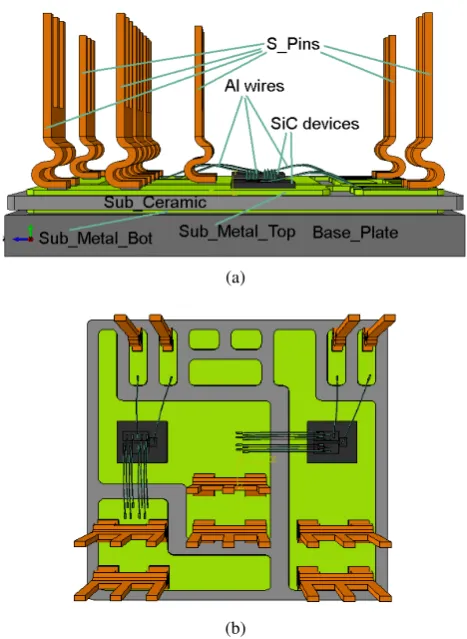
Figure 1: Half-bridge switch: (a) side view and (b) top view
SiC for avionic applications in [9] shows that SiC devices have ten times less switching losses in comparison to Si devices for given operating conditions.
show that SiC switches demonstrate high degree of stability in leakage current, on-state resistance, junction temperature and switching energy variation. In [11], a direct liquid cooled SiC power module is presented where direct liquid cooling provides better cooling performance of the module and enables exploitation of the SiC performance. Experimental results in this paper show that by using direct cooling and SiC devices, current density of the module can be increased at least three times and power losses can be reduced 50%, in comparison to all-Si modules.
In this paper, a three-phase, two-level SiC power module based on CREE CPMF-1200-S080B Z-FETTMis presented. In sec-tion 2, thermo-mechanical design of half-bridge and power module is presented . Experimental setup, components and test strategy are presented in section 3. Section 3 is followed by the experimental results of the module with different load, fre-quency and power conditions in section 4.
2
Design of Half-Bridge Switch and Power
Module
The overall design of the power module is based on integration of three individual half-bridge legs in a single package. Dimensions of each MOSFET die is4.08×4.08×0.365mm and the pin arrangement of each device has been designed to maximise the switching performance. Half-bridge design of the module is given in Figure 1.
SiC MOSFETs and all the pins are soldered onto the top metal substrate (Sub Metal Top), and the bottom metal substrate
(Sub Metal Bot) is soldered on the base plate (Base Plate). Thermo-mechanical analysis and simulation is mainly to in-vestigate the effects of type and thickness of the substrate and base plate on the thermal and thermo-mechanical performance of the switch module. Therefore, all the solder joints are made of with eutectic Sn-3.5Ag solder and fixed to a constant thickness of 100µm and the Al wire-bonds are fixed to a constant diameter of 125µm. Because the application does not target specifically high temperature applications, aluminium wire-bonds are used for interconnections to the device top-side.
For substrate, two types of substrates commonly used in power modules have been considered. The first one is0.4mm and
0.3mm thick active brazed Cu on both sides of 1mm or
0.635mm thick AlN tile. The second one is0.4mm and0.3mm thick (or0.3mm and0.2mm) active brazed Cu on both sides of 0.3mm or0.635mm thick Si3N4 tile. During the
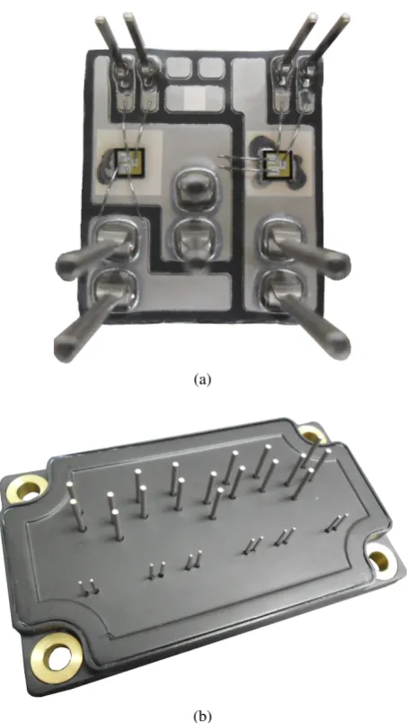
thermo-mechanical analysis, AlSiC-9 and AlSiC-12 composite base plates have been considered. According to thermo-mechanical results, 2mm thick AlSiC-9 base plate and AlN based substrate with 0.635mm AlN tile are selected for optimum design with respect to the provided loss mission profile of SiC switches. Assembled half bridge and power module are given in Figure 2a and 2b respectively.
3
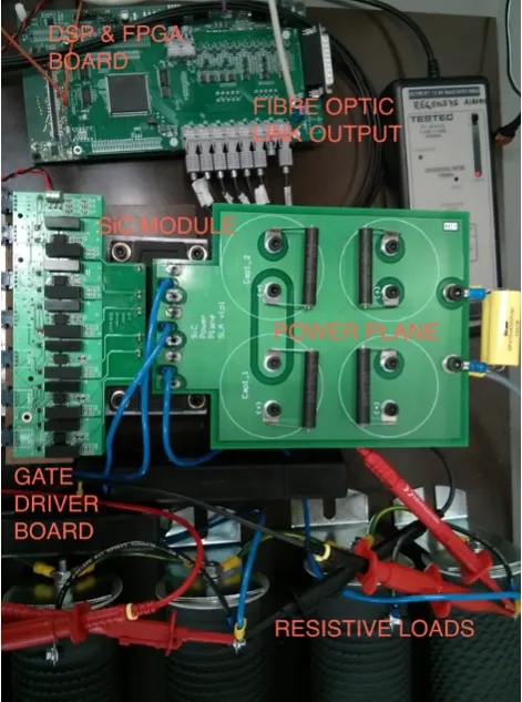
Test Setup
A flexible test setup has been designed in order to test five different modules that have been manufactured and the schematic and photo of the test setup are given in Figure 3 and 4 respectively. The power plane in the setup is connected to four electrolytic capacitors(350V, 3.3mF each)with discharge and balancing resistors (47kΩeach), and the power plane is mounted on the SiC module power pins.
(a)
[image:2.595.315.542.210.612.2](b)
Figure 2: Lightweight SiC MOSFET module: (a) half bridge and (b) assembled module
In-S1
S2
S3
S4
S5
S6
S 1S 2
S 3
S 4
S 5
S 6
EA PS 81500-30 3U
DC Power Supply
DC +DC
-DSP+FPGA
Board
E nable S 1 S 2 S 3 S 4 S 5 S 6
Gate Driver
Board
S 1 S 2 S 3 S 4 S 5 S 6 E nable
S 1* S 2* S 3* S 4* S 5*
S 6* +5V 0V
S 1 S 2 S 3
S 4 S 5
S 6
DC Power Supply
+5V0VA
B
C
Resistive Load, 15ohm 1000W each
DC link 3.3mF, 47k ohm each
DC+
SiC MOSFET Module
[image:3.595.66.530.94.358.2]DC-Fibre Optic
Link
Figure 3: Test setup
put DC link voltage is 540V fixed input that represents DC bus in an avionic system and the converter test at full load(6kW)
and half load(3kW)conditions. Output phase-to-neutral RMS voltage is set to 115V with 50Hz fundamental frequency.
4
Experimental Results
Testing of converter started with half load at 5kHz switch-ing frequency and continued with 20, 40, 60, 80 and 100kHz switching frequencies respectively. For each switching fre-quency condition, the DC power supply voltage and current, and the load voltages and currents are measured in order to ob-serve overall performance of the system. Additional to this, the gate-source voltageVGS and drain-source voltageVDS
wave-forms of switchS1 are recorded to assess the performance of
SiC MOSFET under different load and switching frequency conditions.
4.1 MOSFET Switching Performance
Turn-on and turn-off switching performance of MOSFET S1 in the module is assessed at different switching frequency conditions and turn-on and turn-off switching results are presented with gate-source voltage VGS and drain-source
voltageVDSwaveforms in Figure 6a and 6b respectively.
Experimental results show that turn-on time of S1 is less than 60ns under all different switching frequency conditions. Turn-on time increases from 35ns to 55ns as the switching frequency is increased from 5kHz to 100kHz. Under all switching frequency conditions, turn-on duration stays within
[image:3.595.310.546.405.722.2]expected range and is significantly shorter than turn-on time of a conventional 1200V Si IGBT at given load conditions. Turn-off time of SiC MOSFET is also under 60ns under all switching frequency conditions. In parallel to turn-on performance, turn-off time increases from 30ns to 60ns as the switching frequency is increased from 5kHz to 100kHz.
According to device datasheet in [13], forward voltage drop of body diode is 3.5V that is twice as forward voltage drop of a discrete 1200V SiC Schottky diode in [14]. Dead-time be-tween top and bottom switch in each phase leg is set to 500ns during the experiments and the body diode of the complemen-tary switch in the phase leg is in conduction during dead-time. The results show that dead-time value can be set to smaller val-ues in order to decrease the conduction time of body diode of MOSFET that will lead to increase in system efficiency.
4.2 Output Current
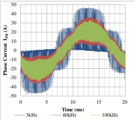
The converter is tested at different switching frequencies with resistive and inductive load conditions. Current waveforms of phase A at full resistive load condition with 5, 60 and 100kHz switching frequencies are presented in Figure 5. The results show that phase current is discontinuous at 5kHz and as the switching frequency increases, phase current becomes contin-uous due to leakage inductance at the resistive loads and phase cables. Measured leakage inductance at each phase is approxi-mately 90µH. -50 -40 -30 -20 -10 0 10 20 30 40 50
0 5 10 15 20
P h a se C u r re n t
IPH
(A
)
Time (ms)
[image:4.595.310.545.86.737.2]5kHz 60kHz 100kHz
Figure 5: Output phase A current waveforms for different switching frequencies at full load.
Output current waveforms for resistive load at 100kHz switch-ing frequency and for inductive load at 5kHz and 100kHz switching frequencies are presented in Figure 7a and 7b respectively. Inductive load provides continuous phase current at low switching frequencies. In Figure 7b, current ripple at 100kHz is much smaller than the ripple at 5kHz but high current spikes occur during deadtime events and these events
-100 0 100 200 300 400 500 600 700 -10 -5 0 5 10 15 20 25 30
0 100 200 300 400
D ra in -s o u r c e v o lt a g e VD S (V ) G a te -s o u r ce v o lt a g e VG S (V ) Time (ns)
5kHz Vgs 60kHz Vgs 100kHz Vgs
5kHz Vds 60kHz Vds 100kHz Vds
(a) -100 0 100 200 300 400 500 600 700 800 -15 -10 -5 0 5 10 15 20 25 30
0 100 200 300 400 500
D r a in -s o u r c e v o lt a g e VD S (V ) G a te -s o u r c e v o lt a g e VG S (V ) Time (ns)
5kHz Vgs 60kHz Vgs 100kHz Vgs
5kHz Vds 60kHz Vds 100kHz Vds
(b)
[image:4.595.51.285.429.637.2]-40 -30 -20 -10 0 10 20 30 40
0 5 10 15 20
P
h
a
se
C
u
rr
en
t
IPH
(A
)
Time (ms)
Phase A Phase B Phase C
(a)
-35 -25 -15 -5 5 15 25 35
0 5 10 15 20
P
h
a
se
C
u
rr
en
t
IPH
(A
)
Time (ms)
A 100kHz B 100kHz C 100kHz
A 5kHz B 5kHz C 5kHz
[image:5.595.51.287.84.536.2](b)
Figure 7: Output current waveforms for different switching fre-quencies with : (a) resistive load and (b) inductive load
introduce noise to output current waveform. Both Figure 7a and 7b proves that the power module can successfully operate with 6kW resistive and inductive load conditions between 5kHz and 100kHz switching frequencies.
Efficiency of the converter is measured at 6kW output power for different switching frequencies. Efficiency curve is pre-sented in Figure 8. The efficiency curve shows that SiC mod-ule maintains high efficiency between 5kHz and 100kHz. This high performance of the module at high switching frequencies is beneficial for achieving high power density by reducing size of passive components.
95 95.5 96 96.5 97 97.5 98
0 10 20 30 40 50 60 70 80 90 100
E
ff
ic
ie
n
c
y
(%
)
Switching Frequency (kHz)
Figure 8: Efficiency of the converter at 6kW output power for different switching frequencies
5
Conclusion
In this paper, thermo-mechanical design, test setup, test ap-proach and experimental results of a three-phase two-level SiC power module are presented. Thermo-mechanical design is based on minimising weight of the module while maintaining maximum reliability for avionic applications. A flexible test setup is designed in order to test the module in a power con-verter under different load and switching frequency conditions. Experimental results show that SiC power module can success-fully operate under resistive and inductive loads up to 6kW out-put power between 5kHz and 100kHz switching frequencies. The converter maintains high efficiency at high switching fre-quencies due to superior switching and conduction properties of SiC devices. The module can be used to design high fre-quency, high power density converters with high efficiency in avionic systems.
Acknowledgements
Authors would like to thank European Union Clean Sky JTI programme for funding of Robust Silicon Carbide Technology for Aerospace DC-DC Conversion(RoSiC)project.
References
[1] B. Baliga, “Trends in power semiconductor devices,”
IEEE Transactions on Electron Devices, vol. 43, no. 10,
pp. 1717–1731, 1996.
[2] C. Weitzel, J. Palmour, C. Carter, K. Moore, K. Nordquist, S. Allen, C. Thero, and M. Bhatnagar, “Silicon carbide high-power devices,”IEEE Transactions
on Electron Devices, vol. 43, no. 10, pp. 1732–1741,
1996.
[3] J. Millan, P. Godignon, X. Perpinya, A. Perez-Tomas, and J. Rebollo, “A Survey of Wide Band Gap Power Semicon-ductor Devices,”IEEE Transactions on Power Electron-ics, no. c, pp. 1–1, 2013.
[image:5.595.307.548.86.229.2]MOSFET for high temperature aeronautic applications,”
in 2013 IEEE ECCE Asia Downunder, pp. 385–391,
IEEE, June 2013.
[5] A. Castellazzi, T. Funaki, T. Kimoto, and T. Hikihara, “Thermal instability effects in SiC Power MOSFETs,”
Microelectronics Reliability, vol. 52, pp. 2414–2419,
Sept. 2012.
[6] S. Safari, A. Castellazzi, and P. Wheeler, “Experimental and Analytical Performance Evaluation of SiC Power De-vices in Matrix Converter,”IEEE Transactions on Power
Electronics, no. c, pp. 1–1, 2013.
[7] Z. Chen, Y. Yao, D. Boroyevich, K. Ngo, P. Mattavelli, and K. Rajashekara, “A 1200 V, 60 A SiC MOSFET Multi-Chip Phase-Leg Module for High-Temperature, High-Frequency Applications,” IEEE Transactions on
Power Electronics, no. c, pp. 1–1, 2013.
[8] S. Lefebvre, M. Berkani, Z. Khatir, A. Ibrahim, and A. Bouzourene, “Investigation of 1.2 kV investigation of SiC MOSFETs for aeronautics applications,” in2013 15th European Conference on Power Electronics and
Ap-plications (EPE), pp. 1–9, IEEE, Sept. 2013.
[9] B. Cougo, H. Schneider, and T. Meynard, “Accurate switching energy estimation of wide bandgap devices used in converters for aircraft applications,” in2013 15th European Conference on Power Electronics and
Applica-tions (EPE), pp. 1–10, IEEE, Sept. 2013.
[10] R. A. Wood and T. E. Salem, “Evaluation of a 1200-V, 800-A All-SiC Dual Module,” IEEE Transactions on
Power Electronics, vol. 26, pp. 2504–2511, Sept. 2011.
[11] Z. Liang, P. Ning, and F. Wang, “Development of Ad-vanced All-SiC Power Modules,”IEEE Transactions on
Power Electronics, vol. 29, no. 5, pp. 1–1, 2013.
[12] R. A. Wood and T. E. Salem, “Long-term operation and reliability study of a 1200-V, 880-A all-SiC dual module,”
International Symposium on Power Electronics Power
Electronics, Electrical Drives, Automation and Motion,
pp. 1520–1525, June 2012.
[13] CREE Inc, “CPMF-1200-S080B SiC MOSFET,”
Datasheet, 2013.