3D ToF-SIMS Imaging of Polymer Multilayer Films Using Argon
Cluster Sputter Depth Pro
fi
ling
James Bailey,
§Rasmus Havelund,
‡Alexander G. Shard,
‡Ian S. Gilmore,
‡Morgan R. Alexander,
†James S. Sharp,
§and David J. Scurr
*
,††Laboratory of Biophysics and Surface Analysis, University of Nottingham, Nottingham NG7 2RD, England ‡National Physical Laboratory, Teddington, Middlesex TW11 0LW, England
§School of Physics & Astronomy and Nottingham Nanoscience and Nanotechnology Centre, University of Nottingham, Nottingham
NG7 2RD, England
*
S Supporting InformationABSTRACT: ToF-SIMS imaging with argon cluster sputter depth profiling has provided detailed insight into the three-dimensional (3D) chemical composition of a series of polymer multilayer structures. Depths of more than 15μm were profiled in these samples while maintaining uniform sputter rates. The 3D chemical images provide information regarding the structure of the multilayer systems that could be used to inform future systems manufacturing and development. This also includes measuring the layer homogeneity, thickness, and interface widths. The systems
analyzed were spin-cast multilayers comprising alternating polystyrene (PS) and polyvinylpyrrolidone (PVP) layers. These included samples where the PVP and PS layer thickness values were kept constant throughout and samples where the layer thickness was varied as a function of depth in the multilayer. The depth profile data obtained was observed to be superior to that obtained for the same materials using alternative ion sources such as C60n+. The data closely reflected the“as manufactured”
sample specification, exhibiting good agreement with ellipsometry measurements of layer thickness, while also maintaining secondary ion intensities throughout the profiling regime. The unprecedented quality of the data allowed a detailed analysis of the chemical structure of these systems, revealing some minor imperfections within the polymer layers and demonstrating the enhanced capabilities of the argon cluster depth profiling technique.
KEYWORDS: ToF-SIMS, argon, depth, profiling, polymer, multilayers
■
INTRODUCTIONThinfilm polymer structures play a key role in a variety of areas including opticalfilters and reflectors,1,2polymer electronics,3,4 optoelectrical devices5,6 and drug delivery.7,8 There has been growing interest in preparing these types of devices using polymer nanostructures. This is due to their ease of manufacture and reduction in cost when compared to inorganic alternatives.3,9,10 However, these types of devices will not be commercially viable until their performance characteristics become comparable to those made from inorganic materials. This has led to various investigations into how the efficiency of these devices depends upon the design, structure, chemical composition and/or preparation technique. The structure of these polymer devices is frequently investigated using techniques such as scanning electron microscopy (SEM), transmission electron microscopy (TEM), X-ray scattering and neutron reflectivity.11,12 There is only a small measurable contrast between different polymers when using SEM and TEM. This can be increased by preferentially staining one or more polymers in the sample.2However, using a chemical stain can damage the sample and its structure. Similarly, it is also difficult to measure the contrast between different polymers when using X-rays. High intensity X-ray beams must be used when measuring polymer structures which can damage the
samples during measurements, making it difficult to obtain reproducible and reliable results.11,12 Neutron reflectivity methods are capable of accurately measuring the structure of polymer samples. However, large and expensive facilities are required and the samples often need to be prepared using deuterated polymers in order to increase the scattering contrast.11,12
Time-of-flight secondary ion mass spectrometry (ToF-SIMS) has also been previously used to measure the properties of polymer nanostructures. However, there are some polymer materials that are more“challenging” to sputter through than others.13−15These challenging polymers include polyethylene, polystyrene (studied in this paper) and conjugated polymers. They are currently being investigated for use in applications such as optical mirrors,1,2 polymer electronics and optoelec-tronics.16 The use of commonly available sputtering sources such as C60n+ often results in the cross-linking of these
challenging polymers during the sputtering process.13−15This impedes the ability of the ion beam to sputter through the polymer, which often results in samples becoming
unmeasu-Received: November 5, 2014 Accepted: January 6, 2015 Published: January 6, 2015
rable.13 Various modifications to the experimental setup have been developed in an attempt to overcome this problem. This includes sample cooling,14,17,18 sample rotation,18 the use of grazing angles of incidence19,20 and nitric oxide gas dosing,13 which have all exhibited varying degrees of success. In contrast, large cluster Argon sources (Ar2000n+) have demonstrated their
ability to sputter through these challenging polymer materials and result in a significant reduction in the degree of polymer cross-linking.21 This enables detailed investigations of the three-dimensional chemical composition of polymer nanostruc-tures to be performed.
Previous ToF-SIMS experiments on organic multilayer samples have been performed by Shard et al.22using Irganox (an antioxidant produced by BASF) referenceδ-layer samples (up to 400 nm in total thickness). Similarly, Wagner had used spin-cast polymer multilayers of poly(methyl methacrylate) (PMMA), poly(2-hydroxyethyl methacrylate) (pHEMA), and trifluoroacetic anhydride-derivatized poly(2-hydroxyethyl meth-acrylate) (TFAA−PHEMA) in ToF-SIMS experiments.23 In the present study, polymer multilayers were prepared by spin-casting thinfilms of polystyrene (PS) and polyvinylpyrrolidone (PVP) from orthogonal solvents. This is advantageous when compared to other polymer processing techniques because it is relatively cheap, quick and produces films with reproducible and controllablefilm thickness values (within±1 nm). A large number of layers can also be deposited onto a single substrate to make multilayer samples.
The largest sample tested during this investigation contained 50 layers and had a total thickness of 15.40±0.04μm. Samples similar to this one were recently used to manufacture all polymer distributed Bragg reflectors with tunable photonic stop bands in the UV/visible and infrared regions.1,2 These calibration samples are therefore comparable to real polymer devices which might be investigated using ToF-SIMS in the future. In this study, they were used to test the spatial resolution and reproducibility of measurements using the Argon cluster depth profiling beam. In addition, ToF-SIMS was used to measure the samples chemical composition, structure and layer heterogeneity.
The inherent complexity and volume of ToF-SIMS data produced can often make analysis difficult. In order to overcome these difficulties, a multivariate approach (MVA) to ToF-SIMS data analysis has become more commonplace and is now an essential methodology24for analyzing a range of ToF-SIMS spectral and image data.25MVA was used to analyze the chemical composition, variation and possible contamination of the multilayers studied in this work.
■
EXPERIMENTAL SECTIONPolymer Multilayers. Thin film polymer multilayers were prepared by spin-casting alternating layers of two different polymers from orthogonal (mutually exclusive) solvents. Polyvinylpyrrolidone (PVP) (MWav= 130 000, BASF, Germany) was dissolved in a 50:50 w/w mixture of ethanol:acetonitrile (≥99.8% HPLC grade, Fisher Scientific and≥99.9% HPLC grade, Sigma-Aldrich, respectively) and polystyrene (PS) (MWav= 192 000, Sigma-Aldrich, UK) was dissolved in toluene (≥99.9% HPLC grade, Sigma-Aldrich). It was found that the PVP layers had to be swelled with HCl vapor to produce high quality multilayers.1,2 This step prevented the diffusion of toluene through the PVP layer during the deposition of new PS layers. In the absence of such a step, the toluene solvent used to deposit PS layers was found to swell previously deposited PS layers in the sample and disrupt the multilayer structure.1,2 Experiments using Fourier trans-form infrared (FTIR) analysis showed that no permanent chemical
changes occurred in the PVP or PSfilms when exposed to HCl vapor.2 Furthermore, FTIR showed that HCl was removed from the multilayers after annealing. In all cases, the samples were annealed for 5 h at 110°C under vacuum (∼10−3mbar) to remove solvent.
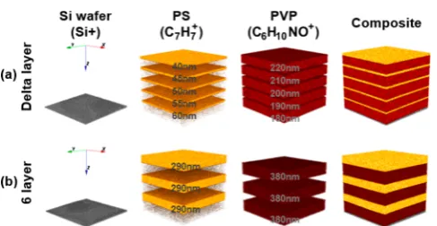
Four different samples were prepared using spin-coating and depth profiled using ToF-SIMS (summarized in Table SI.1, Supporting Information). The variable thickness sample was prepared as a comparison to theδ-layer samples previously prepared by Shard et al.21Thin PS layers (between 40 and 60 nm) were deposited between thick PVP layers (between 180 and 220 nm). The thickness of the PVP and PS layers was varied as a function of layer deposition number. This was controlled by using a faster/slower deposition spin-speed, which results in thinner/thicker layers, respectively. The sample contained 10 layers and was used to determine the ToF-SIMS capability to measure layer thickness. A similar 10 layer sample was also prepared without variation in the layer thickness. This “δ-layer constant thickness sample”had PVP and PS layers that weredPVP= 200±1 nm anddPS = 50±1 nm thick, respectively. The“6 layer sample”had thicker PS layers (PVP and PS layer thickness weredPVP= 379±5 nm anddPS= 286±1 nm, respectively) and was used to test the ability of the sputtering source to sputter through thick layers of PS. Finally, a“50 layer sample”(PVP and PS layer thickness weredPVP = 328±7 nm anddPS= 288±1 nm, respectively) was prepared to test the ion beam’s ability to sputter through a sample with a total thickness of 15.40±0.04μm. All of the samples were prepared on silicon wafers except the 50 layer sample, which was prepared on a glass slide. The 50 layer sample was prepared differently because it was used in a previous study of the optical properties of polymer multilayers.1
A“home-built”self-nulling ellipsometer was used to determine the thickness of layers within the samples. The refractive index of the PVP and PSfilms were measured asnPVP= 1.516±0.001 andnPS= 1.586± 0.001, respectively, using the ellipsometer. A fitting program was written to calculate the thickness of the polymerfilms using a modified optical transfer matrix method. Single layer samples were prepared using the same spin-speed and concentration as the spun-cast layers in the multilayer experiments and theirfilm thickness values measured using ellipsometry. Measurements of bilayer samples of PVP and PS revealed that differences in thefilm thickness were negligible whether spun-cast on top of silicon or the alternate polymer layer. It was concluded that the thickness of single layerfilms is indistinguishable from the thickness of a film/layer in a multilayer sample that was deposited using similar conditions.
ToF-SIMS Depth Profiling.A ToF-SIMS IV (ION−TOF GmbH, Münster, Germany) instrument was used to acquire depth profiles from the multilayerfilms. The instrument was equipped with a Bi/Mn liquid metal ion gun (LMIG) and an argon gas cluster ion gun, which were operated in the dual beam mode. Details of the ion gun design are given by Kayser et al.26A 5 keV Ar2000+cluster ion beam was used for sputtering. This source produces a distribution of cluster sizes that is characterized by the resolution parameterΔn/n≈30% (wherenis the number of argon atoms in a cluster). The Ar2000+sputtering beam (target current of 1.1 nA) was rastered over the sample with a spot size of∼25μm. A 25 keV Bi3+analysis beam (pulsed target current of 0.10 pA) was used to analyze the central area between sputtering pulses. An electronflood gun was also employed for charge compensation, using approximately 20 μA, 20 eV electrons over an oval area with a characteristic length of 3 mm. Both of theδ-layer samples and 6 layer sample were measured with the Ar2000+beam rastering over a 350× 350μm area and the Bi3+beam rastering over a 100×100μm area. Whereas the Ar2000+beam rastered over a 400×400μm area and the Bi3+beam rastered over a 200 × 200μm area during the 50 layer sample measurement. Data acquisition and subsequent data processing and analysis were performed using SurfaceLab 6 (ION-TOF).
Multivariate Data Analysis.MVA was used on the depth profile data obtained from the polymer multilayerfilms. This took the form of principal component analysis (PCA). This technique was used to analyze the chemical composition of the samples. The data sets were analyzed by considering each ToF-SIMS depth profile scan as a separate data set with data processing using PLS_Toolbox (version
5.2, eigenvector Research, Manson, WA) for Matlab (Mathsworks, Inc., Natick, MA). Ion spectra peaks were automatically selected using SurfaceLab 6. The ion intensity data was exported, normalized to the total counts and mean centered. An initial estimate of the number of significant principal components was obtained from the eigenvalue data.
Layer Thickness Calculation.Single layer PVP and PS calibration samples were spun-cast onto silicon wafers with thickness valuesdPVP = 206±1 nm anddPS= 219±1 nm, respectively (measured using ellipsometry). These samples were depth profiled and the position of the polymer−silicon interface was determined. Different regions were studied in order to minimize any observable differences in measured sample topography. This can be caused by sample alignment, layer topography/roughening, changes in sample density and/or impurities which change the sputter rate. This was compensated for by dividing the surface of the sample into 5 regions of interest (ROI), which each contained between 10% and 20% of the total surface area. Ion signals were preferentially selected to identify PVP, PS and silicon layers. The C7H7+(m/z= 91) and Si+(m/z= 28) ions were attributed to the PS and silicon layers, respectively. The presence/absence of PVP was determined from the measured intensity of the C6H10NO+(m/z= 112) ion. Each interface in the depth profile data wasfitted to the following error function27 using software written in Matlab (Math-works)
μ σ
= ⎡ + − +
⎣
⎢ ⎛⎝⎜ ⎞⎠⎟⎤ ⎦ ⎥
f d( ) A d C
2 1 erf 2 (1)
whereAis the maximum amplitude of the depth profile band,dis the dose of the ion cluster,μis the interface that is the transition point between two layers, 2σgives the width of the interface andCcorrects for any background ions which may have been detected.
The thickness (d) and interface widths were calculated using an average of measurements from the 5 ROIs. Standard error of the measurements from the 5 ROIs was used to calculate the associated error of the layer thickness and interface width. Each layer thickness was calculated by measuring the dose needed to sputter from one interface (μ1) to the next (μ2) using thefitting program twice for each interface. The ion cluster dose used to sputter through each calibration sample was compared with the ellipsometryfilm thickness measure-ment. Hence, the sputtering yield volumes PVP and PS layers were (11.66 ± 0.10) and (14.77 ± 0.18) nm3/ion, respectively. The interface width was calculated by multiplying 2σby the sputtering rate of the preceding layer. Two bilayer samples of PVP and PS (where the order of the top and bottom layers are different for each sample) were prepared and measured using both ellipsometry and ToF-SIMS depth profiling to determine whether the sputter rate varies. The thickness of the PVP and PS layers in the bilayer samples weredPVP= 206±1 nm anddPS= 219±1 nm, respectively (which is the same thickness as the single layer samples) when measured using ellipsometry. ToF-SIMS measurements of the PVP layer thickness as the lower or upper layer were 205±1 and 208±2 nm, respectively. Similarly, the ToF-SIMS measurements of the PS layer thickness as the lower or upper layer were 227±3 and 221±1 nm, respectively. These minor differences could be due to nonuniform sample topography that cannot be accounted for at present.
■
RESULTS AND DISCUSSIONChemical Composition.The depth profiling capabilities of the argon cluster source provide detailed information about the chemical composition of the polymer multilayer systems studied here. This was confirmed by using principal component analysis (PCA) on a 6 layer sample. PCA is a statistical procedure that transforms a selection of possibly correlated variables (in this case ion intensity values) into linearly uncorrelated variables called principal components. The scores plot for principal components 1 and 2 is shown in Figure SI.2 (Supporting Information). The PVP and PS layers are clearly differentiated by their distribution with respect to “principal
component 1”(PC1, which captured 99.90% of the variance), as expected for a two component system. Most of the significant ions that were identified are observed to differentiate the PVP and PS layers as being of high or low significant variance respectively on PC1, as illustrated in the loadings data shown in the Supporting Information (Figure SI.3). In addition to PCA of these polymer multilayer systems, further investigation was conducted in the form of a search for common contaminants observed in the ToF-SIMS data, such as sodium and potassium. However, these contaminants were not observed in significant quantities. Furthermore, the depth profile data was also used to look for secondary ions which do not correspond to the PS, PVP or Si profiles or which express heterogeneous lateral distributions. However, no such secon-dary ions were found, indicating that the spatial distribution of chemical species is homogeneous within each layer.
Depth Profiling.Samples of alternating PVP and PS layers were depth profiled using the argon sputtering beam. A comparison of positive and negative polarity data showed similar results for the systems studied here. Both polarities could have been used for sample analysis, as a broad range of ions which are unique to each layer were detected. For the sake of brevity, only the positive data will be presented in the depth profile and reconstructed three-dimensional (3D) model data (see the 3D Reconstruction section). The specific layers of PS, PVP and the silicon wafer were identified using the C7H7+(m/z
= 91), C6H10NO+ (m/z = 112) and Si+ (m/z = 28) ions,
respectively.28
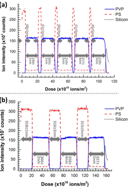
Plots of the measured secondary ion intensity for PVP, PS and Si, as a function of the incident sputtering ion dose, are shown in Figure 1. Panel a shows the depth profile curves for the“δ-layer variable thickness”sample. Thefirst layer at the top of the sample was PS, which had afilm thickness of 60±1 nm. Each underlying PS layer had a 5 ± 1 nm reduction in film thickness. Hence, the PS layers had thickness values of 60±1, 55±1, 50±1, 45±1 and 40±1 nm from top to bottom of the sample, which were determined by measuring comparable single layerfilms with ellipsometry. Likewise, thefirst PVP layer (2nd layer from the top) had an initial thickness of 180±1 nm. Each underlying PVP layer had a 10 ±1 nm increase in film thickness. The thickness of the PVP layers from top to bottom were 180±1, 190±1, 200±1, 210±1 to 220±1 nm. In each case, the layer thickness of a given polymer was controlled by varying the angular speed of the spin coater during deposition of the layers. Panel b in Figure 1 shows the depth profile of the “6 layer” sample. All of the PVP layers had a thickness of dPVP = 379 ± 5 nm and the PS layers had a
thickness ofdPS= 287±1 nm, as measured by ellipsometry. Both depth profiles in Figure 1 show that the ion intensities were maintained at constant levels throughout profiling. The total thickness of the δ-layer variable thickness and 6 layer samples were approximately 1.3 and 2.0μm, respectively. These samples were much thicker than those analyzed in previous systems such as theδ-layers reported by Shard et al., which had an approximate total thickness of 0.4μm.22This demonstrates the ability of the argon cluster ions to sputter through thicker samples and also demonstrates that these multilayers have potential applications as ToF-SIMS calibration samples.
A 50 layer sample was depth profiled in order to investigate the argon cluster source’s capability to successfully sputter through a very thick sample. Figure 2 shows the depth profile of a small region of interest over a 35 × 35 μm surface area. Measuring a smaller surface area reduces the magnitude and
increases the “noise” of the secondary ion intensity. The ion intensity of the peaks attributed to both of the polymers
decreases as the sample is being sputtered. However, it is still possible to clearly distinguish between separate PVP and PS layers throughout the sample.
Layer Thickness. The thickness of the polymer layers (previously shown in Figure 1a) were compared with the appropriate sputter rate for each layer. Each layer thickness was calculated using eq 1. Figure 3 shows a comparison of the
ToF-SIMS (using the δ-layer sample) and ellipsometry (using comparable single layer samples) layer thickness measurements. The ellipsometry and ToF-SIMS thickness values are within 11% of one another, with differences ranging between 2.3 and 31.2 nm.
ToF-SIMS measurements showed a decrease in the PS layer with respect to increasing layer number in the variable layer thickness sample (Figure 3). The thickness of the PVP layers in this sample did increase, but the ToF-SIMS values differed from the values obtained from ellipsometry measurements. The largest difference between the ToF-SIMS and ellipsometry measurements was observed in the third PVP layer (6th layer of the sample), which was 19± 2 nm. These discrepancies are thought to originate from sample topography, which cannot be easily accounted for within the sample regions analyzed by ToF-SIMS depth profiling.
3D Reconstruction. Three-dimensional (3D) secondary ion images were reconstructed from the depth profile data. These images chemically map the spatial variations in the distribution of the polymers throughout the multilayer systems. The 3D reconstruction images of the δ-layer and 6 layer samples are shown in Figure 4. This chemical imaging showed the homogeneous PVP and PS distribution within the respective PVP/PS alternating layers. These images are thought to be an accurate visualization of the spatial distribution of polymers in these multilayer samples. This would have been previously unobtainable using alternative sputter sources due to the problematic PS layers. The PVP/PS multilayers were ideal for this type of study due to the inclusion of the challenging PS layers and controllable layer thickness throughout. Although the x- and y-direction are shown to scale, the z-direction is presented according to ion dose and as such does not reflect the discrepancy between the sputter rates of PS and PVP.
Figure 5 shows a 3D chemical image of a 10 layer PVP/PS sample. The thickness of the PVP and PS layers are constant at
dPVP= 200±1 nm anddPS= 50±1 nm. The parallel view of
[image:4.625.71.295.66.388.2]this sample reveals a defect present after the third layer (top to bottom). This defect has a diameter that is approximately 10 Figure 1.Positive ion depth profiles of alternating PS/PVP multilayers
using 5 keV Ar2000for sputtering and 25 keV Bi3for analysis of a) aδ -layer sample with variable thickness (5 PS -layers of 68, 61, 56, 51 and 45 nm thick interdigitated with 5 PVP layers of 190, 204, 219, 217 and 218 nm thick and b) a 6 layer sample with constant thickness (3 PS layers of 318, 316, 315 nm thick interdigitated with 3 PVP layers of 366, 358 and 357 nm thick). In each case PS, PVP and silicon wafer data were extracted from the C7H7+, C6H10NO+and Si+ion intensities, respectively. The layer thickness values obtained from ToF-SIMS measurements are given in the panels.
[image:4.625.325.564.151.292.2]Figure 2.Positive ion depth profile of a 50 layer PS (blue) and PVP (red) sample for a constant thickness system (PS = 288±1 and PVP = 328±7 nm) using 5 keV Ar2000for sputtering and 25 keV Bi3for analysis. This is a depth profile from a 35×35μm ROI. The PS, PVP and glass slide substrate layers were identified using the C7H7+, C6H10NO+and Si+ions, respectively.
Figure 3.Film thickness measurements of the layers from the variable thickness sample shown in Figure 1a. The PVP and PS layer thickness values were measured using ToF-SIMS and ellipsometry.
[image:4.625.68.291.503.660.2]μm wide. Film thickness and interface measurements are less accurate after sputtering beyond the occurrence of the defect due to it offsetting all of the subsequent depth profile bands. The measured thickness of the third PVP layer (from top to bottom) is thicker, which displaces the positions of the interface for the underlying layers. This also broadens the interface widths as the polymer layers blend into one other. The defect is also present when using other secondary ions which represent the PVP and PS layers. No contaminants were detected in the defect regions of the ToF-SIMS data or elsewhere for the PVP/PS samples. This demonstrated the Ar cluster ion source’s ability to isolate defects in these PVP/PS calibration samples which would be difficult to observe using other techniques.
[image:5.625.325.560.59.231.2]Figure 6a shows the 3D chemical image of the 50 layer sample over a 200 × 200 μm area (images have not been corrected for lateral shift owing to thefixed 45°geometry of the analysis ion beam). Some of the 3D chemical image is distorted by defects that are thought to originate from the substrate of the sample. Defects at the substrate will offset the position of subsequent layers analyzed creating the effect observable in Figure 6a.
Specific areas of the 3D image showed well-defined layers of PVP and PS, such as the 35×35μm ROI shown in Figure 6b. The depth profile of the ROI (shown in Figure 6c) revealed a clear separation between the PVP and PS layers. This data demonstrates that the ToF-SIMS argon cluster ion beam setup was capable of sputtering through and analyzing large polymer structures (severalμm in thickness) as well as detecting defects. It is worth noting that the thickness and complexity of this sample was significantly larger than those measured in similar studies. To our knowledge, there have been no other studies of a multilayer system of a comparable thickness that have been measured using ToF-SIMS.
■
CONCLUSIONSPreviously unavailable insights into PVP/PS multilayers have been obtained using ToF-SIMS with argon cluster depth profiling. The depth profile data illustrate proportionate sample compositions up to relatively high depths of ≤15 μm while retaining useful ion intensities, thereby enabling detailed sample chemical analysis. Information regarding the 3D chemical homogeneity of the samples has also been successfully extracted. Important details regarding variations in the structure of these systems and potential defects have been observed that could lead to improvements in sample manufacture and development. The potential for the use of PVP/PS multilayers as calibration samples for ToF-SIMS has also been demon-strated.
■
ASSOCIATED CONTENT*
S Supporting InformationTable containing the full layer thickness details for the four multilayer systems investigated in this study, the principal component analysis study of a 6 layer sample, and loadings for PC1 and PC2 from PCA of PS/PVP alternating layers. This material is available free of charge via the Internet at http:// pubs.acs.org.
■
AUTHOR INFORMATIONCorresponding Author
[image:5.625.60.304.63.189.2]*D. J. Scurr. E-mail: [email protected]. Figure 4.Reconstructed 3D positive ion images (200×200μm area)
from a depth profile of PS/PVP spun-cast multilayers using a 5 keV Ar2000beam for sputtering and 25 keV Bi3for analysis. These images show (a) 5×PS = 40−60 nm and 5×PVP = 180−220 nm and (b) 3
×PS (290 nm)/3×PVP 380 nm multilayer systems.
[image:5.625.105.541.642.729.2]Figure 5.Reconstructed 3D positive ion images (200×200μm area) from a depth profile of a 10 layer PS/PVP spun-cast multilayer (5×PS = 50 and 5×PVP = 200 nm) exposing a layer defect. These ion images were collected using 5 keV Ar2000for sputtering and 25 keV Bi3for analysis.
Figure 6.Positive ion images from a depth profile of the 50 layer sample using 5 keV Ar2000for sputtering and 25 keV Bi3for analysis, (a) reconstructed 3D image of total ion signal over a 200×200μm surface area, (b) plan view of panel a showing regions of low intensity caused by defects. A 35×35μm defect-free region of interest is shown and (c) reconstructed 3D images from the region of interest showing clear definition between the PVP and PS layers.
Notes
The authors declare no competingfinancial interest.
■
REFERENCES(1) Bailey, J.; Sharp, J. S. Thin Film Polymer Photonics: Spin Cast Distributed Bragg Reflectors and Chirped Polymer Structures. Eur. Phys. J. E: Soft Matter Biol. Phys.2010,33, 41−49.
(2) Bailey, J.; Sharp, J. S. Infrared Dielectric Mirrors Based on Thin Film Multilayers of Polystyrene and Polyvinylpyrrolidone. J. Polym. Sci., Part B: Polym. Phys.2011,49, 732−739.
(3) Forrest, S. R. The Path to Ubiquitous and Low-Cost Organic Electronic Appliances on Plastic.Nature2004,428, 911−918.
(4) Drury, C. J.; Mutsaers, C. M. J.; Hart, C. M.; Matters, M.; de Leeuw, D. M. Low-Cost All-Polymer Integrated Circuits.Appl. Phys. Lett.1998,73(1), 108−110.
(5) Park, H. Y.; Kim, K.; Kim, D. Y.; Choi, S. K.; Jo, S. M.; Jang, S. Y. Facile External Treatment for Efficient Nanoscale Morphology Control of Polymer Solar Cells Using a Gas-Assisted Spray Method.
J. Mater. Chem.2011,21, 4457−4464.
(6) Sariciftci, N. S.; Smilowitz, L.; Heeger, A. J.; Wudl, F. Photoinduced Electron Transfer from a Conducting Polymer to Buckminsterfullerene.Science1992,258(5087), 1474−1476.
(7) Mora-Huertas, C. E.; Fessi, H.; Elaissari, A. Polymer-based Nanocapsules for Drug Delivery.Int. J. Pharm.2010,385(1−2), 113− 142.
(8) Kawaguchi, H. Functional Polymer Microspheres. Prog. Polym. Sci.2000,25, 1171−1210.
(9) Adawi, A. M.; Cadby, A.; Connolly, L. G.; Hung, W. C.; Dean, R.; Tahraoui, A.; Fox, A. M.; Cullis, A. G.; Sanvitto, D.; Skolnick, M. S.; Lidzey, D. G. Spontaneous Emission Control in Micropillar Cavities Containing a Fluorescent Molecular Dye.Adv. Mater.2006,18, 742− 747.
(10) Geoghegan, M.; Hadziioannou, G.Polymer Electronics; Oxford University Press: Oxford, U. K., 2013.
(11) Imae, T.; Kanaya, T.; Furusaka, M.; Torikai, N.Neutrons in Soft Matter; Wiley and Sons: New York, 2001.
(12) Willis, B. T. M.; Carlile, C. J.Experimental Neutron Scattering; Oxford University Press: Oxford, U. K., 2009.
(13) Havelund, R.; Licciardello, A.; Bailey, J.; Tuccitto, N.; Sapuppo, D.; Gilmore, I. S.; Sharp, J. S.; Lee, J. L.; Mouhib, T.; Delcorte, A. Improving Secondary Ion Mass Spectrometry C60n+ Sputter Depth Profiling of Challenging Polymers with Nitric Oxide Gas Dosing.Anal. Chem.2013,85(10), 5064−5070.
(14) Mahoney, C. M.; Fahey, A. J.; Gillen, G.; Xu, C.; Batteas, J. D. Temperature-Controlled Depth Profiling in Polymeric Materials Using Cluster Secondary Ion Mass Spectrometry (SIMS). Appl. Surf. Sci.
2006,252, 6502−6505.
(15) Nieuwjaer, N.; Poleunis, C.; Delcorte, A.; Bertrand, P. Depth Profiling of Polymer Samples Using Ga+ and C
60+ Ion Beams.Surf. Interface Anal.2009,41, 6−10.
(16) Adawi, A. M.; Connolly, L. G.; Whittaker, D. M.; Lidzey, D. G.; Smith, E.; Roberts, M.; Qureshi, F.; Foden, C.; Athanassopoulou, N. Improving the Light Extraction Efficiency of Red-Emitting Conjugated Polymer Light Emitting Diodes.J. Appl. Phys.2006,99, 054505.
(17) Millers, R.; Tuccitto, N.; Torrisi, V.; Niehuis, E.; Licciardello, A. Chemical Effects in C60Irradiation of Polymers.Appl. Surf. Sci.2006, 252, 6509−6512.
(18) Sjovall, P.; Rading, D.; Ray, S.; Yang, L.; Shard, A. G. Sample Cooling or Rotation Improves C60 Organic Depth Profiles of Multilayered Reference Samples: Results from a VAMAS Interlabor-atory Study.J. Phys. Chem. B2010,114, 769−774.
(19) Miyayama, T.; Sanada, N.; Iida, S.; Hammond, J. S.; Suzuki, M. The Effect of Angle of Incidence to Low Damage Sputtering of Organic Polymers Using a C60 Ion Beam.Appl. Surf. Sci.2008,255 (4), 951−953.
(20) Kozole, J.; Wucher, A.; Winograd, N. Energy Deposition during Molecular Depth Profiling Experiments with Cluster Ion Beams.Anal. Chem.2008,80(14), 5293−5301.
(21) Shard, A. G.; Havelund, R.; Seah, M. P.; Spencer, S. J.; Gilmore, I. S.; Winograd, N.; Mao, D.; Miyayama, T.; Niehuis, E.; Rading, D.; Moellers, R. Argon Cluster Ion Beams for Organic Depth Profiling: Results from a VAMAS Interlaboratory Study.Anal. Chem.2012,84
(18), 7865−7873.
(22) Shard, A. G.; Foster, R.; Gilmore, I. S.; Lee, J. L. S.; Ray, S.; Yang, L. VAMAS Interlaboratory Study on Organic Depth Profiling. Part I: Preliminary Report.Surf. Interface Anal.2011,43, 510−513.
(23) Wagner, M. S. Molecular Depth Profiling of Multilayer Polymer Films Using Time-of-Flight Secondary Ion Mass Spectrometry.Anal. Chem.2005,77(3), 911−992.
(24) Lee, J.; Gilmore, I.Surface Analysis: The Principal Techniques, 2nd ed.; John Wiley & Sons, Inc.: New York, 2009.
(25) Scurr, D. J.; Horlacher, T.; Oberli, M. A.; Werz, D. B.; Kroeck, L.; Bufali, S.; Seeberger, P. H.; Shard, A. G.; Alexander, M. R. Surface Characterization of Carbohydrate Microarrays. Langmuir 2010, 26
(22), 17143−17155.
(26) Kayser, S.; Rading, D.; Moellers, R.; Kollmer, F.; Niehuis, E. Surface Spectrometry Using Large Argon Clusters.Surf. Interface Anal.
2013,45, 131−133.
(27) Seah, M. P. Resolution Parameters for Model Functions Used in Surface Analysis.Surf. Interface Anal.2002,33, 950−953.
(28) Briggs, D.; Brown, A.; Vickerman, J. C. Handbook of Static Secondary Ion Mass Spectrometry (SIMS); Wiley: Chichester, U. K., 1989.