from the screen on the nitriding layer formation. ASPN experiments were carried out using a DC plasma-nitriding unit. The sample was placed on the sample stage in a floating potential (bias-off) and a cathodic potential (bias-on). The screen, which was SUS 316L expanded metal with 38% open area ratio, was mounted on the cathodic stage around the sample stage. Nitriding was performed in a nitrogen-hydrogen atmosphere with 25% N2 + 75% H2 for 18–180 ks at 673 K under 200 Pa by the ASPN process. After nitriding, the nitrided samples were examined using scanning electron microscopy, X-ray diffraction, Vickers microhardness and glow discharge optical emission spectroscopy. From the surface observation of the nitrided sample, deposits were observed on the top surface of the sample nitrided with bias-off whereas deposits were not on that nitrided with bias-on. The nitrogen-expanded austenite (S phase) was formed on the surface of both samples. Layer thickness of the S phase increased with increasing the nitriding time. Additionally, the degree of an increase of the layer thickness of the S phase nitrided with bias-on was approximately 2.5 times greater than that nitrided with bias-off. This result suggests that the ASPN treatment with bias-on is effective for the increase of the nitriding layer thickness. [doi:10.2320/matertrans.M2016209]
(Received June 8, 2016; Accepted August 4, 2016; Published September 2, 2016)
Keywords: active screen plasma nitriding, nitriding layer, austenitic stainless steel, expanded austenite, bias, surface deposits
1. Introduction
The nitriding process is widely used to improve the tribo-logical properties and wear resistance and corrosion resis-tance of steel and titanium alloys. In commercial nitriding system, the uptake of nitrogen is performed in various envi-ronments, such as salt bath, gas and glow-discharge plasma. Each technology has associated advantages and disadvan-tage. Plasma nitriding is becoming increasingly popular due to its high nitrogen potential, short treatment time and low environmental impact.1–7) However, the components to be
treated are subjected to a high cathodic potential in traditional DC plasma nitriding (DCPN), which results in the production of plasma directly on their surface. As a result, edge effect, arcing and hollow cathode occur.8)
Recently, considerable interest has been paid to alternative nitriding processes such as active screen plasma nitriding (ASPN), through-cage plasma nitriding, and cathodic-cage plasma nitriding.9–23) These processes offer the advantage of
completely eliminating that defection associated with con-ventional plasma nitriding processes, as the plasma is pro-duced on the screen and not directly on the samples.9–11)
These processes can be used to treat polymers that are non-conductive materials.24–26)
Stainless steel has good corrosion resistance because the chromium containing in the steel forms a passive layer on the steel surface. Therefore, stainless steel has various applica-tions, such as in chemical and nuclear industries, and it is also used as a structural material. However, plasma nitriding at temperatures between 723 and 823 K decreases the corrosion resistance. Since chromium in steel reacts with nitrogen to form chromium nitride, it decreases the concentration of chromium in the matrix, which is necessary for the formation
of stable passive layers. Therefore, low temperature plasma nitriding was used. The plasma nitriding treatment of austen-itic stainless steel below 723 K forms a nitriding layer called an S phase (expanded austenite), which improves the surface hardness without decreasing the corrosion resistance.27–34) In
a previous study, S phase was formed by ASPN.9,16,17,33,35) A
recent research suggested that a deposited layer was formed on the sample surface during ASPN.36–38) However, little
in-formation has been reported on the effect of the surface de-posits on the nitriding layer formation during ASPN process. In this study, austenitic stainless steel SUS 316L was nitrided with a floating potential (bias-off) and a cathodic potential (bias-on) of ASPN process to investigate the effect of surface deposits from the screen on the nitriding layer formation.
2. Materials and Experimental Procedure
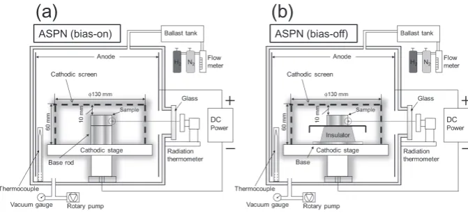
The sample material used in this study was austenitic stain-less steels SUS 316L (chemical composition (mass%) of 0.013% C, 0.18% Si, 1.69% Mn, 0.034% P, 0.012% S, 16.75% Cr, 12.02% Ni, 2.00% Mo, and the balance being Fe). The stainless steel sample was 20 mm in diameter and 5 mm in thickness. Prior to nitriding, the stainless steel sample sur-face was mechanically ground with 150–2000-grit SiC, finely polished with 0.05 µm diamond paste, ultrasonically degreased in acetone, and dried in air. The preconditioned sample was then placed in a nitriding furnace for further ASPN treatment. ASPN experiments were conducted with a DC plasma-nitriding unit (NDK, Inc., Japan, JIN-1S). The ASPN setups are shown in Fig. 1. In Fig. 1(a), the sample was also placed on the stage but without insulative material and thus connected directly to the cathodic potential and conse-quently the plasma formed both on the samples and active screen (bias-on). In Fig. 1(b), the sample was placed at a floating potential (bias-off) on an insulative material (ceramic crucible) and isolated from the cathodic cage screen and the *1
Corresponding author, E-mail: [email protected] *2
anode.
The screen material used in this study was SUS 316L of expanded metal mesh with open area of 38%, formed into a cylinder of 130 mm diameter and 60 mm height. The distance between the screen and the sample was 10 mm. The screen was thoroughly degreased ultrasonically in acetone. After placing the sample on the sample stage, the chamber was evacuated to a pressure of approximately at 8 Pa. Then, nitro-gen and hydronitro-gen were introduced into the chamber, and a DC bias voltage was supplied. Nitriding was performed in a nitrogen–hydrogen atmosphere with 25% N2 + 75% H2 for
18–180 ks at 673 K under 200 Pa by the ASPN process. After nitriding, the DC supply was switched off, and the sample was cooled to room temperature in the furnace. The nitriding temperature was monitored with a radiation thermometer po-sitioned at the sample.
The phase structure on the nitrided surface was determined by θ–2θ X-ray diffraction (XRD; RIGAKU, Japan, RINT-2550V). The entire area of the top surface of nitrided samples was analyzed by XRD. The nitrided microstructure and com-positional analysis of nitrogen were examined with a scan-ning electron microscope (SEM; JEOL, Japan, JSM-6060LV) and a glow discharge optical emission spectroscopy (GD-OES; Horiba, Japan, GD-profiler2). For this, cross sec-tions of each sample were first cut using a low-speed saw, then polished, and chemically etched.
3. Results and Discussion
The external appearance of the nitrided samples was visu-ally examined, as shown in Fig. 2. Appearance of sample sur-face treated by the ASPN processing has uniformly and the edge effect and arcing were not observed. The surface gloss was lost as the processing time increased. Furthermore, in the ASPN process, the samples were heated to the treatment tem-perature by the heat radiation from the active screen, which promoted a higher homogeneity of temperature in the treated samples.10)
Figure 3 shows the XRD patterns of the SUS 316L treated by the ASPN processing. In Fig. 3, XRD pattern of the SUS 316L treated by the ASPN processing identified S phase (ex-panded austenite),27,28) which is considered to be a
supersatu-rated solid solution of nitrogen in austenite. For the longer nitriding time, peaks of S phase were shifted to lower angle
compared with the XRD pattern of the sample nitrided for 18 ks with bias-on of the ASPN process. Moreover, CrN was also identified on the samples treated with the bias-off. The diffraction angle of the S phase nitrided with the bias-on was lower than that nitrided for the bias-off. This result shows that solid solution of nitrogen in the S phase nitrided with the bi-as-on was more than that nitrided for the bias-off.
Figure 4 shows surface morphologies of the sample treated with bias-on and bias-off of the ASPN process. Polygonal particles were observed on the surface nitrided with the bi-Fig. 1 Schematic illustration of ASPN setups: (a) bias-on and (b) bias-off.
Fig. 2 External appearance of SUS 316L samples nitrided for 18–180 ks at 673 K with bias-on and bias-off of the ASPN process.
[image:2.595.129.465.68.221.2] [image:2.595.307.549.268.373.2] [image:2.595.306.546.429.612.2]as-off while they were not observed for the bias-on. This re-sult indicates that in the bias-on, plasma forms on the screen and the sample and sputtering on the sample always occurs. Therefore, no deposited layer formed with the bias-on of the ASPN. These polygonal particles are considered to be surface deposits.36,37) These particles became coarser with increasing
nitriding time. This result indicates that the FeN deposition increased with increasing treatment time, and these deposited particles grew.10,11)
The microstructures of the cross sections of the samples treated by the ASPN process are shown in Fig. 5. An S-phase layer, which was slightly corroded by oxalic acid, was ob-served on the both sample surfaces.27,28) Moreover, a
deposit-ed layer was also observdeposit-ed on the S-phase layer for the ASPN (bias-off) whereas not for the ASPN (bias-on). This deposited layer is considered to be composed of S phase and CrN, as shown in Fig. 3. Several researchers have proposed a model of sputtering and deposition during ASPN.10,13,19,20,35) In
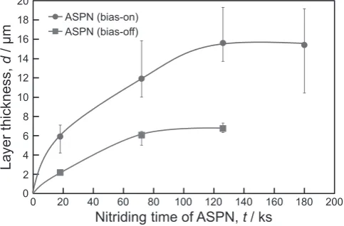
this model, nitrogen ions sputter the screen, the sputtered ma-terials form nitrides with nitrogen in the plasma, and nitrides deposit on the sample s surface. It is thought that this model can be adapted to the bias-off of the ASPN process in this study. The uniformity of the thickness of the S-phase layer nitrided with bias-off of the ASPN process was observed while that with bias-on was not observed. In addition, the thickness of the S-phase layer nitrided with bias-on was much thicker than that nitrided with bias-off. Figure 6 shows the effect of the nitriding time of ASPN on the layer thickness. The thickness of the nitriding layer of the S phase increased with increasing nitriding time. The thickness of the nitriding
layer of the S-phase for the ASPN (bias-on) was much thicker than that for the ASPN (bias-off), as shown in Fig. 5. The degree of an increase of the layer thickness of the S phase nitrided with bias-on was approximately 2.5 times greater than that nitrided with bias-off. This result indicated that ni-trogen diffusion was not suppressed because of no deposited layer on the sample surface nitrided with bias-on of the ASPN process. It is thought that the formation of the nitrides and NH radicals increased because of the increase of region of plasma formation. That is, the plasma forms on both the screen and the sample for the ASPN (bias-on). The growth rate of the S-phase layer nitrided with bias-off was smaller than that of the deposited layer nitrided with bias-off of the ASPN process, as shown in Figs. 5 and 6. This result suggest-ed that the depositsuggest-ed layer suppresssuggest-ed the formation of a ni-triding layer.
Figure 7 shows the GD-OES profiles of the SUS 316L samples nitrided for 126 ks at 673 K with bias-on and bias-off of the ASPN process. These were obtained for nitrogen, oxy-gen, iron, chromium and nickel. In Fig. 7(b), the profiles ob-tained suggest a surface region approximately 5 µm thick, the deposited layer, composed of nitrides. This is consistent with the XRD result, as shown in Fig. 3. Oxygen element was de-tected in the deposited layer for the bias-off, as shown in Fig. 7(b). Saeed et al., showed that iron oxide Fe3O4 was
formed on the sample surface treated for the bias-off of the ASPN by XRD.20) It is thought that for the bias-off of the
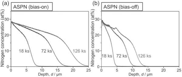
ASPN process in this study, fine deposits formed without sputtering on the sample surface and very fine particles in the deposited layer resulted in the oxidation of much grain boundaries. Figure 8 shows the GD-OES profile of nitrogen concentration of the SUS 316L sample nitrided for 126 ks at 673 K with bias-on and bias-off of the ASPN process. In Fig. 8(b), a profile of nitrogen concentration shows that the duplex structure of the surface region consisted of the depos-ited layer on the top followed by the nitriding layer (S-phase layer) in the sample with bias-off of the ASPN process. In addition, concentration gradient of nitrogen in the deposited layer and the nitriding layer was observed. That is, the inter-face between the deposited layer and the nitriding layer (S-phase layer) was observed. Figure 9 shows GD-OES pro-Fig. 4 Surface morphology of SUS 316L samples nitrided for 18–180 ks at
673 K with bias-on and bias-off of the ASPN process.
Fig. 5 Cross-sectional SEM images of SUS 316L samples nitrided for 18– 180 ks at 673 K with bias-on and bias-off of the ASPN process.
[image:3.595.306.548.73.232.2] [image:3.595.48.291.76.190.2] [image:3.595.49.290.257.372.2]files of nitrogen concentration for SUS 316L samples nitrided for 18, 72, and 126 ks at 673 K with bias-on and bias-off of the ASPN process. In Fig. 9(a), nitrogen-concentrated depth increased with increasing nitriding time with bias-on of the ASPN process. In Fig. 9(b), nitrogen concentration at the in-terface between the deposited layer and the nitriding layer decreased with an increase of the nitriding time with bias-off of the ASPN process whereas that at the top surface was al-most same. This result indicates that nitrogen diffusion for the formation of the nitriding layer (S-phase layer) beneath the deposited layer was suppressed by decreasing the nitro-gen concentration at the interface between the deposited layer and the nitriding layer. These results suggested that a deposit-ed layer on the nitriding layer formdeposit-ed by the ASPN process (bias-off) impeded the growth of the nitriding layer. On the
other hand, nitrogen concentration at the top surface was not changed with increasing nitriding time with bias-on of the ASPN process. This result suggested that nitrogen diffusion was not suppressed because the nitrogen was supplied direct-ly from the plasma into the sample surface. This resulted in the deeper nitriding layer was formed on the sample with bi-as-on compared with bias-off of the ASPN process. It is thought that the ASPN treatment with bias-on is effective for the increase of the nitriding layer thickness.
4. Conclusions
Austenitic stainless steel SUS 316L was treated with bi-as-on and bias-off of the ASPN process to investigate the de-posited layer formed on the sample surface. The results sug-Fig. 8 GD-OES profiles of nitrogen concentration for SUS 316L samples nitrided for 126 ks at 673 K with bias-on (a) and bias-off (b) of the ASPN process.
Fig. 9 GD-OES profiles of nitrogen concentration for SUS 316L samples nitrided for 18, 72, and 126 ks at 673 K with bias-on (a) and bias-off (b) of the ASPN process.
[image:4.595.144.445.73.208.2] [image:4.595.150.447.262.389.2] [image:4.595.148.448.428.555.2]This research was financially supported by a Kansai Uni-versity Grant-in-Aid for progress of research in graduate course, 2015.
REFERENCES
1) Y. Sun and T. Bell: Mater. Sci. Eng. A 140 (1991) 419–434.
2) M. Samandi, B.A. Shedden, D.I. Smith, G.A. Collins, R. Hutchings and J. Tendys: Surf. Coat. Tech. 59 (1993) 261–266.
3) A. Nishimoto and K. Akamatsu: Plasma Process. Polym. 6 (2009) S306–S309.
4) H. Dong: Int. Mater. Rev. 55 (2010) 65–98.
5) M. Egawa, N. Ueda, K. Nakata, M. Tsujikawa and M. Tanaka: Surf. Coat. Tech. 205 (2010) S246–S251.
6) W. Li, X. Li and H. Dong: Acta Mater. 59 (2011) 5765–5774.
7) S. Adachi and N. Ueda: Thin Solid Films 523 (2012) 11–14.
8) C. Alves, Jr., E.F. da Silva and A.E. Martinelli: Surf. Coat. Tech. 139 (2001) 1–5.
9) C.X. Li, T. Bell and H. Dong: Surf. Eng. 18 (2002) 174–181.
10) C. Zhao, C.X. Li, H. Dong and T. Bell: Surf. Coat. Tech. 201 (2006) 2320–2325.
11) C. Alves, Jr., F.O. de Araujo, K.J.B. Ribeiro, J.A.P. da Costa, R.R.M. Sousa and R.S. de Sousa: Surf. Coat. Tech. 201 (2006) 2450–2454.
12) A. Nishimoto, A. Tokuda and K. Akamatsu: Mater. Trans. 50 (2009) 1169–1173.
13) S. Corujeira Gallo and H. Dong: Vacuum 84 (2009) 321–325.
14) A. Nishimoto, T.E. Bell and T. Bell: Surf. Eng. 26 (2010) 74–79.
15) Y. Li, L. Wang, D. Zhang and L. Shen: J. Alloy. Compd. 497 (2010)
22) A. Yazdani, M. Soltanieh and H. Aghajani: Vacuum 122 (2015) 127– 134.
23) M. Naeem, M. Shafiq, M. Zaka-ul-Islam, Naila Nawaz, J.C. Díaz-Guillén and M. Zakaullah: Mater. Lett. 181 (2016) 78–81.
24) A.P. Kauling, G.V. Soares, C.A. Figueroa, R.V.B. de Oliveira, I.J.R. Baum, C. Giacomelli and L. Miotti: Mater. Sci. Eng. C 29 (2009) 363– 366.
25) X. Fu, R.L. Sammons, I. Bertoti, M.J. Jenkins and H. Dong: J. Biomed. Mater. Res. B Appl. Biomater. 100B (2012) 314–320.
26) G. Kaklamani, J. Bowen, N. Mehrban, H. Dong, L.M. Grover and A. Stamboulis: Appl. Surf. Sci. 273 (2013) 787–798.
27) Z.L. Zhang and T. Bell: Surf. Eng. 1 (1985) 131–136.
28) K. Ichii, K. Fujimura and T. Takase: Technol. Rep. Kansai Univ. 27 (1986) 135–144.
29) X. Li, Y. Sun and T. Bell: Z. Metallk. 90 (1999) 901–907.
30) Y. Ueda, N. Kanayama, K. Ichii, T. Oishi and H. Miyake: Surf. Coat. Tech. 193 (2005) 50–54.
31) J. Buhagiar, X. Li and H. Dong: Surf. Coat. Tech. 204 (2009) 330–335.
32) M. Chemkhi, D. Retraint, A. Roos, C. Garnier, L. Waltz, C. Demangel and G. Proust: Surf. Coat. Tech. 221 (2013) 191–195.
33) Y. Li, Z. Wang and L. Wang: Appl. Surf. Sci. 298 (2014) 243–250.
34) F.A.P. Fernandes, T.L. Christiansen, G. Winther and M.A.J. Somers:
Acta Mater. 94 (2015) 271–280.
35) A. Nishimoto, T. Matsukawa and H. Nii: ISIJ Int. 54 (2014) 916–919.
36) P. Hubbard, J.G. Partridge, E.D. Doyle, D.G. McCulloch, M.B. Taylor and S.J. Dowey: Surf. Coat. Tech. 204 (2010) 1145–1150.
37) H. Nii and A. Nishimoto: J. Phys. Conf. Ser. 379 (2012) 012052.