VM-88S1 Graphics Processor Manual
VM-8851 Graphics Processor Manual
MULTIBUS Intel trademark Copyright VMI1984
Vermont M icrosystems, Inc. One Main Street, POB 236 Winooski, Vermont 05404
While. to the best of our knowledge. this manual contains accurate information and graphics, it is subject to change without notice. VMI cannot be held responsible for any errors. omissions. or misinformation that may appear in this manual. Changes made to the information contained in this document will be incorporated in new editions of this publication.
VM-8851 Graphics Processor Manual
Sec t ion
1 2 2.1 2.2 2.3 2.3.1 2.3.2 2.4
2.5
2.6
3
3.0 3.1 3.2
3.3
3.4
3.5 3.6
5
5.1
5.2
5.3
5.4
5.5
5.6
Table of Contents
Description
Introduction
VM8851 Architecture Processor Section
Scanne r Sec t ion MULTIBUS Intertace
Programmed I/O Master Mode Display RAM
Timing and Control Output Section Bardware Operation
overview
Processor Section Host Interface
Scanner and Start Address Table Display RAM Timing and Control Di splay RAM
Output Section
Firmware Design Considerations
~irmware Initialization
Address Assignment Memory Organization
Display. RAM Organization Display RAM Access
LUT Programming
Appendix A Appendix Bl Appendix C
Related Documents Processor Schematics Componen t Lis t
1-- 1
2-1 2-1 2-1 2-4 2-4 2-4 2-6 2-8 2-8 3- 1 3-1 3-1 3-2
3-4
3-5 3-8 3-9 5-1 5-1 5-1
5-4
5-4
5-5
VM-8851 Graphics Processor Manual
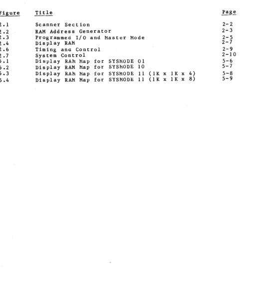
[image:5.620.55.564.95.692.2]List of Illustrations
Figure Title pa~~
----2.1 Scanner Section 2-2
2.2 RAM Address Generator 2-3
2.3 Programmed I/O and Master Mode 2-5
2.4 Display RAM 2-7
2.6 Timing ana Control 2-9
2.7 System Control 2-10
5.1 Display RAN Map for SYSMODE 01 5-6
5.2 Display RAM Map for SYS~lODE 10 5-7
5.3 Display RAM Map for SYSMODE
11
( 1 K x 1 K x 4) 5-8VM-8851 GraphiCS Processor Manual
1 - Introduction
The VM-b851 Graphics Processor delivers n~xt-generation graphic~
on a single MULTIBUS compatible board. The Intel 8088 CPU.
operating at 8 MHz with up to 200 Mbytes local memory and up to two Mbytes image memory, provides considerable flexibilty in complex applications requiring highly independent graphics
processing. For less complex applications. 8088-based
applications code installed directly onto the single-board system
provides the basis for stand-alone sys.tem capability. The
graphics processor generates displays of up to 256 simultaneous
colors chosen from a 4096 color palette. Flexible image RAM
organization permits the choice of a high-resolution image (up to
lK x lK) or multiple, image buffers. High-performance features
such as 60 Hz refresh rate, pixel pan within a lK x lK image
space, 128 independent display windows, and hardware zoom offer signi1icant enhancements beyond previous graphics processor
implementations. Output consists of RGB video with selectable
sync.
The graphics processor provides flE:xible MULTIBUS interfaces. A 128-byte FIFO buffers MULTIBUS to graphics processor commands and
data when in slave moue. Master mode capability permits DMA
operation or stand-alone operation. MULTIBUS 24-bit addresses
are generated and detected. The functionality of the graphics
processor expands by adding expansion modules on the SBX connector.
A hig h-l eve..l, easy- to-use gr aph ic s la nguag e, INTERACTTM, run s on the graphics processor to provide a user accessible method for
generating complex graphics images. INTERACTTM resides in a
section of the graphics processor PROM space and responds to high-level commands from the MULTIBUS interface or from on-board applications code.
This manual provides a description of the graphics hardware architecture and operation and firmware design considerations.
Section 2 describes the architecture 01 the graphics processor.
Section 3 explains the theory of operation of the hardware. Section 5 covers the board hardware from the programming point of
view. This information enables the user to maximize board use
for any particular application. Section 5 also includes
necessary hardware and software descriptions for debug~ing
user-written 80bb software.
VM-8851 Graphics Processor Manual
2 - Processor Architecture
2.1 - CPU Local Memory
An 8 - MHz 8 0 ~ 8 m i c r 0 pro c e s s 0 r run n i n g i n "M AX mod e" for m s the
basis of the CPU section. The board aesign of local memory
allows various combinations of PROM and RAM. Jumpers supply
appropriate connections to flag the board for the current
configuratIon. (Refer to the configuration section to determine
the proper Jumper placement for signaling the contents of each socket.)
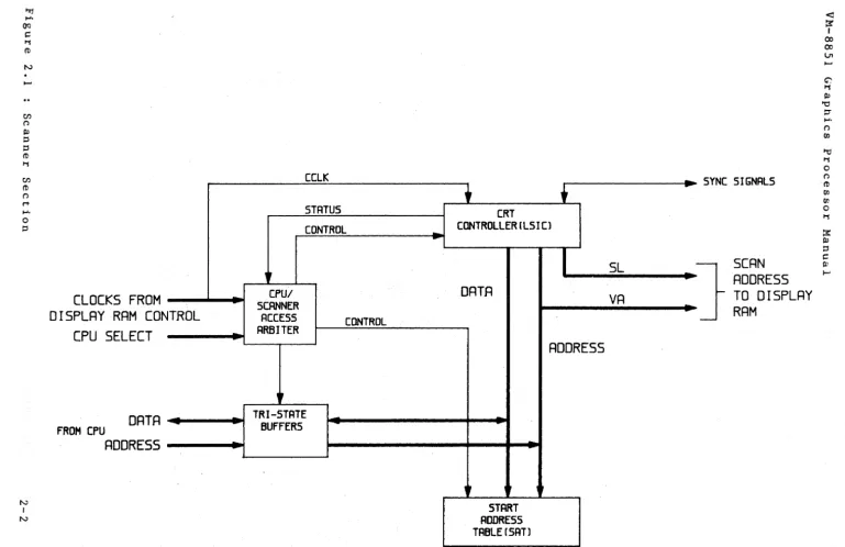
2.2 - Scanner Section
The scanner section supports the hardware ZOOM and PAN functions by producing the proper addresses to scan, though i t does not
directly address memory. Instead, the RAM address generator
latch holds the scanner address during a valid period. This
address remains latched until applied to memory at a later time
Both the scanner and the CPU share the VA and VD buses (for
addresses and data respectively). Using these buses the CPU can
program the scanner. To achieve this goal, the CPU f i r s t gains
control of tne scanner so that the scanner ceases to send out its
own signals. The processor then applies addresses on the VA bus
and data on the VD lines to program the scanner.
The scanner and CPU also shar e 256 bytes of RAM (U39.U40). The
scanner, accessing during horizontal retrace, can only read
information stored in RAM. The CPU accesses this RAM space
during vertical retrace and can perform both read and write functions.
This RAM space contains the starting address table usea by the
scanner during i t s operation. Every four raster lines in a
display constItutes a group. for each group, the RAM stores a
starting address in a table format. These addresses can exist
anywhere withIn a 16-pixel boundary of display RAM. The CPU
programs the starting address table to structure the memory and
to determine which part of the display to scan out. At every
fourth line, the scanner accesses the starting address table during horizontal retrace to determine the starting address for
the next group. The scanner reads in the next value then applies
the address during visible line time Between th~ CPU and the
scanner, U38 arbitrates access to the starting address table and
the scanner. Re1er to figures 2.1 and 2.2.
N
en
(!) ('l
r-t ~.
o
::l
N I N
DATA ... -.... - -...
~fROM CPU
ADDRESS - - -...
~TRI-STATE
BUfFERS
START
ADDRESS
TABLE {SATl
r---4-~
SYNC SIGNALS
SCAN
ADDRESS
TO DISPLAY
RAM
<
~ I 00 00 I.n
....
"'0
.,
o
('l (!)
C/l C/l
[image:8.802.12.781.51.548.2]N
ROW
CPU ADDRESS
<
4: 19)
COL
COLUMN ADDRESS
6
DISP/CPU
..
-..
-..
LRTCH
,I
SCANNER
TIS
ROW
LRTCH
ADDRESS
SCANNER
COLUMN
TIS
ADDRESS
LATCH
TIS
CPU ROW
LATCH
ADDRESS
CPU COLUMN
TIS
ADDRESS
LATCH
-MUX
5
~
HUX
S j
SCANNER HOST
SIGNIfICANT
RDDRESS TO
CONTROL
MULTIPLEXED
ADDRESS
BUS A
MULTIPLEXED
ADDRESS
BUS B
<:
~
I
0) 0)
\Jl
~.
Ci t; III '0
::-....
n
C/l
'"
t; 0n
ID
C/l C/l
0 t;
~
III
::l
c::
III
VM-8851 Graphics Processor Manual
2.3 - MULTIBUS Interface
The VM:-8851 supports two standard typt!s of host interface
simultaneously. Programmed I/O provides high-speed.
bi-directional data transfer between the host and the VM-8851 with
an extremely simple interface. DMA operation allows greater
sys t em throughput by fre e i ng the ho s t proc e s so r fo r ot he r tas ks
while the VM-8851 fetches data from system memory. With an
optional SBX serial interface, board data can also be transmitted
to the VM-8851 from any RS232 compatible device. Refer to figure
2.3 for further inlormation in r~ading the next sections.
2.3.1 - Programmed I/O
Using an o-bit-wide data transfer, the programmed I/O section allows the ho'st to communicate through the MULTIBUS to the
on-board C~U, an Intel 8088. Signals coming onto the board pass
f i r s t through the bus receiver, composed of four 64 x 5 FIFOs.
This configuration produces a 128 x (8
+
2) bit FIFO, used by thehost to read status and to send data to the board. The design
reserves eight bits for data. The remaining two bits function as
signal bits. They identify DMA command data and distinguish
those commands from INTERAL1TM commands. (Refer to the INTERACTTM Command Language Manual for more i nfor ma t io n.)
The address deCOder consists of a large jumper array. Two 20-pin
header sockets l i e offset from each other on the board. This
deSIgn conserves space. These two positions can derive five
commonly used addresses: 24-bit, 20-bit, l6-bit, l2-bit, and
8-b i t . In a l l these cases. jumpers select the eight most
significant bits which will feed to the address comparator
(ALb520). This chip compares the data with the eight bits held
in the dip switch to produce the host select signal (HSTSEL). The PAL 20LlO further decodes the signal to determine the action requested.
2.3.2 - DMA Section
The VM-8851 enacts DMA transfers using Master Mode. In the DMA
section, the bus arbiter makes all requests of the bus for DMA
transactions and handles the priority levels. The bus controller
generates I/O signals as determined by th~ CPU. The CPU
initiates a transfer by sending an address. The three address
latches hold this value while the CPU sends data to each
respective address. The host software determines the block
accessed and controls the read/write operations sent to the
board. Also through the host software, the latch controls access
to memory pages.
When the LPU wants to access certain ranges of adaresses, the DMA
section interprets these inquiries as off-board requests. It
then disables all local devices and converts to Master Mode ~n
the bus. Following this transfer of control, the 8289 produces a
.
VolH
-
o III ::I c:l.N I
V'1
ADORES
FROM MULTI BUS
CONTRO
S
L
XACK
. MULTIBUS DATA
ADDRESS
MULTIBUS
CONTROL
...
-
--~
--HOST
ADDRESS
DECODER
-
I
HOST
DATA
OUTPUT
~I""'-
REGISTER
•
TAG
~,
BITS
19 BIT
--
X 126 WOIW
FIFO
HOST
DATA
INPUT
INTERRUPT MASK
CHIP SELECTS
READY STATUS
HOST
STATUS
REGISTER
I""'-
--
l-'"-FIFO STATUS
BUFFERS
-1
r~
INTERRUPT
CONTROL
LOCAL
STATUS
REGISTER
BUS
ARBITER
f--+-I
-LOCAL CHIP
SELECTS
LOCAL INTERRUPT
(PBINTJ
MULTI6US
INTERUPT
I"C'Jt-I
o
n
ro
en en
o
t-I
LOCAL DATA
BUS~LOCAL ADDRESS
BUS
L
B
OCAL CONTROL
US
III ::I
c::
VM-8851 Graphics Processor Manual
bus request signal. On receiving a bus grant
using local CPU data and control.
It drives the bus
The upper six bits supplied on MULTIBUS drive the latch. The
board can then access any of the 16K blocks available. However,
to cross a 256K boundary, the CPU must reprogram the latch.
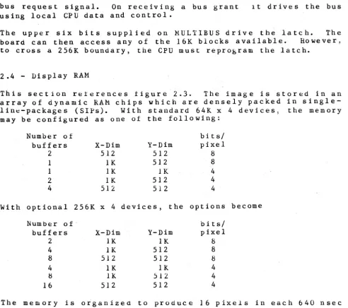
2.4 - Display RAM
This section relerences figure 2.3. The image is stored in an
array of dynamic RAM chips which are densely packed in
single-lin~-packages (SIPs). With standard 64K x 4 devices, the memory
may be configured as one of the following:
Number of bits/
buffers X-Dim Y-Dim pixel
2 512 512 8
1 1K 512 8
1 lK lK 4
2 1K 512 4
4 512 512 4
With optional 256K x 4 devices, the options become
Number of bits/
buffers X-Dim Y-Dim pixel
2 lK lK 8
4 1K 512 8
8 512 512 8
4 1K 1K 4
~ 1K ~12 4
16 512 512 4
The memory is organized to produce 16 pixels in each 640 nsec
cycle. These pixels are then shifted out to the video output
section at a rate of 40 nsec per pixel. The CPU can access the
display RAM at any time without disturbing the display output. When the CPU writes to display RAh the address and data are latched briefly to synchronize to the display cycle without making the CPU wait.
Display RAh data output is transformed through a programmable
look-up table into binary values which drive video DACs. The
design contains four separate look-up tables of 256 x 12 bits.
These LUTs may be selected by the CPU to implement an
instantaneous transtormation of the displayed image. Display
modes which use only four bits per pixel have only two selectable
llok-up tables. In those conligurations, one bit of the scan
address drives the look-up table select to distinguish which nibble of the display data should be mapped to output.
[image:12.630.56.548.68.504.2]~ ~.
00
c::
t"$ CD
N
"'"
t ;
~.
rJl
"0
...
III
'<
~
:t>
l:?:
N
I
-...J
LATCHED 0<0:7>
HAD A
RAS
CAS
WRITE
CONTROL
CPU DATA
BUS
BLANK
,
,
I I
~ I
I I --.
I I I
-
II I I I I
32 BIT
-
LATCH
HUX
<:
~
I 00
0:
\J1
-,
G') t"$
III 'e
::r
--
MADB
~.n
rJl
"d
--
RAS
t"$0
n
CD rJl
-
CAS
rJl0
t"$
~
III
.WRITE
;:lc::
III
...
32 BIT
LATCH
-
CONTROL
HUX
REGISTER
-
CLOCKPIXEL BUS
-VM-8851 Graphics Processor Manual
2.5 - Timing and Control
The major structure of the timing and controi section is depicted
in figures 2.5 and 2.6. The clock generator produces various
divisions and phases of the 50 lYiliz master clock. The dot clock
has a frequency of 25 Mliz~ so video data output is updated every
40 n sec. An 0 the rim po r tan t per i 0 d i s the " c h a r act e r" per i 0 d, 6 40
nsee or 16 pixels. This frequency defines the resolution with
which the scanner addresses display RAM.
CPU accessible latches drive the major control lines, making many
operational choices software-selectable. These options include
seven display RAM write modes ranging from one to 16 pixels, pan
displacement. blanking~ nibble write-protect. bank selection, and
look-up table (LUT) selection. System mode selection is also
accessible to the CPU and refers to the logical structure of
display RAM and the LUT. Many dynamic control signals are
directly affected by these software-defined controls.
Much of the timing and control circuitry is implemented in programmable logic (PLA or PAL) due to the complex interrelations
of these signals. A programmable logic sequencer generates the
display RAM control signals and arbitrates, between the CPU and
the scanner~ access to the the display RAM. When the CPU writes
to display RAM) the address and data are latched so that the CPU
can execute further instructions without waiting for the display
RAM cycle to complete. This process cannot be done with read
cycles~ but very few common operations require reading the dis pIa y RAM.
Selection of individual pixels or groups of pixels from a
"character" ot 16 pixels is accomplished by a combination of
timing and device selection. Timing is essential, because nibble
mode operation implies that different addresses are accessible at di11erent times in the cycle.
Individual pixel panning is accomplished by selecting the
appropriate phase of the clock to latch sync and blanking
slgnals. This technique effectively skews the displayed data on
the screen. Since the monitor cannot instnatly adjust to this
change in sync phase~ the operation is done only at the beginning
of vertical blanking.
Two-power zoom operation alters the control sequences to run most
parts at half-speed. Clock signals to the scanner, however, must
remain at full speed and not shift in phase at the transition to
zoom mode. This condition requires that the transition be
synchronized to the scanner clock.
2.6 - Output Section
Storage registers contain all the output LUT information. The
board provides an option of two D/A converters (DACs):
monochrome or color (T0444).
.
0\
ZOOM
CPURe
CPUWR
DISPLAY SELECT
MOOE<0:3>
•
LATCHED
A<~:3>
P.AN CONTROL
ZOOM REQUEST
SYNC 6 BLANKING
FROM SCANNER
---...
....
HASTER
OSCILLATOR
511JHHZ
CPU
ACCESS
CONTROL
58 MHZ
-
GENERATOR
CLOCK
-MULTI
PIXEL
WRITE
CONTROL
-
RAS,
CAS,
AND OTHER
MEMORY
TIMING
---
-VIDEO
r----.
CONTROL
~
--
~FOR
SYSTEM
SYNCRON IZATION
DOTCLOCK(25 MHZ)
12.5 MHZ CLOCK,
PHASE 1
12.5 MHZ CLOCK,
PHASE 2
WRITE LINES
GRAS<0:3>
CAS<~:3>
MISCELLANEOUS
LATCHING SIGNALS
TO MAINTAIN DATA
PIPELINE TO DISPLAY
ZOOM
SIGNALS TO
CONTROL SYNC,
BLANKING INTERFACE
TO SCANNER
SCANNER
CLOCKS
<
~
I
00 00
V1
...
t<.l
....
I» 'tl
::r
....
n
OJ
I-tI
....
0
n
(b
OJ OJ 0
....
~
I»
1:1 ~
III
N
.
"-J
~
cpU
CONTROL
m
RD,VR
rot CD S (":) o ::l rot 1'1 o
~
HODEL
N
I
-
oDISPLAY SELECT
R<0:3>
SCANNER HOST
SIGNIFICANT
ADDRESS
VR rTE SELECTS
CPU 0<0:7>
SYNCRON I
ZATI ONREGISTER
,
CPU
-
ADDRESS
-
LATCHED
SIGNALS
ICPU
SYSTEH
DATA
DESCRIBING
LATCHED
SIGNALS
-
SIGNALS
-SYSTEH
HODE
LDGIC
-HAINTAINS
CDHPAT IB IL rTY
-VrTH
256KNIBBLE HODE
DRAMS
-MULTIPLEXED
RDDRESS 8 FOR
256K DRRMS
CPURD,CPUWR
DISPLAY SELECT
LRTCHEO RDDRESS
<0:3>
MODE<0:3>
LUT BANK CONTROL
CPU BLANK
COLUHN
ADDRESS 6
FOR
641( DRAMS
PAN CONTROL
ZOOM
<
~ 1 00 00 VI....
(j) 1'1 ~ "C ~...
n m '"C1 1'1 0 n CD m m 0 1'1 ~ ~ ::lc:
~ ~ASSORTED HARDWARE
CONTROL SIGNALS
VM-8851 Graphics Processor Manual
Each look-up table (LUT) receives four bits of information. One
byte contains data for the red and green LUTs, and a nibble
transfers blue LUT data. In the color system all three LUTs send
four bits of color information as output. The DACs convert this
information into RGB signals. In the monochrome system, the red
and green LUTs supply the first eight bits as input data for the
DAC. The blue LUT contributes two bits which the DAC interprets
as reference white and 10% overbright. These non-linear values
directly affect the information detined by the other eight bits.
When the CPU asserts the reference white line, the output
increases to full intensity. The 10% overbright line high causes
the data input to increase its intensity by 10%. The monochrome
video output appears on the green output signal used for color. This method capitalizes on the sync-on-green capability.
VM-8851 Graphics Processor Manual
3 - Hardware Operation
3.0 - Overview
This section describes the theory of operation of the VM-8851
g rap h i c s pro c e s s 0 r • E a c h sub sec t ion coni t a ins d eta i 1 e d
descriptions 01 each of the major blocks in the VM-8851
architecture. Please refer to the schematics in appendix B while
readin~ these ~ections as the text often refers to a speci~ic
schematic sheet. Signal names are printed in upper case, t.g.
XACKL. Compon~nts are indicated by a single letter followed by a
n u m be r, e. g. U 6 2 • A" U" ref e r s to a n i n t e g rat e d c i r cui t, "R" to
a resistor, "C" to a capacitor, "D" to a diode,
"p"
to a J,llaleconnector,
"J"
to a female connector, and "W" to a jumper.3.1 - Processor Section
With a 24 kHz crystal, Y13, the clock generator, U21 outputs an 8
MHz CLK. U2 also controls the generation of CPU wait states
through the RDY output pin. The AENI input to U2 is hel~ high
when the CPU has to wait to access display RAM, the scanner. the
s t a r t address table, or the SBX board. For SEX connector
transfers requiring wait states, a low signal on MWAITL will
prevent an AEN1 signal.
When display RAM is accessed, pin 13 of U9 goes low until the
display RAM controller returns DISPRDYH. AEN1 is forced high
causing the processor to ·wait. Likewise, when either the scanner
or the start-address table (SAT) is accessed, pin 19 of U10 goes
high. This change causes AENI to go high until the scanner/SAT
arbiter, U38, activates SCNRDYL. U9-13 also goes low when an off
board access occurs, producing a wait state until the bus
arbiter, U26, activates the signal AEN2L. AEN2L acts like the
select input of a multiplexor. When high, its normal state, the
AEN1 input of U2 is active. When AEN2L is low. the AENI input is
i g nor e Q , but the RD Y 2 in put d r i v en by the bus X. A C K Lsi g n ai, i s
used to prod uce RDY.
The r e s i s t o r kl, capacitor Cl19, inverter UI07, and open collector driver UI09 combine to provide the power-on reset
function. A MULTIBUS reset signal INITL will also reset the
clock generator, thereby resetting the CPU, U1.' The CPU, U1,
operates in maximum mode (MIN/MXL=GND.) The bus controller, U3,
decodes CPU status signals SO, 51, and S2 to create MRDCL, MWTCL,
and AMwCL control signals. U3 also generates the address latch
enable signal (ALE) and the data buffer control signals DEN and
DT/RL. During an interrupt acknowledge cycle, U3 generates
INTAL. The input CEN disables U3 during an off-board access
cycle.
Durin~ the interrupt acknowledge cycle, the interrupt controller,
U4, accepts up to seven level-sensitive interrupt inputs on IRO
through IRS P 1 u s SIN T and P BIN T 1 and is sue s a v e c tor with
VM-8851 Graphics Processor Manual
appropriate priorities to each of data bus lines DO through D7.
Jumper matrix WI routes the incoming interrupts to the
appropriate interrupt line.
Jumper matrix W2 determines the selection of one of eight
MULTIBUS interrupts for input and two of eight interrupts for
output. The interrupt PBINT2 or the CPU-generated interrupt
MBINT route through open collector driver UI09 to any of the
eight MULTIBUS interrupt lines. An o~tionally-attached floating
point processor supplies interrupt line MINT. (Refer to iSBC 377
module for details in Intel manual 142887-001.)
3.2 - Host Interface
Pages five and six of the scematics show the MULTIBUS host interface section which consists of both programmed I/O and DMA
interfaces. Both of these interfaces are fully compatible with
the separate interface boards used on the VM-8850A and may be used simultaneously.
The board typically uses eight bytes of MULTIBUS address space
and may be con fig u r e C1 for 8 - , 16 - , 2 0- , or 24 - bit add res s
decoding, either memory or I/O mapped. Pins 2 and 3 of W22
select the type of address while pins 4 through 9 provide six
bits of address comparative data. W5 and W6 select between
memory mapped and I/O mapped operation. Refer to section X.X f·or
address select ion.
FPLAs U25 and U13 act almost like multiplexors in that Ahl and AMO select which set of six address lines to compare against the
six inputs from jumper W22. The six most significant bits in
each address type are thus compared with the jumpers, while the
less significant bits are usually required to be zero. Any
arbitrary address may be selected, however, by reprogramming U25
and U13. When the address matches, U13 produces HSTSEL. Another
PLA, U24, receives HSTSEL along with ADRLO-ADRL2 and the read and
write control signals. U24 decodes these to produce the
following chip select signals.
Use address 0 for programmed I/O data transfer. A read at this
address produces DTAENL, enabling U22 to drive the data bus, while a write produces SI, which shifts data in from U14 to the
FIFO, UI5-UI8. TAGI and TAG2 will equal 0 for programmed I/O
transfers.
A read at address 1 produces STSENL.This signal, used in both programmed I/O and DMA operations, enables U21 onto the data bus.
A w r i t e t 0 add res s I p rod u c esC ~1 D L C HL w h i c h c I 0 c k s U 3 3 t 0 I a t c h
data bits 0 and 2 to form the host's interrupt enable masks. U23 also uses CMDLCHL to latch data bit 6, which constitutes the reset command.
Addresses 2 and 3 are not used. Addresses 4 through 7 are used
for DMA operation and are write only. A" write to any of these
VM-885l Graphics Processor Manual
addresses produces SI, to shift the data into the FIFO; DMACMDL, which signals U23 that DMA 1s being written; and the tag bits
TAGI and TAG2. The tag bits identify the type of data in the
FIFO. This information is deduced from the address to which the
data was written. As noted above, a tag value of 0 denotes
programmed 1/0 data. Value 1 (address 4) is the low byte of a
DMA control block adoress. Value 2 (address 5 or 6) indicates
the high byte(s), and value 3 (address 7) marks the DMA reset
command. An access to any of the valid addresses described above
also produces XACKL immediately to signal the bus master that the
transi~r can proceed. U24 produces TXRDY as long as 1) the FIFO
is not full, or half-full, depending on the setting of w20, and
2) a reset (warm start) is not in progres~. Depending on the
state of the host's interrupt enables (from U33) plus the states or TXRDY and RXRDY, U24 produces PBINT2, which may be connected through W2 to one of the eight MULTIBUS interrupt vectors.
U23 proouces a variety of status information. When the host
sends a reset command (CMDLCHL active and D6 equal t o l ) . i t
activates CGBRST. The CPU clears this signal by producing PBCSI
with AO equal to O. Similarly, RXRDY is set when the local CPU
pro d u c e s P B C S 2 (1 a t chi ng d a t a in to, U 2 2) and c 1 ear e d w hen the ho s t
pro d u c e s D T A EN L (r e a din g d a t a fro m U 2 2) • Ac t i vat in g the bus
reset signal INITL also clears both RXRDY anO CGBRST. DRDY is
high whenever OR from U18 is high unless CGBRST is high. HFULL
is active low when IRhF from U18 is low, unless CGBRST is low. HFULL low indicates a half-full condition in the FIFO.
The signals DMAChDP and DMAPRSNT are similar. They indicate the
presence of DMA data in the FIFO and are set when DMACMDL is
activated. DMAPRSNT serves as a status bit to the local
cpu.
Itis cleared automatically when the DMA reset command is read out
of the FIFO. DMACMDP, a status bit to the host, is cleared when
the CPU produces PBCSI with AO equal to 1.
The two most significant bits (MSBs) latcheo by U28 (refer to
sheet 6 of the schematics) are MASKl and MASK2. In U23, these
bits condition the generation of PBINTI as follows. CGBRST
active produces the interrupt regardless of mask bits. If MASK2
is high, RXRDY low produces the interrupt. (RXRDY low indicates
that the host has read the last data sent.) If MASKI is high,
the interrupt is produced by either HFULL active or by tagged
data (DMA data) available at FIFO output. The local CPU rea~s
these status bits through U2U and FIFO data through U19.
Once DMA data is retrieved from the FIFO, the local CPU performs the DMA operation using the MULTIBUS master mode hardware on
sheet 6 of the schematics. U26 arbitrates bus control, producing
AEN2L when bus mastership is aquired. U27 decodes the CPU status
lines SO-52 to generate MRDCL, MWTCL, IORCL, IOWCL, the data bus
enable, and the data direction control signals. U28 is a latch
which is written before an off-board (master mode) access is
made. This latch holos the upper six bits of the MULTIBUS
address since the
8088
CPU has only 20 address lines, two ofwhich are used to decode the off-board request. U29-U31 drive
VM-88S1 Graphics Processor Manual
the MULIBUS address bus with 18 bits from the CPU and six bits
from U28. U32 buffers the data bus. The board supports only
8-bit data transfers. Reier to section X.X to determine the
appropriate configuration of W7-W9 for a specific application.
US2 divides FCLK, the SO hHz master clock, by five to produce a
10 Mhz signal. This signal is buffered through U41 to drive
ThNMhZ to the SBX connector and BCLKL if W21 is closed. The
other half of U41 buffers various status bits to be read by the
local CPU. Bit 3 indicates the presence of an SBX module. Bit 2
connects to W23 but has no defined meaning at this time. Bit 1
reflects the state of LPENSW. Bit 0 is reserved for future
expansion.
3.3 - Scanner and Start Address Table (SAT)
The CRT9007, U36, produces sync, blanking, and other control signals in addition to the addresses applied to the display RAM. This programmable LSI device is oriented to alphanumeric displays but is readily adapted to the high performance graphics in the
VM-88S1. The signal SCCLK, buffered by UII0, clocks U36 at a 640
nsec period. Each such period produces a new address which
ultimately provides 16 pixels to the display, that is, 40 nsec
per pixel. The low six bits of the video address bus, VAO-5,
address up to 64 such "characters", or 1024 pixels. The 8LO-2
lines form the next three bits of address, the three leqst
s i g n i f i c a n t b i t s of the y-coordinate. These b i t s simply
1ncrement during each horizontal retrace. The first line at the
top of the screen, however, may load SL from an internal register
t o e f f e c t sin g 1 e l i n esc roll • V A 6 - 1 2 for m the roe m a i n d e r 0 f the
y-coordinate for a total address range of 1024 x 1024.
At the beginning of each 8-line "window", U36 produces DRB and a
s p e cia 1 add res s fro man in t ern a I r e g i s t e r • Th i s pro c e s s c au s e s
data from the start address table (SAT) to drive the VD bus. In
this way, U36 reads the SAT to determine the address in display
RAM of the next window. This address is a "character" address,
that is, i t has a resolution of 16 x 8 pixels. The CPU writes to
the SAT to control which portion of RAH is displayed. Thus one
level of panning can be effected by simply modifying entries in
the SAT. As noted earlier, finer vertical pan (scroll) is done
by preloading the 8L address at the beginning of each frame. Finer horizontal pan is acomplished by skewing tha sync and
blanking signals slightly. Refer to section X.X.
A two-power zoom operation is likewise performed at the character
level. UU36 increments the memory address on every other clock,
and 8L increments every other line. Further manipulation of
individual pixels for zoom operation is described in section X.X.
The signal LPENIN connects tfr U36 in order to latch the character
address at the time of light pen strobe. The CPU then reads the
address from U36. The sync outputs are "open drain" and may be
driven with external sync signals by wiring W11 and W12 pin 2 to
VM-88S1 Graphics Processor Manual
4.
sync sync
This configuration causes U36 to synchronize to the external
source. CRD2 and CRD3 prevent conflicts between the two
drivers.
U38 is a programmable logic sequencer (FPLS) which arbitrates
access between the CPU, the scanner (U36), and the SAT (U39
&
U40). When the CPU asserts SCNRSL, U38, by leaving SCNRDYL high,
causes the CPU to wait until the scanner is not using the VA and
VD buses. U38 then enables the CPU to drive these buses through
U34 and U3S, producing SCNRDYL and the chip select for U36.
Likewise, when the CPU asserts STBLSL, U38 times the transaction and produces the chip select and write enable to U39 and U40.
The scanner also reads the SAT. U38 determines this information
from DRB and VLT and produces the SAT chip select. Since the
scanner operates in real-time mode, i t generally has higher
priority than the CPU.
U37 latches the sync and. blanking signals in two stages. The
f i r s t stage simply synchronizes them with the high-speed
operation of display kAM. The second stage is clocked by a phase
variable signal to effect horizontal pan. Before either stage
occurs, composite blanking, CBH, is combined with CPUBLANK in
UII3 and then fed through UII8. Refer to sheet 8 of the
schematics. By setting pin 9 of U68, UII8 shortens the unblanked
period to either 512 or 640 pixels as selected by the CPU. This
step is necessary because in panning, part of the last character
scanned is not displayed. The scanner, though, cannot assert CBH
before it has completed scanning a line.
UII7 combines horizontal and vertical sync to produce composite
sync. UIOS then buffers those signals and provides both
polarities to WII and WI2 for user selection.
3.4 - Display RAM Timing and Control
This section covers primarily the circuits shown on sheets 8 and 9 of the schematics.
U42 latches the CPU-generated signals AMWCL, RDL, and DISPL to
synchronize them with the display RAM arbitration circuit. This
synchronization avoids dynamic hazards. DISACCH also loops
through U42 again, producing DDISACCH which clocks U72. This
delay is neeaed because CAD6, which is latched by U72, is
produced from LAI, which in turn is latched by DISACCH. U42 also
synchronizes MADA8 and MADB8. These multiplexed address lines
are used with the optional 256K x 4 RAM chips. U48 produces
these lines as a function of CPU bank select, display bank
select, DISP/CPU, and ROW.
U 4 3 i s a d u a I 4 - bit I a t c tl, e a c h h a I f h a v i n gAO - 3 a s i n put s • The
f i r s t latch is clocked on DISACCH to latch the four LSBs of
address on display RAl"1 access. These bit'S are called LAO-3 and
determine which pixel(s) in a group (character) of 16 is desired. The same clock signal latches the other address lines in U71 and
VM-8851 Graphics Processor Manual
U72 (sheet II) and data in U44. These buses are latched so that,
on write operations, the CPU need not wait for the arbiter to complete the operation.
U45 is a latch trig~ered by chip select PZBSML. It is used to
control panning via PANO-3, display blanking via CPUBLANK, and
zoom via ZOOMB. The CPU must set these signals at the
appropriate time to avoid display glitches, generally during vertical retrace.
NHBSLL clocks U46 to latch four different sets of control
Signals, each two bits wide. NO-I are nibble write~protect masks
applied to display RAE write operations. CPUBSO-l select which
of four possible 5I2K byte display RAN banks is used when the CPU
accesses display RAM. With 64K x 4 RAt--. chips, these bits should
always equal 00. DISPBSO-I likewise select which bank is
displayed and should equal 00 with 64K x 4 RAN chips. SYSMODEO-l
selects the display RAM configuration. Essentially, SYSMODEI
selects 64K x 4 or 256K x 4 (0 or I respectively), while SYSMODEO selects lK x 512 organization or lK x lK organization (0 or 1
respectively). These signals are decoded along with other
address and timing signals by U48 to produce the multiplexed
address lines mentioned above, LS8, WRITEN, and CAD6. LS8 and
LS9 (from U47) select which set of look-up tables are used in the
output section. In lK x lK x 4 organization, denoted by SYSMODE
01 or 11 and PIXDEPTH=I), LS8 is driven by VA12SYNC so that when the scanner addresses the second bank, i t really receives data
from the first bank. The look-up table is conditioned to use the
upper nibble of data instead of the lower. In other modes, LS8
is simply a copy of LUT8. The exception occurs during blanking.
In that case, LS8 copies A9 so that the CPU can directly access
two sets of look-up tables. LS9 is always available to the CPU
to select different sets of look-up tables.
CAD6 is column address 6 of the display RAN. With 256K x 4
chips, CAD6 is driven by CPUBSlj with 64K x 4 chips, it is driven
by LAI for read operations. It is driven low for write
operations to provides multi-pixel writes with nibble mode write
cycles. Column address 6 is the least significant nibble address
wi th 64K x 4 nibble mode· RAMs.
U47 and half of U68 are clocked by chip select signal ZHSRHSL. DO maps to RSTSCNL which resets the scanner when low for greater
than '2.5 usec. Dl is latched to produce PIXDPTH which controls
the selection of LS8. D2 and D3 determine the LUT select signals
LUT8 and LS9. LUT8 is conditioned in U48 as described above to
generate L88. D4 is latched to drive MBINT, the general purpose
MULTIBUS interrupt. D5 produces signal ZZ which feeds back to
address decoder U9. The hardware reset signal, INIT2L, clears
U47, so ZZ is interrupted in U9 to enable selection of ROM at
address }'FFF:O, the 8088 reset vector. When ZZ is set high, this
address is treated as an off-board access. D6 is not used with
ZBSRHSL. D7 is latched by U68 to control horizontal blanking
width. A value of 0 selects 512 pixel width and 1 selects 640
pixels.
VM-8~51 Graphics Processor Manual
U49 is an integrated 50 Mhz oscillator which produces the master
clock ~ignal FCLK. U50, U51, U116, and UI20 produce various
divisions and phases of the master clock. These include QA-D
which represent the 16-pixel periods in each scanner clock cycle.
U58 is a programmable logic sequencer (FPLS) which functions as
the primary display RAM controller. Signals GRASO-3 connect to
the RA Sin put s 0 f f 0 u r ban k s 0 f dis pIa y 1<. A h • The s e s i g n a 1 s are
generated by gating four signals from U5.8 and two from U54 in
U59. As with all the display RAM inputs, these are damped with
22 Ohm series resistors to minimize reflections. U54 then
produces CAb signals CAb02 and CASI3 in a regular pattern while U58 varies the generation of RAS signals to achieve different types of cycles: scanner read, CPU reaci, CPU write, and refresh. Refresh is performed with CAS-before-RAS cycles during horizontal
sync. U58 also produces a function enable signal, which drives
U54 and U56 during CPU accesses, and DISPRDYH, which signals the
CPU when a display access operation can proceed. U54 also
produce&, SLATCH, which loads the display output; DAVL, which
lOads the CPU read. buffers U89-U92; ADLATCH, which synchronizes
input signals in U42 and final display RAM addresses in U73-76; and SLANLATLh, which synchronizes the address coming from the scanner in U68-70.
U 5 6 per for m s t h r e e fun c t ion s • Fir s t, the s c ann e r c I 0 c k s i g n a 1 s
SCCLK, SBCLK( and SACLK generated by U56 are used in U38 to time
various scanner operations. These clocks must be altered in zoom
mode. Second, U56 synchronizes the transition of zoom mode, as
signalled by ZOOMH, to the scanner clock. Pin 19 is the
synchronized zoom output. Finally, U56 produces WCLK and WENL,
which are used in U57 to control the timing of write operations.
Horizontal pan at the pixel level originates in U55. SYNCLATCH
is generated at a fixed point in each character cycle to latch
valid sync and blanking signals from the scanner. DELYLATCH then
latches these signals again at a time determined by the PANO-3
inputs. The outputs on pins 20 and 19 are decoded by UI06 to
produce SEO-3 which enable the display output registers U77-80
onto the pixel data bus one at a time. U55 also produces the
signal DISP/CPU, to identify when CPU accesses may be performed, and ROW, which selects between row and column addresses to the .display RAN by enabling U69, U70, U71, or U72.
The second half of UI06 selects which data buffer of U89-92 i~
enabled onto the CPU data bus during a display RAN read. This
operation is a function of LAO plus the XOR of LA2 and LA3, which
come from U119. The select outputs are enabled. by DAVL, which
also "freezes" the transparent latch data buffers.
U57 produces eight write enable signals to the display RAN, one
for each nibble of each of four banks. The outputs activated for
a given sri t e operation are a function of the mode bits M 0 - I , the nibble mask bits NO-I, latched address bits LAO-I, and counter
bits QA and QB. The outputs are also conditioned by WENL and
VM-8851 Graphics Processor Manual
WelKe The various write modes are accomplished by a combination
of RAS generation, timing, and write enables.
3.5 - Display RAM
Most of the circuitry on sheets 11-13 has been described in the previous subsection as the object of various control functions. This subsection may, therefore, appear somewhat redundant but provides some greater degree of detail.
The scanner adaress bus, VAO-12, is latched in U68, 69, and 70. VA12 is applied to the display RAh only when 256K x 4 chips are
used. It is also applied to the output look-up table when pixel
depth equals four to select which nibble is mapped to the output.
SkC6 is latched from DISPBSI which must be 0 with 64K x 4 DRAM
chips, as this signal becomes the address bit incremented by
nibble moae operation. With 256K x 4 chips, DISPB&l may be
varied to display different portions of the display RAM. U71 and
U72 similarly latch ~he CPU address. A18 is inverted so that the
CPU sees display RAM from 40000H to BFFFFH. The four LSBs of CPU
address drive control functions to selct pixels from a group of
16. U72 latches slighty later than U7l because CAD6 is produced
from signals latched at the same time as U7 L CAD6 is a special
address bit in the same way as DISPBSI in U70.
The signal ROW enables the low order address bits (U69 and U71)
when i t is low. U113 inverts ROW to enable the high bits when
ROW is high. This transformation forms the row/column
multiplexor common in dynamic RAM controllers. U73-76 then
select between scanner address and CPU address based on DISP/CPU. The same ICs also contain high-speed latches to minimize variations in propagation delays relative to display RAM control
signals. Two memory address buses, MADAO-8 and MADBO-8, are used
to allow CPU access to two banks while the scanner accesses the
other. Each address bus has 22 Ohm series resistors to dampen
reflections.
U77-80 latch data read out from the RAM for display. that is,
data addressed by the scanner. SLATCH has a period of 80 nsec
ana latches 32 bits of data. Half of the data comes from the
memory being addresses by the CPU. In this way, only two of the
SEO-3 signals are used in one SLATCH period. The next SLATCH
latches data from the same memory banks. These banks have been
"CASed" to perform nibble mode access, so the same pair of SE
signals are activated again. As DISP/CPU changes, the bank usage
changes, and the opposite pair of SE signals are used.
In a similar manner U89-92 latch data being read by the CPU. In
this case only one of the signals SCO-3 is activated for a given
cycle. DISP?CPU and the accessed address determine which signal
is activated.
The display RAh itself consists of UBl-8S and U93-l00, 16 22-pin SIPs containing 512 Kbytes of information using 64K x 4 devices
V~1-8851 Graphics Processor Manual
or two hbytes using 256K x 4 devices. The chips are divided into
several different groupings for various functions. U81-88 are
addressed separately from U93-100 and drive a common 32-bit
output bus. RAS signals further divide these groups in half so
that, while on drives the lower 16 bits of the MD data bus, the
other drives the upper. All the odd numbered members are
low-nibble while evens are high-low-nibble. These members are
d i f f ere n t i ate don 1 y by the w r i t e e nab 1 e s • Th e 8 - bit d a t a i n put
bus is common to all devices.
Both types of RAM devices are high-speed, supporting both nibble
mode access and CAS-before-RAS refresh. In nibble mode
operation, the CAS input is pulsed during the cycle to increment the address, allowing high-speed access of up to four locations. Unfortunately, the address bit.s which are effectively incremented are not the least significant bits, nor are they the same bits
for the different types of devices. To minimize the impact of
this difference, the VM-8851 uses only one extra CAS pulse,
accessing two locations. With CAS-before-RAS refresh, an
internal counter is incremented and used as the row address whenever RAS is activeated and CAS is already low.
3.6 - Output Section
Video output oata appears on SRO-7 and is latched in U61 (sheet
10) on each PDOT (40 nsec) cycle. During display time BLANKH is
low thus enabling U61 to drive the address inputs of the look-up
table (LUT), U63-65. The upper two b i t s of LUT address
select which of four possible mappings is used. LS9 is the
output of a latch which is set by the CPU. LS8 may also come
from the latch, but in some modes of operation i t is derived from
the scan address. This alternative allows real-time selection of
a mapping which ignores part of the address data.
When BLANKL is low U61 is disabled and U62 is enabled. This
configuration connects the CPU address bus to the LUT address
lines. The CPU data bu is also applied to the LUT data inputs.
U63 and U64 have a common write enable which is activated for
even addressed writes to the LUT. The write enable from U65 is
activated on odd addresses, using only four of the eight data
lines. This scheme allows fast loading of LUTs by a string move
command. LUTLLRL sets all LUT entries to zero so that
non-programmed value will always produce black. The CPU may force
activation of BLANK to ensure that long LUT programming sequences are completed before blanking ends.
BLANK is delayed by the first half of U60 to synchronize it with
the dot clock (PDOTL). The second half of D60 stretches the
unblankeo period by one pixel. This transformation is necessary
because the blanking inputs of the video DACs are asynchronous at the beginning of blanking.
Two video output options are available on the VM-8851, although
both may not be used simultaneously. U67 is a video DAC hybrid
VM-8851 Graphics Processor Manual
containing three 4-bit digital-to-analog converters ana three
buffers. Four bits from each LUT chip drive each DAC channel,
thus providing 4096 possible colors. U66 is an 8-bit monochrome
DAC which drives the green output, J8. The device employed here
is based on ELL technology and is powered "upside-down" with the
+5 Volt supply. That is, i t s -5 Volt supply pins are connected
to ground, while the ground pins are connected to +5 Volts. RP2
pulls up the TTL level signals to ensure that they exceed the
effective EeL levels. Both DACs are powered through an RC
network consisting of R3, C921, and C922 to eliminate digital
SWitching noise in the output. The data inputs of the monochrome
DACs are driven by the "red" and "green" LUT outputs. The two
bits which come from the "blue" LUT also drive reference white ana 10% overbright inputs.
W13 is used to select sync options. The color outputs may have
sync on green or not, and likewise for the monochrome output. Refer to the coniiguration section for configuration details.
VM-8851 Gra~hics Processor Manual
5 - Firmware Design Considerations
5.1 - Firmware Initialization
A hardware or "power up" reset cau'sies the CPU on the VM-8851 to
perform an instruction fetch from location FFFF:O. This location
in EPROM/PROM must contain a direct intersegment jump instruction
to the firmware initialization routine. This routine normally
includes initialization of the I/O ports. and CRT scanner chip, clearing of display RAM, setting up of internal variables, and
initialization of the look-up tables (LUTs).
5.2 - Address Assignment
The following memory map defines the hardware locations of the V~1-8851:
ROM 1 ( LMSOL)
0 0 0 0 0 x x x x x x x x x x x x x x x 0
-
7FFFRROM 2 (LMSIL)
0 0 0 0 1 x x x x x x x x x x x x x x x 8000H - FFFFli
or
1 1 1 1 1 1 1 1 x x x x x x x x x x x x FFFFO - FFF'FF
(641<. INTERACT only)
RAM 1
-
8K (LMS2 L)0 0 1 1 0 0
o
x x x x x x x x x x x x x 30000 - 31 FFF'RAM 2 - 8K ( LMS3L)
0 0 1 1 0 0 1 x x x x x x x x x x x x x 32000 - 33FFF
Display RAM (low half)
o
1 x x x x x X X X X X X X X X X X X X 40000 - 7FFFF(high half)
l O x x X x X x x x x X X X xx x x x x 80000 - BFFFF
VM-8851 Graphics Processor Manual
LUTs (wr i te only)
0 0 1 1 1 0 0 0 0 0 x I---value coqe--I 0/11 38000
...
0
=
GGGGRRRR
-1
=
0000 BBBBScanner Chip
address to
0 0 1 1 1 0 0 0 0 1 x x I---scanner----I 38400
Start Aduress Table
0 0 1 1 1 0 0 0 1
o
x x x x x x x x x x 38800MSCO
0 0 1 1 1 0 0 1 0 0 x x x x x x x x x x 39000
MSCI
0 0 1 1 1 0 0 1 0 1 x x x x x x x x x x 39400
MODEL - write only
o
0 1 1 1 0 0 1 1 1 x x 1 0 0 0 I-mode-I 39C8xmode is address activated - write any value
Modes : Si ng Ie pixel 0 0
Four pixel 0 0
From beginning of four 0 0
From end of four 0 0
Sixteen pixel 1 0
From beginning of 16 0 1
From end of 16 1 1
NMBSLL - write only
0 0 1 1 1 0 0 1 l l x x 1 0 0 1 x x x x
---~---I s y s i d i s pi CP U I I
ImodelbanklbauklNl NOI
0 0 0 1 1 0 1 1 0 1 0 1 0 1
39C90.
--- nibble mask
-
381 FF-
384FF-
388FF-system mode
---display bank --- --- CPU access bank select
VM-8851 Graphics Processor ~anual
HREGI - write only
0 0 1 1 1 0 0 1 1 1 x x 1 0 1 0 x x x x
o
= 512 x 5121 = 640 x 480
Hard INIT - set
to 1 at power-up MB INT L89 LUT8
o
= 4 bits per pixel1 = 8 bits per pixel
Reset Scanner L
HR1G2 - write only
0 0 1 1 1 0 0 1 l 1 x x 1 1 1 1 x x x x
39CAO
39CFO
---~---I
xI
xI
PANZOOMH ---CPU BLANKL
---PAN Value
---Set l;PU BLANKL low to access the LUTs. The PAN value gives the
number of pixels from the very first group of 16 to be displayed at the beginning of each line.
ADRLCHL - wri te only
0 0 1 1 1 0 0 1 1 1 x x 1 0 1 1 x x x x 39CBO
PBCSO - read only
0 0 1 1 1 0 0 1 1 1 x x 1 0 1 0 x x x x 39CAO
PBCSI
-
write only0 0 1 1 1 0 0 1 1 1 x x 1 1 0 1 x x x x 39CDO
VM-8851 Graphics Processor Manual
PBCS2 - write only
o
0 1 1 1 0 0 1 l 1 x x 1 1 0 0 x x x x 39CCOPECS3 - read only
o
0 1 1 1 0 0 1 1 1 x x 1 0 0 1 x x x x 39C905.3 - Memory Organization
!" i e I d pro g ram m a b 1 e log i c a r ray (}' P LA) de vic e s dec 0 d e the a r ray
space for the VH-8851. Local memory is available on four JEDEC
sockets with the restriction of the f i r s t socket dedicated to
PROM/EPROM only and the fourth socket dedicated to RAM. RAMs are
limited to 8K x 8 static. Different configurations of local
memory are jumper selectable.
The tirst five bytes of PROM/EPROM in the first JEDEC socket must
appear at address FFFFOh to FFFF4H. Also the interrupt table
requires 1024 bytes reserved at addresses OOOOH to 003FFH.
5.4 - Display RAM Organization
The VM-8851 display RAM contains either 512 Kbytes or two Mbytes
depending on the size of the RAM chips used. The display RAM is
organized into one of four possible modes:
1 - A configuration of 1K x 512 pixels by eight bit-planes
results in a single buffer with 512 Kbytes and four buffers with two Mbytes.
2 - Same hardware configuration as 1 allows two
side-by-side 512 x 512 x 8 buffers with 512 Kbytes or eight buffers with two Mbytes.
3 - A configuration of 1K x
lK
pixels by four bit-planesprovides a single buffer with 512 Kbytes and four buffers with two Mbytes.
Note: this mode uses
Refer to section 5.6 pr og rammi ng •
a different LUT accessing scheme.
for more information about LUT
4 - A conliguration of 1K x lK pixels by eight bit-planes,
while illegal in the 512 Kbyte mode, provides two buffers with two Mbytes.
VM-8851 Graphics Processor Manual
The SYSMODE bits in the NMbSLL hardware register enable switching
between these modes of organization. The following table
illustrates this method:
SYSMODE Display RAl'i Organization Number of LUTs
0 0 11<. x 512 x 8, 1 buffer 4
0 1 lK x 1 K x 4 , 1 buffer 2
1 0 11<. x 512 x 8, 4 buffers 4
1 1 lK x 1 K x 8, 2 buffers 4
or II<. x lK x 4, 4 buffers 2
Note that the high bit of SYSMODE is only valid with two Mbytes of display RAM.
5.5 - Display RAM Access
Access to display RAM depends on display RAM organization,
referenced by a SYSMODE number. Section 5.4 correlates a SYSMODE
number to its appropriate display'RAM organization.
In S Y S MO DE 00, all bank bit s m us t e qua I 0 inN M B S L L. Ac c e s s t 0
all addresses require no further hardware changes.
In SYSMODE 01, all bank bits must equal zero. To both scanner
and CPU, display RAM appears in aiK x 512 x 8 organization. The
low nibble of each byte is displayed in the top 512 lines of the 11<. x 11<. x 4 space, and the high nibble is displayed in the bottom
512 linei. Because the scanner reads a full byte of pixel data,
the look-up tables must be configured to ignore either the low 4
bits (bottom half) or the high four bits (top half). Top/Bottom
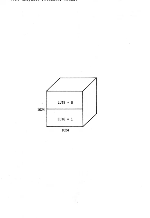
display information is supplied on LUT bank select O. Refer to
figure 5.1 for an illustration of this configuration.
SYSMOlJl:. 10 occurs only with two Mbytes. In this mode the CPU and
display banks occupy the same locations, with up to four banks
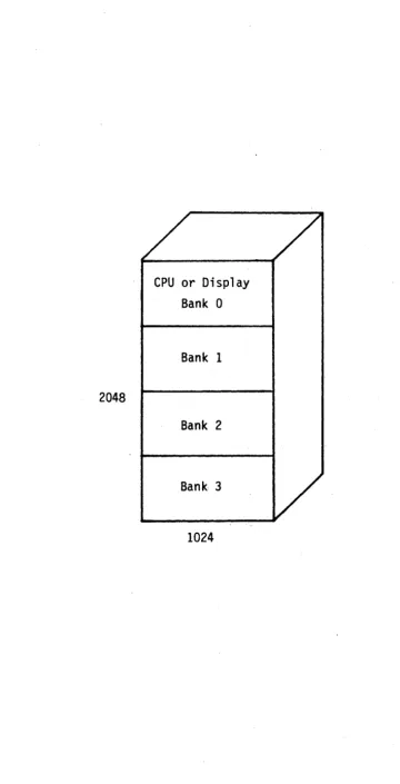
allowed. Re1,er to figure 5.2 for more information. Access all
addresses in any bank in this mode with no further hardware modifications.
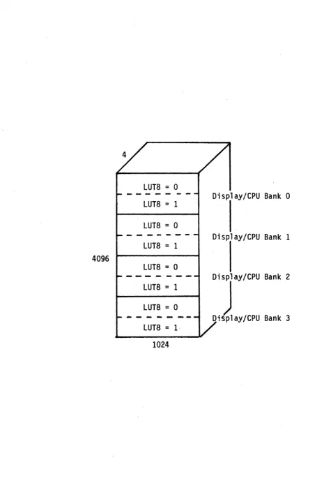
SYSMODE 11 allows either a 4-bit or 8-bit pixel. Bit 1 of
hardware register HREGI specifies the pixel depth. Bit 1 equal
to 0 flags the mode as IK x IK x 4. Bit 1 equal to 1 specifies
the mode as lK x lK x 8. The IK x lK x 4 mode mimics the
organization of SYSMODE 01 but with potentially four CPU and
display banks. In this configuration, the CPU and display banks
are identical. Refer to figure 5.3 for this configuration.
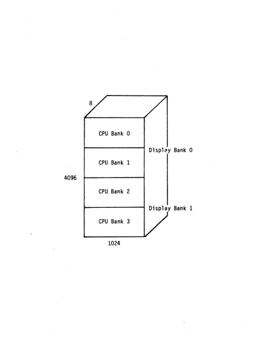
In the IK x lK x 8 mode, the references for the CPU and display
banks differ. Display bank 0 comprises CPU banks 0 and 1, while
display bank 1 holds CPU banks 2 and 3. Refer to figure 5.4.
VM-8851 Graphics Processor M.anual
LUTa
=
0
1024
1 - - - 1LUTa
=
1
[image:33.620.42.534.37.752.2]1024
VM-8851 Graphics Processor Manual
Figure 5.2
2048
CPU
or Display
Bank 0
Bank 1
Bank 2
Bank 3
1024
[image:34.624.75.436.54.760.2]VM-8851 Graphics Processor Manual
LUTS
=
0
LUTS
=
1
LUTS
=
0
-
-
-,_
...
--LUTS
=
1
4096
LUTS
=
0
---LUTS
=
1
LUTS
=
0
~---LUTS
=
1
1024
Display/CPU Bank 0
Display/CPU Bank 1
Display/CPU Bank 2
o;J,aY/CPU Bank 3
[image:35.627.37.513.46.736.2]VM-8851 Graphics Processor Manual
CPU Bank 0
Displ~y
Bank 0
CPU Bank 1
4096
CPU Bank 2
Display Bank 1
CPU
Bank 3
1024
[image:36.618.56.573.56.737.2]VM-88S1 Graphics Processor Manual
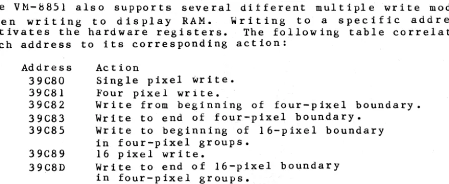
The VM-b851 also supports several different mUltiple write modes
when writing to display RAM. Writing to a specific address
activates the hardware registers. The following table correlates
each address to its corresponding action:
Action
Single pixel write. Four pixel write. Address
39C80 39C81 39C82 39C83 39C85
Write from beginning of four-pixel boundary. Write to end of four-pixel boundary.
Write to beginning of 16-pixel boundary
39C89 39C8D
in four-pixel groups. 16 pixel write.
Write to end of 16-pixel boundary in four-pixel groups.
Note that multiple pixel writes do not acknowledge the four
bit-plane mode. Therefore, to write in these modes, set the nibble
mask appropriately as described below.
The VM-b851 has the ability to mask out nibbles of the byte written to display RAM. bits in the hardware location NMBSLL.
5.6 - LUT Programming
one or both of the Set the nibble mask
The VM-8851 contains four banks of 256 word LUTs. LUT bank appears as
An entry in a
I
xI BIG I
R
I
where red (R) and green (G) reside in the bit whose least address
bit equals zero. To access the LUTs, assert CPU BLANK by
clearing the CPU BLANKL bit in HREG2. The LUT8 and L89 bits in
HREG1 control the bank selects of the LUTs. For all SYSMODEs.
except those with four pixel planes, LS9 is the high order bit and LUT8 is the low order bit for the LUT bank select.
5.7 - Interrupt Structure
The 8088 CPU has lines available as signal interrupts (INTR and
NMI). On the VM-8851, the interrupt controller, U4, f i l t e r s up
to seven level-sensitive interrupts on IRO to IR4, SINT, and
PBINT1, placing the appropriate vector on the bus. All seven
interrupts can be enabled or disabled by setting or clearing the
CPUIF flag. The interrupt controller drives lines DO to D7. The
interrupt table is located between OOOOH and 03FFH in the CPU
local memory. Line D7 always remains high, while lines DO-D6
[image:37.626.66.513.68.251.2]VM-8851 Gra~hics Processor Manual
represent the seven interrupts. The CPU will fetch the interrupt
vector from the 512-byte contiguous block in the upper half of
the interrupt table. The 5 1 2 - b y t e b I 0 c k m u s t contain the seven
4-byte interrupt vectors for IRO to IR4, SINT, and PBINT1. Place
the 4-byte pointer to the NMI service routine at location 0008R.
Refer to the Intel 8088 user's manual for more 8088 interrupt
handling details.