Databook
PRELIMINARY April 14, 1994
NexGen™
Microproducts, Inc. 1623 Buckeye DriveMilpitas, CA 95035
design. Wherever product internals are discussed, the information should be construed as conceptual in nature. No presumptions should be made about the internal design based on this document. Information about the internal design of NexGen products is provided via nondisclosure agreement ("NDA") on a need to know basis.
The material in this document is for information only and is subject to change without notice. NexGen reserves the right to make changes in the product specification and design without reservation and without notice to its users. THIS DOCUMENT DOES NOT CONSTITUTE A WARRANTY OF ANY KIND WITH RESPECT TO THE NEXGEN INC. PRODUCTS, AND NEXGEN INC. SHALL NOT BE LIABLE FOR ANY ERRORS THAT APPEAR IN THIS DOCUMENT.
All purchases of NexGen products shall be subject to NexGen's standard terms and conditions of sale. THE WARRANTIES AND REMEDIES EXPRESSLY SET FORTH IN SUCH TERMS AND CONDITIONS SHALL BE THE SOLE WARRANTIES AND THE BUYER'S SOLE AND EXCLUSIVE REMEDIES, AND NEXGEN INC. SPECIFICALLY DISCLAIMS ANY AND ALL OTHER WARRANTIES, WHETHER EXPRESS, IMPLIED OR STATUTORY, INCLUDING THE IMPLIED WARRANTIES OF FITNESS FOR A PARTICULAR PURPOSE, AGAINST INFRINGEMENT AND OF MERCHANTABILITY. No person is authorized to make any other warranty or representation concerning the performance of the NexGen products. In particular, NexGen's products are not specifically designed, manufactured or intended for sale as components for the planning, design, construction, maintenance, operation or use of any nuclear facility or other ultra-hazardous activity, and neither NexGen nor its suppliers shall have any liability with respect to such use
Trademark Acknowledgments
NexGen, Nx586, Nx587, RISC86, NexBus, NxPCI, and NxVL are trademarks of NexGen Microproducts, Inc ..
IBM, AT, and PS/2 are registered trademarks of International Business Machines, Inc. Intel is a registered trademark of Intel Corporation. i386, i387, i486 and Pentium are trademarks of Intel Corporation. Tri-state is a registered trademark of National Semiconductor Corporation. VL-Bus is a trademark of Video Electronics Standards Association.
Restricted Rights and Limitations
Contents
Preface ... v
Notation ... v
Related Publications ... vii
Nx586 Features and Signals ... 1
Nx586 Pinouts by Signal Names ... 4
Nx586 Pinouts by Pin Numbers ... 6
Nx586 NexBus Signals ... 10
NexBus Arbitration ... 10
NexBus Cycle Control ... 12
NexBus Cache Control. ... 14
NexBus Transceivers ... 16
NexBus Address and Data ... 17
Nx586 L2 Cache Signals ... 22
Floating Point-Coprocessor Bus Signals (on Nx586) ... 23
Nx586 System Signals ... 26
Nx586 Clock ... 26
Nx586 Interrupts and Reset ... 27
Nx586 Test and Reserved Signals ... 28
Nx586 Alphabetical Signal Summary ... '" ... 29
Nx587 Features and Signals ... 33
Nx587 Pinouts by Signal Names ... 35
Nx587 Pinouts by Pin Numbers ... 36
Floating Point Coprocessor Bus Signals (on Nx587) ... 39
Nx587 System Signals ... 41
Nx587 Clock ... ; ... 41
Nx587 Interrupts and Reset ... 42
Nx587 Test and Reserved Signals ... 42
Nx587 Alphabetical Signal Summary ... .43
Hardware Architecture •...•...•.•...•...•...•. 45
Bus Structure ... 45
NexBus ... 45
L2 Cache Bus ... 48
Floating-Point Coprocessor Bus ... 48
Operating Frequencies ... 49
Internal Architecture ... 51
Storage Hierarchy ... 52
Transaction Ordering ... 56
Cache and Memory Subsystem ... 57
Characteristics ... 57
Cache Coherency ... 59
State Transitions ... o . . . o . . . 60
Invalid State ... 0 . . . 0 . . . 63
Shared State ... 64
Exclusive State ... D . . . O . 0 . . . 64
Modified State ... 65
Interrupts ... 66
Clock Generation ... 67
Bus Operations ...•.•.•...•...•. 69
Accesses on the Level-2 Cache Bus ... 69
NexBus Arbitration and Address Phase ... 70
Single-Qword Memory Operations ... 71
Cache Line Memory Operations ... 0 . . . 76
110 Operations ... 76
Interrupt-Acknowledge Sequence ... 77
Halt and Shutdown Operations ... 78
Obtaining Exclusive Use Of Cache Blocks ... 79
Intervenor Operations ... 0 . . . 80
Modified Cache-Block Hit During Single-Qword Operations ... 81
Modified Cache-Block Hit During Four-Qword (Block) Operations. 82 Electrical Data ...•.•....•...•..•... 83
Mechanical Data ...•...•....•...•...•...•. 85
Glossary •..•...•...•.•..•...•....•...•...•...•... 93
PRELIMINARY
Figures
Figure 1 Figure 2 Figure 3 Figure 4 Figure 5 Figure 6 Figure 7 Figure 8 Figure 9 Figure 10 Figure 11 Figure 12 Figure 13 Figure 14 Figure 15 Figure 16 Figure 17 Figure 18 Figure 19 Figure 20 Figure 21 Figure 22 Figure 23 Figure 24 Figure 25 Figure 26 Figure 27 Figure 28 Figure 29 Figure 30 Figure 31 Figure 32 Figure 33Nx586 Signal Organization ... :3
Nx586 Pin List, By Signal Name ... .4
Nx586 Pin List, By Signal Name (continued) ... 5
Nx586 Pin List, By Pin Name (continued) ... 6
Nx586 Pin List, By Pin Number (continued) ... 7
Nx586 Pinout Diagram (Top View) ... 8
Nx586 Pinout Diagram (Bottom View) ... 9
NexBus Address and Status Phase ... 17
Byte-Enable Usage during 110 Transfers ... 19
Byte-Enable Usage during Memory Transfers ... 19
Bus-Cycle Types ... 20
Nx587 Signal Organization ... 34
Nx587 Pin List, By Signal Name ... 35
Nx587 Pin List, By Pin Number ... 36
Nx587 Pinout Diagram (Top View) ... 37
Nx587 Pinout Diagram (Bottom View) ... 38
Single-Processor System Diagram ... 46
Nx VL-Based Single-Processor System Diagram ... 47
Operating Frequencies (66MHz Processor) ... 50
Nx586 Internal Architecture ... 52
Storage Hierarchy (Reads) ... 54
Storage Hierarchy (Writes) ... 55
Cache Characteristics ... 57
Basic Cache-State Transitions ... 61
Cache State Controls ... 62
Bus Snooping ... 63
Clocking Modes ... 67
Level-2 Cache Read and Write ... 70
Fastest Single-Qword Read ... 72
Fast Single-Qword Read with a delayed GXACK ... 73
Single-Qword Read With Wait States using a delayed GXACK 74 Single-Qword Read With Wait States using GXHLD only ... 74
Fastest Single-Qword Write ... 75
Figure 34 Figure 35 Figure 36 Figure 37 Figure 38 Figure 39 Figure 39 Figure 40 Figure 41 Figure 42
Single-Qword Write With Wait States ... 76
Interrupt-Acknowledge Cycle ... 78
Halt and Shutdown Encoding ... 78
Single-Qword Read Hits Modified Cache Block ... 82
Nx586 Package Diagram (top) ... 86
Nx586 Package Diagram (side) ... 87
Nx586 Package Diagram (bottom) ... 88
Nx587 Package Diagram (top) ... 89
Nx587 Package Diagram (side) ... 90
PRELIMINARY
Preface
This databook covers two products: the Nx586™ processor (called the
processor), and the Nx587™ floating-point coprocessor. The databook is
written for system designers considering the use of these devices in their designs. We assume an experienced audience, familiar not only with system design conventions but also with the x86 architecture. The Glossary at the end of the book defines N exGen' s terminology, and the Index gives quick access to the subject matter.
NexGen's Applications Engineering Department welcomes your questions and will be glad to provide assistance. In particular, they can recommend system parts that have been tested and proven to work with NexGen™ products.
Notation
The following notation and conventions are used in this book:
Devices and Bus Names
•
•
•
Processor or CPU-The Nx586 processor described in this book.
Floating Point Coprocessor-The Nx587 floating-point coprocessor
described in this book.
NxVLTM Systems Logic-The NxVL system controller described in the
NxVL System Controller Databook.
•
NexBus™ System Bus-The Nx586 processor bus, including itsmultiplexed address/status and data bus (NxAD<63:0» and related control signals.
Signals and Timing Diagrams
•
Active-Low Signals-Signal names that are followed by an asterisk, such as ALE*, indicate active-low signals. They are said to be "asserted" or "active" in their low-voltage state and "negated" or "inactive" in their high-voltage state.Nx586lM
and Nx587lM
•
•
•
•
•
Bus Signals-In signal names, the notation <n:m> represents bits n through m of a bus.
Reserved Bits and Signals-Signals or bus bits marked "reserved" must be driven inactive or left unconnected, as indicated in the signal descriptions. These bits and signals are reserved by NexGen for future implementations. When software reads registers with reserved bits, the reserved bits must be masked. When software writes such registers, it must first read the register and change only the non-reserved bits before writing back to the register.
Source-In timing diagrams, the left-hand column indicates the "Source" of each signal. This is the chip or logic that outputs the signal. When signals are driven by multiple sources, all sources are shown, in the order in which they drive the signal. In some cases, signals take on different names as outputs are logically ORed in group-signal logic. In these cases, the signal source is shown with a subscript, where the subscript indicates the device or logic that originally caused the change in the signal.
Tri-state®-In timing diagrams, signal ranges that are high impedance are shown as a straight horizontal line half-way between the high and low level.
Invalid and Don't Care-In timing diagrams, signal ranges that are invalid or don't care are filled with a screen pattern.
Data
•
•
•
•
Quantities-A word is two bytes (16 bits), a dword or doubleword is four bytes (32 bits), and a qword or quadword is eight bytes (64 bits).
Addressing-Memory is addressed as a series of bytes on eight-byte (64-bit) boundaries, in which each byte can be separately enabled.
Abbreviations-The following notation is used for bits and bytes: Bits b as in "64b/qword"
Bytes B
kilo k
as in "32B/block"
as in "4kB/page"
Mega M as in "1Mb/sec"
Giga G as in "4GB of memory space"
Little Endian Convention-The byte with the address xx ... xxOO is in the least-significant byte position (little end). In byte diagrams, bit positions are numbered from right to left: the little end is on the right and the big end is on the left. Data structure diagrams in memory show small
PRELIMINARY
•
•
•
Bit Ranges-In a range of bits, the highest and lowest bit numbers are
separated by a colon, as in <63:0>.
Bit Values-Bits can either be set to 1 or cleared to O.
Hexadecimal and Binary Numbers-Unless the context makes
interpretation clear, hexadecimal numbers are followed by an h, binary numbers are followed by a b, and decimal numbers are followed by a d.
Related Publications
The following books treat various aspects of computer architecture, hardware design, and programming that may be useful for your understanding of NexGen products:
NexGen Products
•
NxVL System Controller Databook, NexGen, Milpitas, CA,Tel: (408) 435-0202.
x86 Architecture
•
John Crawford and Patrick Gelsinger, Programming the 80386, Sybex, San Francisco, 1987.Rakesh Agarwal, 80x86 Architecture & Programming, Volumes I and IT,
Prentice-Hall, Englewood Cliffs, NJ, 1991.
General References
•
John L. Hennessy and David A. Patterson, Computer Architecture, Morgan Kaufmann Publishers, San Mateo, CA, 1990.PRELIMINARY
Nx586 Features and Signals
The NexGen Nx586 processor is an advanced 5th generation 32-bit Superscalar x86 compatible processor that provides market leading performance. The Nx586 along with the Nx587 floating-point coprocessor are the core building blocks of a new class of personal computers. The following are some of the key features of the Nx586 Processor:
• Full x86 Binary Compatibility-Supports 8, 16 and 32-bit data types and operates in real, virtual 8086 and protected modes.
• Patented RISC86™ Superscalar Microarchitecture-Multiple operations are executed simultaneously during each cycle.
• Multi-Level Storage Hierarchy-Branch prediction, readable write queue, on-chip Ll code and data caches and unified L2 cache.
• Separate on-chip Ll Code and Data Caches-supports on-chip 4-way, 16kByte Code and 16kByte Data caches using MESI Cache Consistency Protocol.
•
•
•
•
•
•
•
•
On-Chip L2 Cache Controller- supporting 4-way, unified, MESI modified write-back cache coherency protocol on 256kB or 1MB of external cache using standard asynchronous SRAMs.
Patented Branch Prediction Logic-Reduces both control dependencies and branch cycle counts.
Dual-Port Caches-64-bit reads and writes are serviced in parallel in a single clock cycle.
Caches Decoupled From Processor Bus-Both the L 1 and L2 caches are accessed on separate dedicated buses.
Two-Phase, Non-Overlapped Clocking-Integrated phase-locked loop bus-clock doubler. Processor operates at twice the system bus frequency.
Three 64-Bit Synchronous Buses-NexBus (the processor bus), L2 SRAM bus, and Nx587 Floating-Point Coprocessor bus and is fully integrat3d into the processor microarchitecture.
Optional in Line Floating-Point Coprocessor- Nx587 operates in parallel with the Nx586 pipeline.
Advanced State-of-the-Art Fabrication Process-0.5 micron CMOS
Figure 1 shows the signal organization for the Nx586 processor. The processor supports signals for the NexBus (the processor bus), L2 cache, and the optional Nx587 Floating-Point Coprocessor. Many types of devices can be interfaced to the NexBus, including a backplane, multiple Nx586 processors, shared memory subsystems, high-speed 110, and industry-standard buses. All signals are synchronous to the NexBus clock (CLK) and transition at the rising edge of the clock with the exception of four asynchronous signals: INTR *, NMI*, GATEA20, and SLOTID<3:0>. All bi-directional NexBus signals are floated unless they are needed during specific time periods, as specified in the Bus Operation chapter. The normal state for all reserved bits is high.
Two types of NexBus signals deserve special mention:
•
•
Group Signals-There are several group signals on the NexBus, typically denoted by signal names beginning with the letter "G." Active-low signals such as ALE* are driven by each NexBus device, and the arbiter derives an active-high group signal (such as GALE) and distributes it back to each device. When the Nx VL is used, these group signals are generated within the NxVL.
Processor Bu (NexBus) Arbitration Cycle Control Cache Control Tranceiver Control Address/Data s ~ A ~ 10 6/ /
7/
"-6/ /
3/
/
~
64
\
/
[image:14.615.110.538.108.664.2]v
Figure 1 Nx586 Signal Organization
I L2 Cache Cache Control Cache Bank I Address Data
f
L~"
~
2 15[/' 64
"""'---.---?- Nx587 F Coproc essor loating-Point
~ Nx586 Processor A
II
1\
~l
r- ~v 10/ 6 / 11
,.. 16/ 7 5/ / 6/ / 4/ / 5/ / 64 ~
.
-h v Micro-Operations Control Tag Status Arbitration Tag Data ! ISystem and Test
L -_ _ _ _ _ Test L
_ _ _ _ _ _ _ _ _ Interrupt and Reset
. Clock
Mode and Chip Select
007
Nx586 Pinouts
by
Signal Names
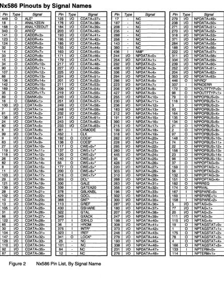
Pin Type Signal Pin Type Signal Pin Type Signal Pin Type Signal
[image:15.615.76.522.121.679.2]Pin Type Signal Pin Type Signal Pin Type Signal Pin Type Signal 355 I NPWREQ 457 I/O NxAD<55> 146 VCC4 54 VSS 319 I NPWVAL 329 I/O NxAD<56> 157 VCC4 75 VSS 321 0 NREQ* 328 I/O NxAD<57> 162 VCC4 91 VSS 296 I/O NxAD<O> 365 I/O NxAD<58> 173 VCC4 112 VSS 267 I/O NxAD<1> 439 I/O NxAD<59> 178 VCC4 128 VSS 307 I/O NxAD<2> 364 I/O NxAD<60> 189 VCC4 149 VSS 297 I/O NxAD<3> 456 I/O NxAD<61> 194 VCC4 154 VSS 443 I/O NxAD<4> 363 I/O NxAD<62> 205 VCC4 165 VSS
444 I/O NxAD<5> 381 I/O NxAD<63> 210 VCC4 170 VSS 463 I/O NxAD<6> 73 0 NxADINUSE 221 VCC4 181 VSS 312 I/O NxAD<7> 447 I OWNABL 226 VCC4 186 VSS 313 I/O NxAD<8> 76 I P4REF 237 VCC4 197 VSS 315 I/O NxAD<9> 453 I PHE1 242 VCC4 202 VSS 281 I/O NxAD<10> 379 I PHE2 253 VCC4 213 VSS 283 I/O NxAD<11> 153 I POPHOLD 258 VCC4 218 VSS 459 I/O NxAD<12> 160 I PULLHIGH 269 VCC4 229 VSS 460 I/O NxAD<13> 145 I PULLHIGH 274 VCC4 234 VSS 441 I/O NxAD<14> 320 I/O PULLHIGH 285 VCC4 245 VSS 348 I/O NxAD<15> 357 I/O PULLHIGH 290 VCC4 250 VSS 387 I/O NxAD<16> 376 I/O PULLHIGH 301 VCC4 261 VSS 370 I/O NxAD<17> 431 I/O PULLHIGH 306 VCC4 266 VSS 331 I/O NxAD<18> 432 I/O PULLHIGH 317 VCC4 277 VSS 333 I/O NxAD<19> 433 I/O PULLHIGH 332 VCC4 282 VSS 325 I/O NxAD<20> 450 I/O PULLHIGH 354 VCC4 293 VSS 345 I/O NxAD<21> 451 I/O PULLHIGH 369 VCC4 298 VSS 327 I/O NxAD<22> 264 I/O PULLLOW 391 VCC4 309 VSS 383 I/O NxAD<23> 272 I PTEST 392 VCC4 314 VSS 347 I/O NxAD<24> 214 I RESET* 393 VCC4 335 VSS 384 I/O NxAD<25> 362 I RESETCPU* 394 VCC4 351 VSS 458 I/O NxAD<26> 144 I SERIALIN 395 VCC4 372 VSS 346 I/O NxAD<27> 280 0 SERIALOUT 396 VCC4 388 VSS 438 I/O NxAD<28> 448 0 SHARE* 397 VCC4 409 VSS 382 I/O NxAD<29> 130 I SLOTID<O> 398 VCC4 410 VSS 437 I/O NxAD<30> 161 I SLOTID<1> 399 VCC4 411 VSS 455 I/O NxAD<31> 152 I SLOTID<2> 400 VCC4 412 VSS 259 I/O NxAD<32> 127 I SLOTID<3> 401 VCC4 413 VSS 257 I/O NxAD<33> 374 I TESTPWR* 402 VCC4 414 VSS 265 I/O NxAD<34> 108 I TPH1 403 VCC4 415 VSS 275 I/O NxAD<35> 126 I TPH2 404 VCC4 416 VSS 273 I/O NxAD<36> 57 I VCC4 405 VCC4 417 VSS 462 I/O NxAD<37> 58 I VCC4 406 VCC4 418 VSS 304 I/O NxAD<38> 59 I VCC4 324 VDDA 419 VSS 426 I/O NxAD<39> 60 I VCC4 38 VSS 420 VSS 299 I/O NxAD<40> 61 I VCC4 39 VSS 421 VSS 289 I/O NxAD<41> 62 I VCC4 40 VSS 422 VSS 291 I/O NxAD<42> 63 I VCC4 41 VSS 423 VSS 305 I/O NxAD<43> 64 I VCC4 42 VSS 424 VSS 440 I/O NxAD<44> 65 I VCC4 43 VSS 425 VSS 366 I/O NxAD<45> 66 I VCC4 44 VSS 358 0 XACK* 367 I/O NxAD<46> 67 I VCC4 45 VSS 386 0 XBCKE* 385 I/O NxAD<47> 68 I VCC4 46 VSS 461 0 XBOE* 407 I/O NxAD<48> 69 I VCC4 47 VSS 454 0 XHLD* 389 I/O NxAD<49> 70 I VCC4 48 VSS 442 0 XNOE* 350 I/O NxAD<50> 71 I VCC4 49 VSS 360 0 XPH1 352 I/O NxAD<51> 72 I VCC4 50 VSS 342 0 XPH2 343 I/O NxAD<52> 94 I VCC4 51 VSS 434 0 XREF 344 I/O NxAD<53> 109 I VCC4 52 VSS 435 I XSEL 326 I/O NxAD<54> 131 I VCC4 53 VSS
Figure 3 Nx586 Pin List, By Signal Name (continued)
Nx586 Pinouts by Pin Numbers
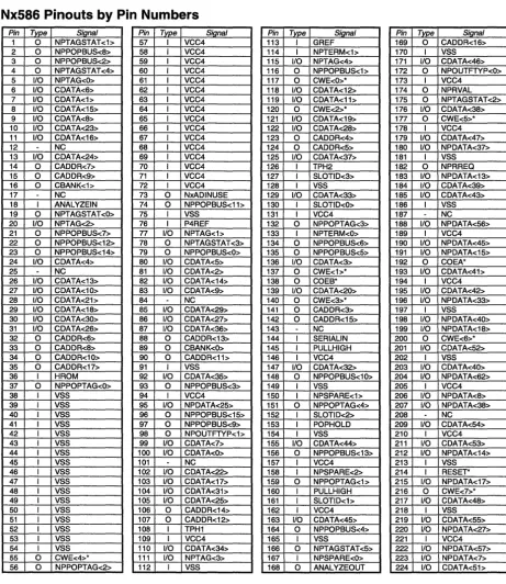
Pin Type Signal Pin Type Signal Pin Type Signal Pin Type Signal
1 0 NPTAGSTAT <1> 57 VCC4 113 I GREF 169 0 CADDR<16> 2 0 NPPOPBUS<8> 58 VCC4 114 I NPTERM<1> 170 I VSS 3 0 NPPOPBUS<2> 59 VCC4 115 I/O NPTAG<4> 171 1/0 CDATA<46> 4 0 NPTAGSTAT<4> 60 VCC4 116 0 NPPOPBUS<1 > 172 0 NPOUTFTYP<O> 5 I/O NPTAG<O> 61 VCC4 117 0 CWE<O>* 173 I VCC4
6 1/0 CDATA<6> 62 VCC4 118 1/0 CDATA<12> 174 0 NPRVAL 7 1/0 CDATA<1> 63 VCC4 119 1/0 CDATA<11> 175 0 NPTAGSTAT<2> 8 1/0 CDATA<15> 64 VCC4 120 0 CWE<2>* 176 1/0 CDATA<38> 9 1/0 CDATA<8> 65 VCC4 121 I/O CDATA<19> 177 0 CWE<5>* 10 1/0 CDATA<23> 66 VCC4 122 1/0 CDATA<28> 178 I VCC4 11 1/0 CDATA<16> 67 VCC4 123 0 CADDR<4> 179 1/0 CDATA<47> 12
-
NC 68 VCC4 124 0 CADDR<5> 180 1/0 NPDATA<37> 13 1/0 CDATA<24> 69 VCC4 125 1/0 CDATA<37> 181 I VSS 14 0 CADDR<7> 70 VCC4 126 I TPH2 182 0 NPRREQ 15 0 CADDR<9> 71 VCC4 127 I SLOTID<3> 183 I/O NPDATA<13> 16 0 CBANK<1> 72 VCC4 128 I VSS 184 I/O CDATA<39> 17-
NC 73 0 NxADINUSE 129 1/0 CDATA<33> 185 I/O CDATA<43> 18 I ANALYZEIN 74 0 NPPOPBUS<11> 130 I SLOTID<O> 186 I VSS 19 0 NPTAGSTAT <0> 75 I VSS 131 I VCC4 187 - NC20 1/0 NPTAG<2> 76 I P4REF 132 0 NPPOPTAG<3> 188 I/O NPDATA<56> 21 0 NPPOPBUS<7> 77 1/0 NPTAG<1> 133 I NPTERM<O> 189 I VCC4 22 0 NPPOPBUS<12> 78 0 NPTAGSTAT<3> 134 0 NPPOPBUS<6> 190 I/O NPDATA<45> 23 0 NPPOPBUS<14> 79 0 NPPOPBUS<O> 135 0 NPPOPBUS<5> 191 1/0 NPDATA<15> 24 1/0 CDATA<4> 80 1/0 CDATA<5> 136 1/0 CDATA<3> 192 0 COEA* 25
-
NC 81 1/0 CDATA<2> 137 0 CWE<1>* 193 1/0 CDATA<41> 26 1/0 CDATA<13> 82 1/0 CDATA<14> 138 0 COEB* 194 I VCC4 27 1/0 CDATA<10> 83 1/0 CDATA<9> 139 1/0 CDATA<20> 195 1/0 CDATA<42> 28 1/0 CDATA<21> 84-
NC 140 0 CWE<3>* 196 1/0 NPDATA<33> 29 1/0 CDATA<18> 85 I/O CDATA<29> 141 0 CADDR<3> 197 I VSS 30 1/0 CDATA<30> 86 1/0 CDATA<27> 142 0 CADDR<15> 198 1/0 NPDATA<40> 31 1/0 CDATA<26> 87 1/0 CDATA<36> 143 NC 199 1/0 NPDATA<18> 32 0 CADDR<6> 88 0 CADDR<13> 144 I SERIALIN 200 0 CWE<6>* 33 0 CADDR<8> 89 0 CBANK<O> 145 I PULLHIGH 201 1/0 CDATA<52> 34 0 CADDR<10> 90 0 CADDR<11> 146 I VCC4 202 I VSS 35 0 CADDR<17> 91 I VSS 147 1/0 CDATA<32> 203 I/O CDATA<40> 36 I HROM 92 1/0 CDATA<35> 148 0 NPPOPBUS<10> 204 1/0 NPDATA<62> 37 0 NPPOPTAG<O> 93 0 NPPOPBUS<3> 149 I VSS 205 I VCC4 38 I VSS 94 I VCC4 150 I NPSPARE<1> 206 1/0 NPDATA<8> 39 I VSS 95 1/0 NPDATA<25> 151 0 NPPOPTAG<4> 207 1/0 NPDATA<38> 40 I VSS 96 0 NPPOPBUS<15> 152 I SLOTID<2> 208-
NC41 I VSS 97 0 NPPOPBUS<9> 153 I POPHOLD 209 1/0 CDATA<54> 42 I VSS 98 0 NPOUTFTYP<1> 154 I VSS 210 I VCC4 43 VSS 99 1/0 CDATA<7> 155 1/0 CDATA<44> 211 1/0 CDATA<53> 44 VSS 100 1/0 CDATA<O> 156 0 NPPOPBUS<13> 212 1/0 NPDATA<14>
45 VSS 101
-
NC 157 I VCC4 213 I VSS46 VSS 102 1/0 CDATA<22> 158 I NPSPARE<2> 214 I RESET* 47 VSS 103 1/0 CDATA<17> 159 0 NPPOPTAG<1> 215 1/0 NPDATA<17> 48 VSS 104 1/0 CDATA<31> 160 I PULLHIGH 216 0 CWE<7>* 49 VSS 105 1/0 CDATA<25> 161 I SLOTID<1> 217 1/0 CDATA<48> 50 VSS 106 0 CADDR<14> 162 I VCC4 218 I VSS 51 VSS 107 0 CADDR<12> 163 1/0 CDATA<45> 219 1/0 CDATA<55> 52 VSS 108 I TPH1 164 0 NPPOPBUS<4> 220 1/0 NPDATA<27>
53 VSS 109 I VCC4 165 I VSS 221 I VCC4
[image:17.618.64.526.119.651.2]Pin Type Signal Pin Type Signal Pin Type Signal Pin Type Signal
[image:18.617.92.546.121.635.2]225 1/0 CDATA<50> 285 I VCC4 345 1/0 NxAD<21> 405 I VCC4 226 I VCC4 286 1/0 NPDATA<6> 346 1/0 NxAD<27> 406 I VCC4 227 1/0 CDATA<49> 287 1/0 NPDATA<36> 347 1/0 NxAD<24> 407 1/0 NxAD<48> 228 1/0 NPDATA<21> 288 - NC 348 1/0 NxAD<15> 408 1/0 NPDATA<3> 229 I VSS 289 I/O NxAD<41> 349 I GXACK 409 VSS 230 1/0 NPDATA<11> 290 I VCC4 350 1/0 NxAD<50> 410 VSS 231 1/0 NPDATA<47> 291 1/0 NxAD<42> 351 I VSS 411 VSS 232 1/0 CDATA<60> 292 1/0 NPDATA<2> 352 1/0 NxAD<51> 412 VSS 233 1/0 CDATA<63> 293 I VSS 353 1/0 NPDATA<63> 413 VSS 234 I VSS 294 1/0 NPDATA<5> 354 I VCC4 414 VSS 235
-
NC 295 1/0 NPDATA<22> 355 I NPWREQ 415 VSS 236 1/0 NPDATA<12> 296 1/0 NxAD<O> 356 1/0 NPDATA<32> 416 VSS 237 I VCC4 297 1/0 NxAD<3> 357 1/0 PULLHIGH 417 VSS 238 1/0 NPDATA<50> 298 I VSS 358 0 XACK* 418 VSS 239 1/0 NPDATA<60> 299 1/0 NxAD<40> 359 0 DCL* 419 VSS 240 1/0 CDATA<56> 300 1/0 NPDATA<35> 360 0 XPH1 420 VSS 241 1/0 CDATA<61> 301 I VCC4 361 I CKMODE 421 VSS 242 I VCC4 302 1/0 NPDATA<34> 362 I RESETCPU* 422 VSS 243 1/0 CDATA<62> 303 1/0 NPDATA<28> 363 1/0 NxAD<62> 423 VSS 244 1/0 NPDATA<O> 304 1/0 NxAD<38> 364 1/0 NxAD<60> 424 VSS 245 I VSS 305 1/0 NxAD<43> 365 1/0 NxAD<58> 425 I VSS 246 1/0 NPDATA<43> 306 I VCC4 366 1/0 NxAD<45> 426 1/0 NxAD<39> 247 1/0 NPDATA<39> 307 1/0 NxAD<2> 367 1/0 NxAD<46> 427 1/0 NPDATA<9> 248 1/0 CDATA<59> 308 1/0 NPDATA<41> 368 I GNT* 428 1/0 NPDATA<26> 249 1/0 CDATA<58> 309 I VSS 369 I VCC4 429 I GDCl 250 I VSS 310 I/O NPDATA<29> 370 1/0 NxAD<17> 430 I GSHARE 251 1/0 CDATA<57> 311 1/0 NPDATA<58> 371 1/0 NPDATA<54> 431 1/0 PUlLHIGH 252 1/0 NPDATA<61> 312 1/0 NxAD<7> 372 I VSS 432 1/0 PULLHIGH 253 I VCC4 313 1/0 NxAD<8> 373 1/0 NPDATA<42> 433 1/0 PULLHIGH 254 1/0 NPDATA<1> 314 I VSS 374 I TESTPWR* 434 0 XREF 255 1/0 NPDATA<10> 315 1/0 NxAD<9> 375 I INTR* 435 I XSEL 256-
NC 316 1/0 NPDATA<53> 376 1/0 PUllHIGH 436 I NMI* 257 1/0 NxAD<33> 317 I VCC4 377 I GXHlD 437 1/0 NxAD<30> 258 I VCC4 318 1/0 NPDATA<19> 378 I GBLKNBl 438 1/0 NxAD<28> 259 1/0 NxAD<32> 319 I NPWVAL 379 I PHE2 439 1/0 NxAD<59> 260 1/0 NPDATA<23> 320 1/0 PULLHIGH 380-
NC 440 1/0 NxAD<44> 261 I VSS 321 0 NREQ* 381 1/0 NxAD<63> 441 1/0 NxAD<14> 262 1/0 NPDATA<20> 322 I GTAL 382 1/0 NxAD<29> 442 0 XNOE* 263 1/0 NPDATA<31> 323 I IREF 383 I/O NxAD<23> 443 1/0 NxAD<4> 264 1/0 PULLLOW 324 I VDDA 384 1/0 NxAD<25> 444 1/0 NxAD<5> 265 1/0 NxAD<34> 325 1/0 NxAD<20> 385 1/0 NxAD<47> 445 1/0 NPDATA<24> 266 I VSS 326 1/0 NxAD<54> 386 0 XBCKE* 446 0 NPIRQ* 267 1/0 NxAD<1> 327 1/0 NxAD<22> 387 I/O NxAD<16> 447 I OWNABL 268 1/0 NPDATA<30> 328 1/0 NxAD<57> 388 I VSS 448 0 SHARE* 269 I VCC4 329 1/0 NxAD<56> 389 1/0 NxAD<49> 449 0 AlE* 270 1/0 NPDATA<52> 330 I GALE 390 1/0 NPDATA<16> 450 1/0 PUllHIGH 271 1/0 NPDATA<51> 331 1/0 NxAD<18> 391 VCC4 451 1/0 PULLHIGH 272 I PTEST 332 I VCC4 392 VCC4 452 I ClK 273 1/0 NxAD<36> 333 1/0 NxAD<19> 393 VCC4 453 I PHE1 274 I VCC4 334 1/0 NPDATA<59> 394 VCC4 454 0 XHLD* 275 1/0 NxAD<35> 335 I VSS 395 VCC4 455 1/0 NxAD<31> 276 1/0 NPDATA<48> 336 1/0 NPDATA<4> 396 VCC4 456 1/0 NxAD<61> 277 I VSS 337 I NPNOERR 397 VCC4 457 1/0 NxAD<55> 278 1/0 NPDATA<44> 338 1/0 NPDATA<46> 398 VCC4 458 1/0 NxAD<26> 279 1/0 NPDATA<49> 339 I GATEA20 399 VCC4 459 1/0 NxAD<12> 280 0 SERIALOUT 340 0 AREQ* 400 VCC4 460 1/0 NxAD<13> 281 1/0 NxAD<10> 341 0 LOCK* 401 VCC4 461 0 XBOE* 282 I VSS 342 0 XPH2 402 VCC4 462 1/0 NxAD<37> 283 1/0 NxAD<11> 343 1/0 NxAD<52> 403 VCC4 463 1/0 NxAD<6> 284 1/0 NPDATA<55> 344 1/0 NxAD<53> 404 VCC4Figure 5 Nx586 Pin List, By Pin Number (continued)
068
069
Figure 7 Nx586 Pinout Diagram (Bottom View)
Nx586 NexBus Signals
Note: The resistor value required for all signals to be pulled up or down should be in the range between lkO and 5kQ. The pull up resistor must be connected to the V CC (4V) plane.
NexBus Arbitration
,/ NREQ* 0 NexBus Request-Asserted by the processor to the NexBus Arbiter to secure control of the NexBus. This signal remains active until one CLK period after GALE* is received from the NexBus Arbiter. During speculative reads, the Nx586 may deactivate NREQ* before GNT* is received if the transfer is no longer needed. In systems using the Nx VL as the NexBus Arbiter, NREQ* is treated the same as AREQ*; when the NexBus control is granted, control of all other buses is also granted at the same time.
If the processor does not know which bus its intended resource is on, it asserts NREQ*. If a GT AL is subsequently returned, the processor assumes the resources are on another system bus and it retries the transfer by asserting AREQ* .
./ AREQ* 0 Alternate-Bus Request-Asserted by the processor to the NexBus Arbiter to secure control of the NexBus and any other buses (called alternate buses) supported by the system. This signal remains active until GNT* is received from the NexBus Arbiter; unlike NREQ*, the processor does not make speculative requests with AREQ*. The NexBus Arbiter does not issue GNT* until the other system buses are available.
In systems using the Nx VL as the NexBus Arbiter (shown in Figure 18), AREQ* and NREQ* have the same effect: either one causes the Nx VL global bus arbiter to grant all buses to the winning requester at the end of the current bus cycle.
J GNT* I Grant NexBus-Asserted by the NexBus Arbiter to indicate
LOCK*
o
SLOTID<3:0> I
PRELIMINARY
Bus Lock-Asserted by the processor to the NexBus Arbiter when multiple bus operations should be performed sequentially and uninterruptedly. This signal is used by the NexBus Arbiter to determine the end of a bus sequence. Cache-block fills are not locked; they are implicitly treated as atomic reads. Some NexBus Arbiters (but not the NxVL) may allow masters on system buses other than NexBus (Le., on an alternate bus) to intervene in a locked NexBus transaction. To avoid this, the processor must assert AREQ* .
LOCK* is typically software configured to be asserted for read-modify-writes and explicitly locked instructions.
NexBus Slot ID-These bits identify NexBus backplane slots. SLOTID 1111 (OFh) is reserved for the system's primary processor. Normally, only the primary processor receives PC-compatible signals such as RESET* , RESETCPU*, INTR *, NMI*, and GA TEA20, and this processor is responsible for initializing any secondary processors. SLOTID 0000 is reserved for the system logic that interfaces the NexBus to any other system buses (called the alternate-bus inteiface). The Nx VL acts as an Altemate-Bus Interface. This signal is asynchronous to the NexAltemate-Bus clock.
Nx586Thl and Nx587Thl
NexBus Cycle Control
/ ALE*
o
GALE I
GTAL I
XACK*
o
Address Latch Enable-Asserted by the processor to backplane logic or to the system-logic interface between the NexBus and any other system buses (called the alternate-bus
inteiface) when the processor is driving valid address and
status information on the NxAD<63:0> bus.
Group Address Latch Enable-Asserted by a backplane NAND of all ALE* signals, to indicate that the NexBus address and status can be latched. Systems using the Nx VL, GALE is generated by the NxVL.
Group Try Again Later-Asserted by the system-logic interface between the NexBus and other system buses (called the alternate-bus inteiface) to indicate that the attempted bus-crossing operation cannot be completed, because the system-logic bus interface is busy or cannot access the other system bus. In response, the processor aborts its current operation and attempts to re-try it by asserting AREQ*, thereby assuring that the processor will not receive a GNT* until the desired system bus is available.
A bus-crossing operation can happen without the system-logic bus interface asserting GT AL and without the processor asserting AREQ*, if the other system bus and its system-logic interface are both available when the processor asserts NREQ*. The GT AL and AREQ* protocol is only used when NREQ* is asserted. while either the other system bus or its system-logic interface is unavailable. The protocol prevents deadlocks and prevents the processor from staying on the NexBus until the other system bus becomes available.
Unlike other group signals, which are the logical OR of a set of active-low signals generated by each participating device in the group, GTAL does not have such a corresponding active-low signal.
GXACK I
XIll.D*
o
GXIll.D I
PRELIMINARY
Group Transfer Acknowledge-Asserted by a backplane NAND of all XACK* signals, to indicate that a NexBus device is prepared to respond as a slave to the processor's current operation. The system-logic interface between the NexBus and other system buses (called the alternate-bus
interface) monitors the XACK* responses from all adapters.
In systems using the NxVL as the Alternate-Bus Interface, when no XACK* response is forthcoming within three clocks, the Nx VL asserts GXACK and initiates a
bus-crossing operation. GXACK must be asserted for the
transaction to continue. In general, since the system-logic interface to other system buses may take a variable number of cycles to respond to a GALE, the maximum time between assertion of GALE and the responding assertion of GXACK is not specified.
Transfer Hold-Asserted by the processor, as slave or master, to backplane logic or to the system-logic interface between the NexBus and other system buses (called the
alternate-bus inteiface) in response to another NexBus
master's request for data, when the processor is unable to respond on the next clock after GXACK. In case the processor is the master, an inactive XIll..-D* indicates that the CPU is not ready to complete the transfer.
Group Transfer Hold-Asserted by a backplane NAND of all XHLD* signals, to indicate that a slave cannot respond to the processor's request. GXIll..-D causes wait states to be inserted into the current operation. Both the master and the slave must monitor GXIll..-D to synchronize data transfers.
During a bus-crossing read by the processor, the simultaneous assertion of GXACK and negation of GXIll..-D indicates that valid data is available on the bus. During a bus-crossing write, the same signal states indicate that data has been accepted by the slave.
Nx586lM
and Nx587lM
NexBus Cache Control
DCL* 0 Dirty Cache Line-During reads by another NexBus master, this signal is asserted by the processor to indicate that the location being accessed is cached by the processor's L2 cache in a modified (dirty) state.
The requesting master's cycle is then aborted so that the processor, as an intervenor, can preemptively gain control of the NexBus and write back its modified data to main memory. While the data is being written to memory, the requesting master reads it off the NexBus. The assertion of DCL * is the only way in which atomic 32-byte cache-block fills by another NexBus master can be preempted by the processor for the purpose of writing back dirty data.
During writes by another NexBus master, this signal is likewise asserted by the processor to indicate that it has a
modified copy of the data. But in this case, the initiating master is allowed to finish its write to memory. The NexBus Arbiter must then guarantee that the processor asserting DCL * gains access to the bus in the very next arbitration grant, so that the processor can write back all of its modified data except the bytes written by the initiating master. (In this case, the initiating master's data is more recent than the data cached by the processor asserting DCL * .)
GDCL I Group Dirty Cache Line-Asserted by a backplane NAND
of all DCL* signals, to indicate that a NexBus device has, in its cache, a modified copy of the data being accessed. During reads, when the processor is the bus master, the processor aborts its cycle so that the other caching device can write back its data; the processor reads the data on the fly. During writes, when the processor is the bus master, the processor finishes its write before the device asserting DCL * writes back all bytes other than those written by the processor.
OWNABL I
SHARE*
o
GSHARE I
PRELIMINARY
Ownable-Asserted by the system logic during accesses by the processor to locations that may be cached in the exclusive state. Negated during accesses that may only be cached in the shared state, such as bus-crossing accesses to an address space that cannot support the MESI cache-coherency protocol. All NexBus addresses are assumed to be cacheable in the exclusive state.
The OWNABL signal is provided in case the system logic needs to restrict caching to certain locations. In single-processor systems using the NxVL, that does not have an OWNABL signal and the processor's OWNABL input is typically tied high for write-back configurations to allow caching in the exclusive state on all reads.
Shared Data-Asserted by the processor during block reads by another NexBus master to indicate to the other master that its read hit in a block cached by the processor.
Group Shared Data-Asserted by a backplane NAND of all SHARE* signals, to indicate that the data being read must be cached in the shared state, if OWN* (NxAD<49> ) is negated. However, if GSHARE and OWN* are both negated during the read, the data may be promoted to the exclusive state, since no other NexBus device has declared via SHARE* that it has cached a copy. Instruction fetches are always shared.
NexBus Transceivers
XBCKE*
o
XBOE*
o
XNOE*
o
Transceiver NxAD-Bus Clock Enable-Asserted by the processor to clock registered transceivers and latch addresses and data from the NxAD<63:0> bus for subsequent driving onto the AD<63:0> bus (see Figure 18). There is no comparable clock-enable for the NexBus side of these transceivers; they are always enabled on the NexBus side.
In systems using the Nx VL as the interface to other system buses, these NexBus transceivers are emulated within the NxVL, and this signal is tied to the same-named input on the NxVL.
Transceiver-to-NxAD-Bus Output Enable-Asserted by the processor to enable the registered transceivers and drive addresses and data onto the NxAD<63:0> bus from the AD<63:0> bus (see Figure 19).
In systems using the Nx VL as the interface to other system buses, these transceivers are emulated within the Nx VL , and this signal is tied to the same-named input on the NxVL .
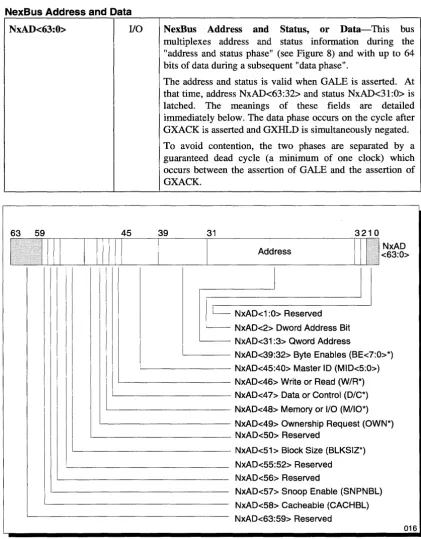
NexBus Address and Data NxAD<63:0> liD
63 59 45
I'
i1111 I 1111INexBus Address and Status, or Data-This bus multiplexes address and status information during the "address and status phase" (see Figure 8) and with up to 64 bits of data during a subsequent "data phase".
The address and status is valid when GALE is asserted. At that time, address NxAD<63:32> and status NxAD<31:0> is latched. The meanings of these fields are detailed immediately below. The data phase occurs on the cycle after GXACK is asserted and GXHLD is simultaneously negated.
To avoid contention, the two phases are separated by a guaranteed dead cycle (a minimum of one clock) which occurs between the assertion of GALE and the assertion of GXACK.
39 31 3210
Address
I
c=
NxAD<1 :0> Reserved ~ NxAD<2> Dword Address BitNxAD<31 :3> Qword Address
NxAD<39:32> Byte Enables (BE<7: 0>*) NxAD<45:40> Master ID (MID<5:0»
NxAD<46> Write or Read (W/R*) NxAD<47> Data or Control (D/C*)
NxAD<48> Memory or 1/0 (M/IO*)
NxAD<49> Ownership Request (0 WN*) NxAD<50> Reserved
NxAD<51> Block Size (BLKSIZ*)
NxAD<55:52> Reserved NxAD<56> Reserved
NxAD<57> Snoop Enable (SNPNBL
NxAD<58> Cacheable (CACHBL) NxAD<63.59> Reserved
[image:28.617.106.528.119.659.2]016
Figure 8 NexBus Address and Status Phase
NxAD<1:0>
address phase
NxAD<2>
address phase
NxAD<31:3>
address phase
NxAD<39:32>
address phase
110
110
110
110
Reserved-These bits must be driven high by the bus master.
ADRS<2> (Dword Address)-For 110 cycles, this bit selects between the four-byte doublewords (dwords) in an eight-byte quadword (qword). For memory cycles, the bit is driven but the information is not normally used.
ADRS<31:3> (Qword Address)-For memory cycles, these bits address an eight-byte quadword (qword) within the 4GB memory address space. For 110 cycles, NxAD<15:3> specifies a qword within the 64kB 110 address space and NxAD<3l:l6> are driven low by the processor. In either case, the addressed data may be further restricted by the BE<7:0>* bits on NxAD<39:32>. Memory cycles (but not 110 cycles) may be expanded to additional consecutive qwords by the BLKSIZ<l:O>* bits on NxAD<Sl:50>.
BE<7:0>* (Byte Enables)-Byte-enable bits for the data phase of the NxAD<63:0> bus. BE<O>* corresponds to the byte on NxAD<7:0>, and BE<7>* corresponds to the byte on NxAD<63:56>. The meaning of these bytes is shown in Figure 9 and 10.
Transfer Type Meaning of BE<7:0>
*
110 BE<3:0>* specify the bytes to transfer [image:30.618.114.525.130.534.2]on NxAD<31:0>. BE<7:4>* are driven high by the processor.
Figure 9 Byte-Enable Usage during I/O Transfers
Transfer Type Meaning of BE<7:0>
*
Memory Single Qword Read or BE<7:0>* specify the bytes to transfer Write on NxAD<63:0>.
Four-Qword Block Write BE<7 :0>* specify the bytes to transfer on NxAD<63:0> for first qword only. For all other qwords, BE<3:0>* are implicit zeros. and all bytes are transferred.
Four-Qword Block Read BE<7 :0>* specify the bytes that are to (Cache-Block Fill) be fetched immediately.
Figure 10 Byte-Enable Usage during Memory Transfers
NxAD<45:40> 110 MID<S:O> (Master ID)-These bits indicate to a slave, and
address phase to the system-logic interface between the NexBus and other system buses (called the alternate-bus inteiface) during
bus-crossing cycles, the identity of the NexBus master that initiated the cycle. The most-significant four bits are the device's SLOTID<3:0> bits. The least-significant two bits are the device's DEVICE<1:0> bits. In systems using the NxVL as the interface to other system buses, MID 000000 is reserved for the NxVL .
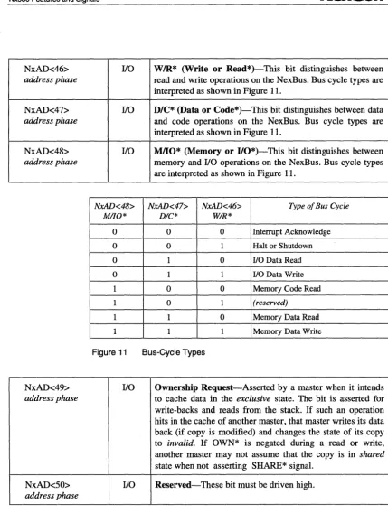
NxAD<46> liD WIR* (Write or Read*)-This bit distinguishes between
address phase read and write operations on the NexBus. Bus cycle types are interpreted as shown in Figure 11.
NxAD<47> liD D/C* (Data or Code*)-This bit distinguishes between data
address phase and code operations on the NexBus. Bus cycle types are interpreted as shown in Figure 11.
NxAD<48> liD M1I0* (Memory or 110*)-This bit distinguishes between
address phase memory and liD operations on the NexBus. Bus cycle types are interpreted as shown in Figure 11.
NxAD<4B> NxAD<47> NxAD<46> Type of Bus Cycle
MI/O* DIC* WIR*
0 0 0 Interrupt Acknowledge
0 0 1 Halt or Shutdown
0 1 0 I/O Data Read
0 1 1 I/O Data Write
1 0 0 Memory Code Read
1 0 1 (reserved)
1 1 0 Memory Data Read
1 1 1 Memory Data Write
Figure 11 Bus-Cycle Types
NxAD<49> liD Ownership Request-Asserted by a master when it intends
address phase to cache data in the exclusive state. The bit is asserted for write-backs and reads from the stack. If such an operation hits in the cache of another master, that master writes its data back (if copy is modified) and changes the state of its copy to invalid. If OWN* is negated during a read or write, another master may not assume that the copy is in shared state when not asserting SHARE* signal.
NxAD<50> liD Reserved-These bit must be driven high.
[image:31.620.84.513.73.662.2]NxAD<51>
address phase
NxAD<56:52>
address phase
NxAD<57>
address phase
NxAD<58>
address phase
NxAD<63:59>
address phase
PRELIMINARY
I/O
I/O
I/O
I/O
I/O
BLKSIZ* (Block Size)-For memory operations, this bit defines the number of transfers. It is low for four-qword transfers and high for single byte, word, dword or qword cycles. For I/O operations, this bit is also driven high by the processor.
For single transfers and block (burst) writes, the bytes to be transferred in the first qword are specified by the byte-enable bits, BE<7:0>* on NxAD<39:32>. If the slave is incapable of transferring more than a single qword, it or the system-logic interface between the NexBus and other system buses (called the alternate-bus inteiface) may deny a request for subsequent qwords by negating the GXACK or GBLKNBL inputs to the processor after a single-qword transfer, or after returning all bytes specified by BE<7:0>* in the first qword.
Reserved-These bits must be driven high.
SNPNBL (Snoop Enable )-Asserted to indicate that the current operation affects memory that may be present in other caches. When this signal is negated, snooping devices need not look up the addressed data in their cache tags.
CACHBL (Cacheable)-Asserted by the bus master to indicate that it may cache a copy of the addressed data. The master typically decides what it will cache, based on software-configured address ranges. This bit supports higher-performance designs by letting the NexBus interface know what the master intends to do with the data, thereby allowing other devices to sometimes prevent unnecessary invalidations or write-backs.
Reserved-These bits must be driven high by the bus master.
Nx586 L2 Cache Signals
COEA*
o
COEB*
CWE<7:0>*
o
CBANK<1:0>
o
CADDR<17:3>
o
CDATA<63:0> I/O
L2 Cache Output Enable A,B-Enables reading from second-level cache SRAMs to drive the CDATA<63:0> bus. Standard asynchronous static RAMs are used for this cache. Each signal should be connected to a maximum of four devices for a total of eight RAM devices. Both signals are driven simultaneously.
L2 Cache Write Enable-Enables writing to the second-level cache SRAMs. The CWE<O>* bit enables writing the byte on CDATA<7:0>. The CWE<7>* bit enables writing the byte on CDATA<63:56>.
L2 Cache Bank-Selects one of four banks (sets) in the four-way set associative second-level cache. Each bank is either 64kB or 256kB. These signals should be connected to the two least-significant address bits of the SRAM s.
L2 Cache Address-The address of an eight-byte quantity in the second-level cache bank selected by CBANK<1:0>. Bits 17: 16 are not used for a 256kB L2 cache; they are only used for a 1MB cache.
Floating Point-Coprocessor Bus Signals (on Nx586)
NPIRQ*
o
NPPOPBUS<15:0>
o
NPNOERR I
NPPOPTAG<4:0> I/O
NPOUTFTYP<1:0>
o
NPTERM<1:0> I
NPTAGSTAT<S:O>
o
NPRVAL
o
PRELIMINARY
Reserved-This signal should be connected to the same-named signal on the Nx587 Floating Point Coprocessor. It is reserved for future use.
Floating Point Coprocessor Micro-Operations Bus-Driven by the Nx586 processor to the Nx587 Floating Point Coprocessor to provide a floating-point micro-operation at the peak rate of one per processor clock. The NPPOPBUS<15:0> bus carries both micro-operations and their associated tags, both of which are issued by the Nx586 processor's Decode Unit.
Floating Point Coprocessor No Error-Asserted by the Nx587 Floating Point Coprocessor to the Nx586 processor for handshaking to implement the mM -compatible mode of interrupt handling. This signal is enabled and disabled in software. The signal must be pulled up.
Reserved-These signals must be connected to the same-named signals on the Nx587 Floating Point Coprocessor, if the latter is used. Otherwise, the signals must be left unconnected.
Floating Point Coprocessor Output Type-Asserted by the Nx586 processor to the Nx587 Floating Point Coprocessor for handshaking to implement the mM -compatible mode of interrupt handling. These signals are enabled and disabled in software.
Floating Point Coprocessor Termination-Asserted by the Nx587 Floating Point Coprocessor to the Nx586 processor to indicate completion of floating-point operations. This signal must be pulled up.
Floating Point Coprocessor Tag Status-Driven by the Nx586 processor to the Nx587 Floating Point Coprocessor to synchronize the issuing, retiring, and aborting of instructions.
Floating Point Coprocessor Read Valid-Asserted by the Nx586 processor to the Nx587 Floating Point Coprocessor in the clock following a successful request, to indicate that the data being transferred on the NPDATA<63:0> bus in the current clock is valid.
NPRREQ
o
NPWREQ I
NPWVAL I
NPTAG<4:0> 110
Floating Point Coprocessor Read Request-Asserted by the Nx586 processor to the Nx587 Floating Point Coprocessor, to request use of the NPDATA<63:0> and NPTAG<4:0> buses to transfer data on the next clock. The NPRREQ signal has priority over the NPWREQ signal. When neither is requesting, the processor drives the bus.
The processor sometimes makes speculative requests, such as when it concurrently does cache lookups for the data to be transferred. If the processor finds that it cannot use the bus after requesting it, it negates NPRV AL when the bus is granted, otherwise it asserts NPRV AL and transfers the data in the same clock.
Floating Point Coprocessor Write Request-Asserted by the Nx587 Floating Point Coprocessor to the Nx586 processor, to request control of the NPDATA<63:0> and NPTAG<4:0> buses to transfer data on the next clock. The NPRREQ signal has priority over the NPWREQ signal. The signal must be pulled down.
The Floating Point Coprocessor makes speCUlative requests concurrently with its first pass at formatting the output. If it discovers that more formatting is needed, it negates NPWVAL when the NPDATA<63:0> bus is granted, otherwise it asserts NPWV AL and transfers the data in the same clock.
Floating Point Coprocessor Write Valid-Asserted by the Nx587 Floating Point Coprocessor to the Nx586 processor in the clock following a successful request, to indicate that the data being transferred on the NPDATA<63:0> bus in the current clock is valid. This signal must be pulled down.
NPDATA<63:0> 110
PRELIMINARY
Floating Point Coprocessor Data-On each processor clock, this bus carries up to 64 bits of read or write data between the Nx586 processor and the Nx587 Floating Point Coprocessor. The Nx586 processor uses it to provide read data to the Nx587 Floating Point Coprocessor, and the Nx587 Floating Point Coprocessor uses it to write results.
The bi-directionality of the bus is implemented with arbitration among the NPRREQ and NPWREQ signals. Arbitration priority is given to the processor, hence reads prevail over writes. The winner gets the bus on the next clock. The arbitration and the bus transfer are pipelined one clock apart at the processor-clock frequency. Thus, in every clock, both a request and a transfer are made.
Nx586 System Signals
Nx586 Clock
CLK I NexBus Clock-A TTL-level clock with a duty cycle between 45% and 55%. All signals on the NexBus transition on the rising edge of CLK, except the asynchronous signals, INTR*, NMI* , GATEA20, and SLOTID<3:0>. The processor's internal phase-locked loop (PLL) synchronizes internal processor clocks at twice the frequency of CLK.
PIlEI I Clock Phase I-For normal clocking operation, this signal should be pulled low. Refer to Figure 27.
PllE2 I Clock Phase 2--For normal clocking operation, this signal should be pulled low. Refer to Figure 27.
CKMODE I Clock Mode-For normal clocking operation, this signal should be pulled low. Refer to Figure 27.
XSEL I Clock Mode Select-For normal clocking operation, this signal should be tied low. Refer to Figure 27.
XPHI 0 , Processor Clock Phase I-For normal clocking operation, this signal must be left unconnected. Refer to Figure 27.
XPH2 0 Processor Clock Phase 2-For normal clocking operation, this signal must be left unconnected. Refer to Figure 27.
IREF I Clock Input Reference-This signal must be pulled up to VDDA with a 220kQ resistor.
XREF 0 Clock Output Reference-For normal clocking operation, this signal must be left unconnected.
Nx586 Interrupts and Reset
INTR* I
NMI* I
RESET * I
RESETCPU* I
GATEA20 I
PRELIMINARY
Maskable Interrupt-Level sensitive. This signal is asserted by an interrupt controller. The processor responds by stopping its current flow of instructions at the next instruction boundary, aborting earlier instructions that have been partially executed, and performing an interrupt acknowledge sequence, as described in the Bus Operations chapter. This signal is asynchronous to the processor and to the NexBus clock.
Non-Maskable Interrupt-Edge sensitive. Asserted by system logic. The effect of this signal is similar to INTR *, except that NMI* cannot be masked by software, the interrupt acknowledge sequence is not performed, and the handler is always located by interrupt vector 2 in the interrupt descriptor table. This signal is asynchronous to the processor and to the NexBus clock.
Global Reset (Power-Up Reset}-Asserted by system logic. The processor responds by resetting its internal state machines and loading default values into its registers. At power-up it must remain asserted for a minimum of several milliseconds to stabilize the phase-locked loop.
Reset CPU (Soft Reset}-Asserted by the system-logic interface between the NexBus and other system buses (called the alternate-bus in teiface ) to reset the processor without changing the state of memory or the processor's caches. This signal is normally routed only to the primary processor in SLOTID OFh; on all other slots, this signal is normally tied high.
Gate Address 20-When asserted by the system controller or keyboard controller, the processor drives bit 20 of the physical address at its current value. When negated, address bit 20 is cleared to zero, causing the address to wrap around into a 20-bit address space. GA TEA20 is asynchronous to the NexBus clock.
This method replicates the 8086 processor's handling of address wraparound. All physical addresses are affected by the ANDing of GA TEA20 with address bit 20, including cached addresses. This signal is asynchronous to the processor's internal clock and to the NexBus clock (eLK).
Nx586 Test and Reserved Signals
ANALYZEIN I Reserved-This signal must be pulled low for normal operation.
ANALYZEOUT 0 Reserved-This signal must be left unconnected for normal operation.
NC - Reserved-These signals must be left unconnected.
GREF 0 Ground Reference-This signal must be left unconnected for normal operation.
HROM I Reserved-This signal must be pulled low.
NPSPARE<2:0> I Reserved-These signals must be connected to the same-named signals on the Nx587 co-processor and pulled low.
P4REF 0 Power Reference-This signal must be left unconnected for normal operation.
POPHOLD I Reserved-This signal must be pulled low for normal operation.
PTEST I Processor TEST-This pin is to tri -state all outputs except for the following pins: XPHl, XPH2, and XREF. For normal operation, this input must be pulled low.
PULLHIGH I/O Reserved-These signals must be pulled high to VCC4 for normal operation.
PULLLOW I/O Reserved-These signals must be pulled low for normal operation.
SERIALIN 0 Serial In-The input of the scan-test chain. This signal must be left unconnected for normal operation.
SERIALOUT 0 Serial Out-The output of the scan-test chain. This signal must be left unconnected for normal operation.
TESTPWR* I Test Power-Powers-down CPU's static circuits during scan tests. This signal must be pulled high for normal operation.
Nx586 Alphabetical Signal Summary
ALE * 0 Address Latch Enable
ANALYZEIN I Analyze In
ANALYZEOUT 0 Analyze Out
AREQ* 0 Alternate-Bus Request
CADDR<17:3> 0 L2 Cache Address CBANK<1:0> 0 L2 Cache Bank CDATA<63:0> I/O L2 Cache Data
CKMODE I Clock Mode
CLK I NexBus Clock
COEA* 0 L2 Cache Output Enable A
COEB* 0 L2 Cache Output Enable B
CWE<7:0>* 0 L2 Cache Write Enable
DCL* 0 Dirty Cache Line
GALE I Group Address Latch Enable
GATEA20 I Gate Address 20
GBLKNBL I Group Block (Burst) Enable
GDCL I Group Dirty Cache Line
GNT* I Grant NexBus
GREF I Ground Reference
GSHARE I Group Shared Data
GTAL I Group Try Again Later
GXACK I Group Transfer Acknowledge
GXHLD I Group Transfer Hold
HROM I Reserved
INTR* I Maskable Interrupt
IREF I Clock Input Reference
LOCK* 0 Bus Lock
NC - Reserved
NMI* I Non-Maskable Interrupt
NPDATA<63:0> I/O Floating Point Coprocessor Data
NPIRQ* 0 Reserved
NPNOERR I Floating Point Coprocessor No Error NPOUTFTYP<1:0> 0 Floating Point Coprocessor Output Type
NPPOPBUS<15:0> 0 Floating Point Coprocessor Micro-Operations Bus NPPOPTAG<4:0> I/O Reserved
NPRREQ 0 Floating Point Coprocessor Read Request NPRVAL 0 Floating Point Coprocessor Read Valid NPSP ARE<2:0> 0 Reserved
NPTAG<4:0> I/O Floating Point Coprocessor Tag Bus NPTAGSTAT<5:0> 0 Floating Point Coprocessor Tag Status NPTERM<1:0> I Floating Point Coprocessor Termination NPWREQ I Floating Point Coprocessor Write Request NPWVAL I Floating Point Coprocessor Write Valid
NREQ* 0 NexBus Request
NxAD<63:0> I/O Bus Address/Status, or Bus Data
NxADINUSE 0 Reserved
OWNABL I Ownable
P4REF 0 Power Reference
PARERR* 0 Reserved
PHEI I Clock Phase 1
PHE2 I Clock Phase 2
POPHOLD I Processor-Operation Hold
PTEST I Reserved
PULLHIGH I/O Reserved
PULLLOW I Reserved
RESET* I Global Reset (Power-Up Reset)
RESETCPU* I Reset CPU (Soft Reset)
SERIALIN 0 Serial In
SERIALOUT 0 Serial Out
SHARE* 0 Shared Data
SLOTID<3:0> I NexBus SlotID
TESTPWR* I Test Power
TPHI I Test Phase 1 Clock
TPH2 I Test Phase 2 Clock
XBOE* 0 NexBus-Transceiver Output Enable
XHLD* 0 Transfer Hold
XNOE* 0 NexBus-Transceiver Output Enable
XPHI 0 Processor Clock Phase 1
XPH2 0 Processor Clock Phase 2
XREF 0 Clock Output Reference
XSEL I Clock Mode Select
PRELIMINARY
Nx587 Features and Signals
The NexGen Nx587 floating-point coprocessor is an expansion of the Nx586 superscalar pipelined microarchitecture. It adds specific x86 architecture floating point operations including arithmetic, exponential, logarithmic, and trigonometric functions. The Nx587 is tightly coupled to the Nx586 pipeline to ensure maximum floating-point calculation speed. When installed, the Nx587 resides on it own dedicated bus to obtain on-chip equivalent performance. The following are some of the key features:
• Binary Compatible-Runs all x86-architecture floating-point binary code.
•
•
•
•
•
Optional-No hardware reconfiguration necessary if not present.
Dedicated 64-Bit Processor Bus-Fast, synchronous, non-multiplexed interface to Nx586 processor.
ffigh Bus Bandwidth-Speculative requests and simple arbitration on the Nx586-Nx587 bus maximize bandwidth. Arbitration and data transfers occur in parallel, one clock apart.
Fully Integrated into Nx586 Pipeline-Operates in parallel with the Nx586 Decode, Address, and Integer Units.
Advanced State-of-the-Art Fabrication Process-O.5 micron CMOS.
Figure 12 shows the signal organization on the Nx587 Floating-Point Coprocessor. These include signals shared with the Nx586 processor, system signals (including an interrupt request signal, NPIRQ*, to an external interrupt controller), and test signals. The signals shared with the Nx586 processor operate at the processor-clock frequency and have the same functionality as those on the processor, but with reverse directionality. The normal state for all reserved bits is high.
Nx586 Pro
Micro-Operations
Control
Tag Status
Arbitration
Tag
Data
cessor
16/ J\ // -V
5/
/
6L
7 ~
..
4L7 ~
5/
..
7 ~A ~ 64
\
/
~ v
Nx587 Floating-Point
Coprocessor
f1
:V,10
""
2 i/10
" " ,
f
System and Test~--- Test
II
L - - - I-Interrupt and Reset Clock
Mode and Chip Select
[image:45.620.90.509.109.547.2]008
Nx587 Pinouts by Signal Names
Pin Type Signal Pin Type Signal Pin Type Signal Pin Type Signal
165 I CKMODE 44 1/0 NPDATA<36> 98 I NPPOPBUS<4> 146 VCC4
179 I ClK 90 1/0 NPDATA<37> 163 I NPPOPBUS<5> 148 VCC4
124 1/0 FPTEST 84 1/0 NPDATA<38> 173 I NPPOPBUS<6> 151 VCC4
167 I IREF 59 1/0 NPDATA<39> 159 I NPPOPBUS<7> 153 VCC4 168 NC 85 1/0 NPDATA<40> 171 I NPPOPBUS<8> 35 VCC4
110 NC 19 1/0 NPDATA<41> 133 I NPPOPBUS<9> 37 VCC4 142
-
NC 10 1/0 NPDATA<42> 135 1/0 NPTAG<O> 42 VCC4 129-
NC 61 1/0 NPDATA<43> 123 1/0 NPTAG<1> 52 VCC4 136 NC 1 1/0 NPDATA<44> 158 1/0 NPTAG<2> 63 VCC4140 NC 89 1/0 NPDATA<45> 114 1/0 NPTAG<3> 64 VCC4
58 1/0 NPDATA<O> 51 1/0 NPDATA<46> 143 1/0 NPTAG<4> 79 VCC4
57 1/0 NPDATA<1> 67 1/0 NPDATA<47> 157 I NPTAGSTAT <0> 80 VCC4 17 1/0 NPDATA<2> 43 1/0 NPDATA<48> 170 I NPTAGSTAT <1> 137 VDDA 11 1/0 NPDATA<3> 2 1/0 NPDATA<49> 100 I NPTAGSTAT <2> 28 vss 8 1/0 NPDATA<4> 65 1/0 NPDATA<50> 160 I NPTAGSTAT <3> 29 VSS
4 1/0 NPDATA<5> 14 1/0 NPDATA<51> 174 I NPTAGSTAT <4> 71 VSS 3 1/0 NPDATA<6> 15 1/0 NPDATA<52> 101 I NPTAGSTAT <5> 72 VSS 76 1/0 NPDATA<7> 20 1/0 NPDATA<53> 116 0 NPTERM<O> 87 VSS
81 1/0 NPDATA<8> 23 1/0 NPDATA<54> 115 0 NPTERM<1> 88 VSS
25 1/0 NPDATA<9> 16 1/0 NPDATA<55> 164 0 NPTERM<2> 95 VSS 60 1/0 NPDATA<10> 86 1/0 NPDATA<56> 117 0 NPTERM<3> 96 VSS 69 1/0 NPDATA<11> 73 1/0 NPDATA<57> 125 0 NPTERM<4> 111 VSS
62 1/0 NPDATA<12> 47 1/0 NPDATA<58> 177 0 NPTERM<5> 112 VSS 91 1/0 NPDATA<13> 21 1/0 NPDATA<59> 130 I NPPOPTAG<O> 127 VSS 74 1/0 NPDATA<14> 68 1/0 NPDATA<60> 108 I NPPOPTAG<1> 128 VSS 92 1/0 NPDATA<15> 54 1/0 NPDATA<61> 126 I NPPOPTAG<2> 31 VSS
24 1/0 NPDATA<16> 78 1/0 NPDATA<62> 113 I NPPOPTAG<3> 144