University of Warwick institutional repository: http://go.warwick.ac.uk/wrap
This paper is made available online in accordance with publisher policies. Please scroll down to view the document itself. Please refer to the repository record for this item and our policy information available from the repository home page for further information.
To see the final version of this paper please visit the publisher’s website. Access to the published version may require a subscription.
Author(s): L. Donetti, F. Gámiz, S. Thomas, T. E. Whall, D. R. Leadley, P.-E. Hellström, G. Malm, and M. Östling
Article Title: Hole effective mass in silicon inversion layers with different substrate orientations and channel directions
Year of publication: 2011
Link to publication: http://jap.aip.org/
Link to published article: http://dx.doi.org/10.1063/1.3639281
Publisher statement: Copyright (2011) American Institute of Physics. This article may be downloaded for personal use only. Any other use requires prior permission of the author and the American Institute of Physics. The following article appeared in (citation of published article) and may be found at
Hole effective mass in silicon inversion layers with different
substrate orientations and channel directions.
L. Donetti and F. G´amiz
Departamento de Electr´onica and CITIC, Universidad de Granada,
Avda. Fuentenueva s/n, 18071 Granada, Spain
S. Thomas, T. E. Whall, and D. R. Leadley
Nano-Silicon Group, Dept. Physics,
University of Warwick, CV4 7PE, UK
P.-E. Hellstr¨om, G. Malm, and M. ¨Ostling
ICT, Royal Institute of Technology, 16440 Kista, Sweden
Abstract
We explore the chance to define an effective mass parameter to describe hole transport in
inver-sion layers in bulk MOSFETs and silicon-on-insulator devices. To do so, we employ an accurate
and computationally efficient self-consistent simulator based on the six-band k·pmodel. The va-lence band structure is computed for different substrate orientations and silicon layer thicknesses,
and is then characterized through the calculation of different effective masses taking account of
the channel direction. The effective masses for quantization and density of states are extracted
from the computed energy levels and subband populations, respectively. For the transport mass,
a weighted averaging procedure is introduced and justified by comparing the results with hole
I. INTRODUCTION
The effective mass approximation (EMA) is a very powerful tool used to simulate and
model carrier transport in semiconductor devices. The corresponding equations of motion
for an electron in a periodic crystal are analogous to those of an electron in vacuum, only
with a different mass. The parabolic form of the kinetic energy gives rise to simple analytic
expressions for different quantities such as, for example, the density of states. Moreover,
the usual Schr¨odinger equation is obtained when quantization is taken into account. All
this allows the development of relatively fast and accurate simulation tools for silicon based
electronic devices, since the approximation of the Si conduction band by parabolic valleys is
reasonably good, at least for near-equilibrium properties. When non-parabolicity effects are
important they can usually be treated as small corrections to the parabolic approximation
obtained in a perturbative way1,2. Only for particular device orientations3, or when high
energy transport is studied, are more accurate approximations needed for the conduction
band structure. In these cases, full-band approaches have been used4–6.
By contrast, in the case of hole transport, the strong non-parabolicity and anisotropy of
silicon valence band makes the EMA a very crude approximation. More realistic descriptions
must be employed in order to obtain accurate results: some examples are thek·pmodel7 or
the empiric non-local pseudopotential method8. These approaches can accurately reproduce
the valence band structure, in the full Brillouin zone or in a region of interest, using only
a few parameters. The price to pay for improved accuracy is a higher computational cost
and a more complex analytical form, which do not allow a simple interpretation of the
results with an intuitive concept as a particle mass. Nonetheless, experimental results are
often modeled or interpreted in terms of an effective mass, even in the case of holes. An
intermediate approach, valid for holes in inversion layers, was developed in9 where results
obtained from a k·pmodel were fitted by using a semi-analytical approximation: subband levels were obtained using fitted quantization masses and the non-parabolic in-plane behavior
was fitted along three different directions.
In bulk silicon, the effective mass can be computed for a given direction through the
second derivative of energy around the Γ point, as set out in Table I for the three types
of holes: heavy, light, and split-off. Though this mass depends on the direction and is
interpretation of experimental results10,11. However, as expected, other experimental data
cannot be explained using such effective masses, since their validity is restricted to the
neighborhood of the Γ point12.
When carriers are confined in a two-dimensional inversion layer, as in a
metal-oxide-semiconductor field effect transistor (MOSFET), different effective masses must be defined
to model different properties. For electrons, this is due to the fact that the effective mass for
the conduction band valleys are not isotropic; the longitudinal massmland a transverse mass
mtdefine an effective mass tensor, whose iso-energy surfaces are ellipsoids. As a consequence,
the quantization and in-plane masses of each valley depend on the relative orientation of the
given valley with respect to the confinement direction. Given an arbitrary crystallographic
orientation, the effective mass tensor in the device reference frame is computed, from which
a quantization effective mass and the in-plane masses (transport and density of states (DOS)
ones) can be obtained13. The quantization massmqis the one that appears in the Schr¨odinger
equation and determines the energy levels and the wavefunctions of electron subbands: a
large (small) mass implies low (high) energy levels and small (large) displacement of the
electron distribution from the silicon–oxide interface. The DOS effective mass mDOS
i is an
in-plane averaged mass: it is relevant, for example, in the computation of subband population
and scattering rates. The transport massmα depend on the channel direction (e.g.α=h100i orh110i): a low effective mass means large acceleration as a consequence of a drift force.
For holes in inversion layers the picture is more complex and the analogous effective
masses cannot be computed because of the following issues:
i. First of all, the anisotropy of the valence band and the complex dependence of the
“effective mass” on the considered direction cannot be captured by an effective mass
tensor;
ii. Then, as already mentioned, the bulk “effective mass” is only valid near the Γ point,
while quantization imply a non-zero value of momentumkin the confinement direction;
iii. Finally, the situation is complicated by the mixing of the three hole types produced
by the interaction between the corresponding bands and the modifications induced by
quantum confinement.
For all these reasons, while certainly desirable, it is not possible to follow a procedure
mass. We have developed an alternative procedure as follows: we simulate the properties
of holes in inversion layers and extract the relevant effective masses as those parameters
that allow us to model the obtained results. In particular, to compute numerically the
valence band structure, we employ a self-consistent simulator based on the 6-band k· p
method7. The self consistent simulator has been shown14 to be accurate while at the same
time computationally efficient.
The bulk effective masses of heavy, light, and split-off holes in silicon obtained with the
6 band k·p model (with parameters from Ref15) are reported in table I: we will discuss
how the masses we obtain for holes in inversion layers compare to these bulk values. We
will consider both bulk MOSFETs and Silicon-On-Insulator (SOI) devices to analyze the
effect of confinement imposed by an electric field or by the geometry (the two barriers at
the Si/SiO2 interfaces), for the usual (100) surface orientation, but also for (110) and (111)
orientations. In Section II we extract the quantization mass by comparing the energy levels
obtained numerically for bulk MOSFETs and SOI devices with the analytical expression
for triangular and square wells, respectively. In Section III, the DOS mass is computed by
modeling the subband population. Then, we turn to the transport mass: we first define it
in terms of the resulting energy dispersion relationships for holes in a given subband; we
show that a proper averaging procedure is needed in order to define the transport mass;
we support such definition with experimental results and simulations and show that carrier
mobility is directly related to the proposed transport mass, and finally we summarize the
main conclusions.
II. QUANTIZATION EFFECTIVE MASS
The quantization mass, mq, is a parameter of the Schr¨odinger equation for electrons in a
conduction band valley. In the case of thek·pmodel, a few material-dependent parameters are needed, but none of them can be directly related to mq. To compute the quantization
mass we first need to solve the corresponding Schr¨odinger-like equation numerically and
then extractmqfrom the results, and, to do so, we need an analytical expression with which
to compare. In the case of bulk MOSFETs, the potential profile can be approximated by a
Energy levels Ei are given by:
Ei =−ai
3
s
q2F2h¯2
2mq , (1)
where ai is the i-th zero of the Airy function, F is the confining electric field, and q is the
absolute value of the electron charge.17
The resulting energy levels are plotted in Figure 1(a), (b), and (c) for (100), (110), and
(111) surface orientations, respectively. Note that, in general, hole types can mix when
holes are confined, so that the identification can be non-trivial in some cases. Next, the
effective mass for the first subband of each of the three hole types are extracted by inverting
Equation (1) with i= 1. The resulting masses are shown in Figure 1(d), (e), and (f), where
the horizontal lines represent the bulk masses from Table I for the corresponding directions.
For (100) and (111) orientations, mq for heavy holes does not depend on the value of the
electric field F and it is compatible with the bulk values. On the other hand, the mass of
light holes and split-off holes varies with the electric field. The reason for such behavior
can be found in the different band mixing occurring at different confinement levels. In the
case of (100) orientation, the masses of light and split-off holes are similar so that a little
variation is observed; however, for (111) orientation, the difference of the corresponding bulk
masses is larger and the degree of mixing is higher, so that the variations ofmq with electric
field are stronger; the bulk values are recovered only when the electric field tends to zero,
that is in the limit of no confinement. For (110) orientation the effective mass of heavy
holes also depends on the well shape, and tends to the bulk value only in the limit of weak
confinement; this is a consequence of the fact that for (110) orientation, the three hole types
mix strongly. Very large values (even higher than 1) of the heavy hole quantization mass
are obtained even for moderate electric fields. If we repeat the procedure for the second and
higher subbands of each hole band, we obtain similar but not identical results: the degree
of band mixing is different and the masses do not have the same values even if the behavior
is similar. However, the main conclusions are the same as before.
For fully-depleted SOI devices the simplest analytical model is the infinite square well;
the energy levels for the corresponding Schr¨odinger equation in the EMA are given by:
Ei =− ¯
h2
2mq
iπ tSi
2
, (2)
and the quantization mass of each hole type is not a constant but it is a function of tSi/i18.
It means that it can depend on both the Si layer thickness and the level index i, but it is a
unique function of their ratio. Next, we take into account the finite height of the potential
barrier at the Si/SiO2 interfaces by adding a small correction to the thickness. Indeed a
simple quantum mechanical calculation can show that the first-order correction for finite
barrier height is obtained by using a modified well width tSi +δ, with δ proportional to
(mqh)−1/2. Considering all this, we can write:
Ei,h =− ¯
h2
2mqh
π t′
i
2
−∆h, (3)
wheremqh is the effective mass of hole typeh(heavy, light, or split-off), ∆h is zero for heavy
and light holes and equal to the spin-orbit splitting for split-off ones (44 meV for Si), and
t′i =
tSi+δ
i . (4)
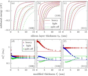
Then, we compute the energy levels at flat band, when the potential profile is a square
well and identify the type of each subband for different well widths. The results are shown
in Figure 2(a), (b), and (c) for (100), (110) and (111) device orientations, respectively. Next,
the quantization mass is extracted for each hole type as a function of t′
i by comparing the
numerical results with equation (3). The results are shown in Figure 2(d), (e), and (f): we
can see that as the layer thickness increases the data corresponding to different subbands
and silicon thicknesses collapse to a single curve for each hole type. The outcome is quite
similar to the case of the triangular well, with increasing confinement by thinner SOI layers
having a qualitatively similar effect to increasing the electric field in the bulk MOSFET.
The heavy hole mass is smallest for (100) devices, slightly bigger for (111) devices and much
larger for the (110) ones, especially for very small t′
i. For the thickest devices (i.e. weak
confinement), the effective masses reproduce the bulk values.
For both bulk MOSFETs and SOI devices the conclusions are very similar. For (100)
and (111) orientations the quantization mass of heavy holes essentially coincides with the
bulk mass in the h100i and h111i, respectively. The mass of light holes and split-off holes can depend on the transverse electric field or the Si layer thickness; in the (100) case the
variations are small because even the bulk masses values are similar to each other; in the
(111) case the variations are larger, but both values are quite smaller than the heavy hole
less populated. Therefore, for both (100) and (111) orientations, the bulk effective masses
could provide a good approximation. On the other hand, in the case of (110) orientation,
the bulk mass is recovered only for very weak confinement also for the heavy holes and
quite large values ofmq are obtained for moderate confinement. In this case we expect large
deviations if the bulk mass is used for models or simulations, and even a fitted value would
be suitable only in a limited range of transverse electric field values and SOI layer thickness.
III. EFFECTIVE MASS FOR THE DENSITY OF STATES
For electrons in two-dimensional parabolic subbands, the density of states gi(E) is
inde-pendent of energy
gi(E) =
mDOS
i
π¯h2 , (5)
and the occupation of a single valley reads (see for example16):
Ni =
KBT π¯h2 m
DOS
i ln
1 + exp
EF−Ei
KBT
, (6)
wheremDOS
i is the DOS effective mass, KB is the Boltzmann constant andEF is the energy of the Fermi level in the semiconductor. For ellipsoidal valleysmDOS
i can be directly computed
from the in-plane masses mx and my along the ellipse axes as mDOSi = √mxmy. In the case of hole subbands we can compute the density of states numerically from the dispersion
relationshipsEi(k) obtained by the self-consistent k·pcalculation. As an example, Figure 3 shows the energy dispersion E1(k) for the fundamental subband computed for MOSFETs
with the three considered surface orientations: (100), (110), and (111). The DOS obtained
from the numerical Ei(k) is not a constant: by directly inverting Equation (5) we would
obtain an energy-dependent mass, which would not be so useful. Instead, we can compute
mDOS
i by inverting the hole equivalent of equation (6) to obtain:
mDOSi =π¯h2Pi
KBT ln
1 + exp
Ei−EF
KBT
−1
, (7)
where we include the contribution of both spin states in the subband population Pi.
Figure 4(a) shows the results relative to a bulk MOSFETs as a function of inversion charge
density Pinv, while Figure 4(b) shows mDOS1 for double gate (DG) SOI devices as a function
oftSi. In both cases only the first subband is shown: we can observe the differences between
valence band structure under the different confining potential wells. In all cases the largest
mass is obtained for (100) substrate orientation, with a value almost equal to that of the free
electron mass. For (111) orientation mDOS
1 is smaller, and even smaller for (110) oriented
devices. We have to highlight that the DOS mass implies an average in the transport plane,
and it is not related to a single direction: in principle it cannot be related to the masses
of Table I and, indeed, the computed values cannot be deduced from the bulk ones. When
we consider the next subband the picture is even more complex: subband corresponding to
the same hole type have different masses because of band mixing and the interaction (and
crossings19) between different subbands at k 6= 0. For this reason and the fact that also
for the fundamental subband non-trivial variations are observed, we conclude that a single
value of a DOS mass cannot be provided, so that the effective mass approach cannot give
accurate results for the calculation of subband population.
IV. EFFECTIVE TRANSPORT MASS
A. Orientation dependence of low-field mobility of p-channel MOSFETs
The “mass” of heavy holes is larger than that of light holes; as a consequence, confinement
in MOS devices lifts their degeneracy (see Figures 1 and 2), so that the lowest energy (and
most populated) subband always correspond to heavy holes. Therefore, heavy holes give the
largest contribution to carrier properties, and in particular transport properties, especially
at high inversion densities. Then, considering the bulk heavy hole masses for transport in
theh100iandh110idirections,m= 0.27m0andm= 0.54m0, respectively (see Table I), one
can expect an important mobility difference between devices with h100i and h110i channel directions.
To test this experimentally, p-type MOSFETs were fabricated at KTH on 100 mm
di-ameter silicon wafers with (100) and (110) oriented surfaces. On each wafer, MOSFETs
were fabricated with channel directions along h100i, h110i, and a range of angles between these. Phosphorus implants formed the N-wells for the substrates, with an implant doses of
1×1013cm−2 at 300 keV. Dry thermal oxidation for 35 minutes at 700◦C was then used to
grow the SiO2 gate dielectric, on which N+ polysilicon was deposited to form the gate itself
implant-ing with 1×1015 cm−2 of boron at 4.5 keV. A 950◦C rapid thermal anneal for 30 seconds
followed to activate the dopants. Connections to the gate, source, drain and substrate and
their contact pads were formed by NiSi formation followed by sputtering TiW and then
Al. Gate oxide thicknesses of 3.9 nm and 6.3 nm were electrically measured for the (100)
and (110) p-MOSFETs, respectively, from the gate-channel capacitance in strong inversion.
A substrate doping concentration of ∼ 8×1016 cm−3 was measured from the gate-body
capacitance in depletion.
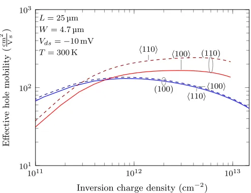
In Figure 5 we show the effective mobility measured on long channel n+/SiO2 gated
p-MOSFETs for (100) and (110) substrate orientations with h100i and h110i channel di-rections. The effective mobility, calculated from measurements of drain current and
gate-channel capacitance, is plotted as a function of inversion charge density. The inversion
charge density was calculated from the gate-channel capacitance using a measurement
fre-quency of 500 kHz. The frefre-quency was sufficiently high that the influence of interface traps
on the measurement was negligible. It was also sufficiently low to prevent distortion of the
capacitance profile at low inversion charge densities caused by the high channel resistance
attributed to the long channel length. In the measurement of the drain current, a drain bias
of −10 mV was used. This was low enough that the error caused by the finite drain bias could be neglected in extracting the mobility. Despite these precautions, there may still be
some error in the inversion charge density values calculated in the low density regime, with
corresponding uncertainty in mobility values in this region.
From the results shown in Figure 5, we conclude that for (100) devices hole mobility does
not depend on channel direction; it is almost the same for the h100i and h110i channels. By contrast, the hole mobility on the (110) substrate does depend on channel direction;
however, the mobility along theh100idirection is lower than that found for theh110ichannel orientation. This is the opposite to what one might expect given the masses of Table I,
although it is consistent with results obtained by others12. Therefore, we can conclude that
the bulk effective masses of Table I are not useful in order to understand the transport
properties of differently oriented devices, and that confinement direction must also be taken
B. Definition of the transport mass
For the transport mass, the most natural adaptation of the effective mass definition
to the case of two-dimensional subbands is obtained by substituting the direction in the
three-dimensional momentum space with the subband index (for quantum confinement)
and the direction in the two-dimensional parallel momentum space. Thus, given the energy
dispersion Ei(k) of subband i, the effective transport mass miα can be defined as: 1
mi α
= 1 ¯
h2
∂2Ei(k)
∂k2
α
, (8)
where kα is the momentum component in the transport direction α. If the dispersion were
parabolic, mi
α would be a constant for each subband i and direction α; however, this is not the case for the subbands computed employing thek·pmethod, whose energy dispersion is strongly anisotropic and non-parabolic. One could take the value atk = 0 as a representative
value18,20. However mi
α(k) can present strong variations as a function of k and, moreover, the functional dependence onkcan depend on the confining potential (silicon layer thickness
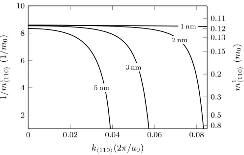
in SOI devices and applied bias). As an example, Figure 6 shows m1
h110i along the h110i
direction for (110) oriented SOI devices with different silicon thicknesses. There are strong
variations in the effective mass, which get larger for the thicker devices: the behavior strongly
depends on tSi, while the value at k= 0 only presents a weak dependence. This means that
the different behavior one expects due to the differences in the energy dispersion is not
captured by the value of m1
h110i at k= 0.
When we consider the wave-vector k in the whole two-dimensional transport plane the
picture is even more complex, as shown in Figure 7. Figures 7(a) and (b) show the inverse
effective mass computed as in Equation (8) for a SOI device (tSi = 2 nm) with (100)
orienta-tion and h100i and h110itransport direction, respectively. The values near the Γ point are similar in the two cases, while in the rest of the k-plane the behavior is completely different
and the variations of effective mass even in a relatively small region are important.
Fig-ures 7(c) and (d) show the same quantity for a (110) substrate and the sameh100iandh110i directions: again, the variations are very strong and the behavior is completely different.
Finally, Figures 7(e) and (f) correspond to devices with the same (110) orientation andh110i channel as in (d) but with tSi = 3 nm and tSi = 5 nm, respectively. The value near the Γ
point is similar in the three cases, while the behavior in the rest of thek-plane is different, as
account the contribution of all the occupied region of momentum space at equilibrium, we
define an average effective transport mass Mi
α, where the weight is given by the occupation probability. We obtain21:
1 Mi α = 1 mi α =
Z f(E
i(k))
mi α
dk
, Z
f(Ei(k))dk, (9)
where f(E) is the Fermi-Dirac distribution function.
An important observation is thatMi
α does not depend on the directionαin the transport plane when substrate orientation is (100) or (111). For example, for (100) devices, Mi
[010]
and Mi
[001] coincide for symmetry reasons. Then we have
1 Mi α =1 ¯ h2
∂2E
i(k)
∂k2 α i =1 ¯ h2 *
∂2E
i(k)
∂k2 [010]
+
i
cos2α+ 1 ¯
h2
*
∂2E
i(k)
∂k2 [001]
+
i
sin2α+ 1 ¯
h2
∂2E
i(k)
∂k[010]∂k[001]
i
cosαsinα
= 1
Mi
[010]
cos2α+ 1
Mi
[001]
sin2α
= 1
Mi
h100i ,
(10)
where the average of the mixed derivative vanishes for symmetry reasons and the last line
follows from the fact that Mi
[010] = M[001]i = Mhi100i. An analogous proof is possible in
the case of (111) surface orientation. This fact can explain the very small dependence on
channel orientation observed for the mobility on (100) substrates shown previously. Taking
into account the observed difference between mi
h100i and mih110i as functions of k, as shown
in Figures 7(a) and (b), we can conclude that averaging is crucial in order to obtain the
in-plane isotropic behavior of Mi α.
We stress that the proposed averaging procedure is different from the one proposed in
Ref.12 to explain similar experimental results. In that case, the authors calculated the
effective mass (Equation (8)) atk= 0 for all directionsαand then averaged overα, justifying
such average by the fact that in near equilibrium (long channel devices) all two-dimensional
momentum space must contribute to the “sampled” effective mass. On the contrary, we
calculate the directional derivative as a function ofk for a givenα and average these values
the wave-vector k can take every direction in the transport plane, but α is fixed because it
represents the channel direction, i.e. the direction of the drift electric field: the (second)
derivative along a given directionαrepresents the effect that an electric field in such direction
has on the motion of a carrier with given wave-vector k.
In Figure 8, we showM1
h100i andMh1110i computed according to equation (9), for p-channel
MOSFETs with (100) and (110) substrate orientations, as a function of inversion carrier
density. Comparing these results with the measured effective mobility of Figure 5, we
can see that the average effective mass is useful in order to interpret the experimental
results. Firstly, we note that in the high inversion charge density region, where practical
devices operate, the mass is significantly lower for (110) orientated substrates than for (100)
orientation. This can directly explain the enhanced mobility observed on (110), which has
previously been attributed to reduced scattering arising from a greater subband splitting
between light and heavy holes. Secondly, for (100) substrate orientation, the transport mass
does not depend on channel direction, as expected from symmetry arguments. Thirdly, for
(110) orientation, the transport mass is lower for both channel directions: in particular,
M1
h110i is lower thanMh1100i (except at very low inversion charge density) and this fact agrees
with the higher mobility observed for the h110i channel. Moreover, the masses for the two directions get closer to each other at small values of inversion charge, where the mobility
values also converge. This analysis is not fully comprehensive, because it only takes into
account the first subband of heavy holes, but shows that the average transport mass defined
in equation (9) is useful for the interpretation of transport properties near equilibrium.
C. Simulation study of hole mobility of ultra-thin SOI devices
Now, we turn to ultra-thin SOI devices and consider the dependence of hole mobility on
orientation and Si film thickness, and its relation to the transport effective mass. To do so,
we simulate different symmetric DG SOI structures with silicon layer thicknesses, tSi, ranging
from 1 to 15 nm; the channel is considered essentially undoped (ND = 1×1014 cm−3), the thickness of both oxide layers istox= 1 nm, and a midgap metal is used as a gate material.
We compute the hole mobility,µ, employing the Kubo-Greenwood formula22, employing the
subband dispersion and wavefunctions obtained with the 6 bandk·pmodel, as in Ref.14. We
mechanisms23.
The dependence of hole mobility ontSiis shown in Figure 9, for different values of inversion
carrier density Pinv. We only represent one curve for (100) and (111) surface orientations,
because in these casesµshows a very small dependence (up to 1–2%) on channel orientation,
whereas a large mobility difference is observed between different channel orientations for
(110) devices. It is clear that for very thin channels µis always strongly reduced; however,
it is important to emphasize that there are large quantitative differences between curves
corresponding to different surface and channel orientations. The most important observation
is that hole mobility is severely degraded for (100) devices below 6 nm, while this happens
at smaller values of tSi for (110) and (111) devices. Therefore, the mobility enhancement of
alternative orientations not only persists for ultra-thin devices; on the contrary, it increases
and can be quite large, especially at small values of Pinv. To study the origin of such
enhancement we separate the mobility of the first two subbands, as shown in Figure 10. The
important mobility decrease can be attributed to the increase of both phonon and surface
roughness (SR) scattering at small Si thickness. One difference that Figure 10 highlights at
small tSi is an enhanced mobility in the second subband for (111) orientation compared to
(100), which may go someway to explaining the shape of Figure 9. This is less pronounced
for (110). However, the different behavior corresponding to different surface orientations
cannot be fully explained by differences in the scattering rates21.
Figure 11 showsm1
α computed at k = 0 and Mα1 as functions of tSi; while the former has
a weak dependence on tSi for all orientations, the latter shows a strong decrease at small tSi
for (110) surface orientation, especially for the h110i direction. This fact compensates, to a certain extent, the large increase of scattering rates (both from phonons and SR) occurring
at very small thicknesses, giving rise to the mobility behavior shown in Figures 9 and 10.
Such a decrease of M1
α is not caused by a corresponding decrease in m1α(0) but, as we can
see in Figures 7(d), (e), and (f) by a flattening of the surface ofm1
α(k). Figure 11 also shows that Mi
α for (110) substrate orientation is lower than (100) or (111) orientations and that, in this case, it depends on the transport direction: in particular the effective mass for the
h110i channel is much lower (and consequently the mobility is larger) than for the h100i channel.
To conclude this section, we can say that the mobility advantage of (110) over (100)
structures. The behavior of the transport mass, defined with the proper averaging procedure,
is very useful in interpretting this result.
V. CONCLUSIONS
We have explored the chance to define an effective mass for hole transport for both bulk
and ultra-thin SOI inversion layers, and we have also provided a procedure to evaluate such a
parameter, when it is possible. We have shown how to compute the quantization mass, DOS
mass and transport mass for holes in bulk and SOI MOSFETs; in particular, the transport
mass can be related to transport properties only if proper averaging is taken into account.
The “bulk” hole mass can be used as the quantization mass only for heavy holes in devices
with (100) and (111) orientations. In the cases of DOS and transport mass there is no direct
relationship with the “bulk” ones, and those must be computed from the numerical band
structure. The results can be used to explain why hole transport is most favorable for a
h110i directed channel on a (110) orientated substrate.
ACKNOWLEDGMENTS
This work was partially supported by the EU EUROSOI+ Thematic Network
(FP7-CA-216373) and “NANOSIL” Network of Excellence (FP7 IST-216171). The work of L.D.
is done as part of the program Ram´on y Cajal of the Ministerio de Ciencia e Innovaci´on
(M.C.I.) of Spain. Financial support from M.C.I. (contracts TEC2008-06758-C02-01 and
FIS2008-05805), Junta de Andaluc´ıa (project TIC-P06-1899).
1 M. V. Fischetti and S. E. Laux, Physical Review B48, 2244 (1993).
2 C. Jungemann, A. Emunds, and W. Engl, Solid-State Electronics36, 1529 (1993).
3 K. Uchida, A. Kinoshita, and M. Saitoh, inElectron Devices Meeting, 2006. IEDM ’06.
Inter-national (2006) pp. 1–3.
4 K. Hess,Monte Carlo device simulation: full band and beyond (Kluwer, 1991).
5 A. Abramo, L. Baudry, R. Brunetti, R. Castagne, M. Charef, F. Dessenne, P. Dollfus, R.
C. Hamaguchi, K. Hess, K. Hennacy, P. Hesto, J. Higman, T. Iizuka, C. Jungemann, Y.
Ka-makura, H. Kosina, T. Kunikiyo, S. Laux, H. Lin, C. Maziar, H. Mizuno, H. Peifer, S.
Ra-maswamy, N. Sano, P. Scrobohaci, S. Selberharr, M. Takenaka, T. Tang, K. Taniguchi, J.
Tho-bel, R. Thoma, K. Tomizawa, M. Tomizawa, T. Vogelsang, S. Wang, X. Wang, C. Yao, P. Yoder,
and A. Yoshii, IEEE Transactions on Electron Devices41, 1646 (1994).
6 M. V. Fischetti and S. E. Laux, Physical Review B38, 9721 (1988).
7 J. M. Luttinger and W. Kohn, Physical Review97, 869 (1955); J. M. Luttinger,ibid.102, 1030
(1956).
8 J. R. Chelikowsky and M. L. Cohen, Physical Review B14, 556 (1976).
9 M. De Michielis, D. Esseni, Y. Tsang, P. Palestri, L. Selmi, A. O’Neill, and S. Chattopadhyay,
Electron Devices, IEEE Transactions on54, 2164 (2007).
10 T. Mizuno, N. Sugiyama, T. Tezuka, Y. Moriyama, S. Nakaharai, T. Maeda, and S. Takagi, in
IEEE International Electron Devices Meeting, Tech. Dig. 2003 (2003) pp. 33.6.1– 33.6.4.
11 S. Takagi, M. Takayanagi, and A. Toriumi, Electron Devices, IEEE Transactions on 46, 1446
(1999).
12 S. Saito, D. Hisamoto, Y. Kimura, N. Sugii, R. Tsuchiya, K. Torii, and S. Kimura, in VLSI
Technology, 2006. Digest of Technical Papers. 2006 Symposium on (2006) pp. 150–151.
13 A. Rahman, M. S. Lundstrom, and A. W. Ghosh, Journal of Applied Physics97, 053702 (2005).
14 L. Donetti, F. Gamiz, and N. Rodriguez, Semiconductor Science and Technology 24, 035016
(2009).
15 M. V. Fischetti and S. E. Laux, Journal of Applied Physics80, 2234 (1996).
16 F. Stern and W. E. Howard, Physical Review 163, 816 (1967).
17 Only in this case we do not impose self-consistency in our simulations; energy levels are
com-puted for triangular well with varying electric field and for different quantization directions.
18 Y. Kajikawa, Journal of Applied Physics106, 063712 (2009).
19 Y. Zhang, J. Kim, and M. Fischetti, Journal of Computational Electronics 7, 176 (2008).
20 E. Wang, P. Matagne, L. Shifren, B. Obradovic, R. Kotlyar, S. Cea, M. Stettler, and M. Giles,
Electron Devices, IEEE Transactions on53, 1840 (2006).
21 L. Donetti, F. G´amiz, N. Rodr´ıguez, F. Jim´enez-Molinos, and J. Rold´an, Solid-State Electronics
TABLE I. Effective masses computed for bulk Si with the 6-band k·pmodel for different channel directions.
h100i h110i h111i
heavy holes 0.274 0.541 0.668
light holes 0.204 0.149 0.142
split off holes 0.234 0.234 0.234
−0.3
−0.2
−0.1
0
subband
energy
(eV)
heavy light split-off
104
105
106
0.1 1
m
q 1
(
m
0
)
heavy light split-off
104
105
106
transverse electric fieldF (V/cm)
104
105
106
(100) (110)
(111)
(100) (110) (111)
(a) (b) (c)
(d) (e) (f)
FIG. 1. (Color online) Energy level and quantization mass for holes in a triangular well, as a
function of the transverse electric field for surface orientations (100), (110) and (111).
22 M. V. Fischetti, Z. Ren, P. M. Solomon, M. Yang, and K. Rim, Journal of Applied Physics94,
1079 (2003).
23 L. Donetti, F. Gamiz, N. Rodriguez, A. Godoy, and C. Sampedro, Journal of Applied Physics
[image:17.595.68.534.113.457.2]0 5 10 15 −0.3
−0.2
−0.1
0
subband
energy
(eV)
0 5 10 15
silicon layer thicknesstSi(nm)
heavy light split-off
0 5 10 15
0 5 10 15
0.1 1 m q i ( m 0 ) heavy light split-off
0 5 10 15
modified thicknesst′
i(nm)
0 5 10 15
(100)
(110)
(111)
(100) (110) (111)
(a) (b) (c)
(d) (e) (f)
FIG. 2. (Color online) Energy level and quantization mass for SOI devices, as a function of the
silicon layer thickness for different surface orientations.
−0
.2 0 0.2
−0
.2
0 0
.2
k[010](2π/a0)
k[001] (2 π /a 0 ) −0
.2 0 0.2
k[001](2π/a0)
k[1 ¯ 10] (2 π /a 0 ) −0
.2 0 0.2
k[11¯2](2π/a0)
k[1 ¯ 10] (2 π /a 0 ) 0 50 100 150 200 E1 (meV)
(100) (110) (111)
FIG. 3. (Color online) Energy dispersion E1(k) for the fundamental subband in (100), (110), and
(111) MOSFETs with inversion density Pinv = 6×1012 cm−2. The energy difference between
[image:18.595.158.456.75.331.2] [image:18.595.88.529.444.586.2]1011 1012 1013
0 0.2
0.4
0.6
0.8
1
(100)
(111)
(110) (a)
inversion density (cm−2
)
ground
sub
band
DOS
mass
(
m
0
)
0 5 10 15
0 0.2
0.4
0.6
0.8
1
(100)
(111)
(110)
dotted:Pinv= 1×10
13cm−2
solid: flat band (b)
silicon layer thickness (nm)
FIG. 4. (Color online) DOS effective mass of the fundamental subband of bulk MOSFETs (a) and
DG SOI devices (b).
1011 1012 1013
101
102
103
h110i h100i
(100)
h100i h110i (110)
L= 25µm W= 4.7µm Vds=−10 mV
T= 300 K
Inversion charge density (cm−2
)
Effectiv
e
hole
mobil
it
y
(
cm
2
V
s
)
FIG. 5. (Color online) Hole effective mobility as a function of inversion charge density, for (100)
[image:19.595.156.458.75.231.2] [image:19.595.184.431.423.613.2]0 0
.02 0.04 0.06 0.08
2 4 6 8 10
5 nm 3 nm
2 nm 1 nm
kh110i(2π/a0)
1
/m
1 h110
i
(1
/m
0
)
0
.8
0
.5
0
.3
0
.2
0
.15
0
.13
0
.12
0
.11
m
1 h110
i
(
m
0
[image:20.595.182.430.73.231.2])
FIG. 6. Transport mass m1
h110i of the first subband along h110i direction for (110) oriented SOI
−4 −2 0 2 4 ky (1 0 6 cm − 1 ) (a) (b) −4 −2 0 2 4 ky (1 0 6 cm − 1 ) (c) (d) −4 −2 0 2 4 ky (1 0 6 cm − 1 )
−4 −2 0 2 4
kx (10
6
cm−1
) (e)
−4 −2 0 2 4
kx (10
6
cm−1
) (f) 0 1 2 3 4 5 6 7 8 9 1 /m
1 (α
k ) (1 /m 0 )
FIG. 7. (Color online) Transport mass m1α as a function of k for the following SOI devices:
tSi= 2 nm with (100) surface orientation andkαparallel to h100i(a), (100)/h110i (b), (110)/h100i
(c), (110)/h110i (d); (e) and (f) are the same as (d) but with tSi = 3 nm and 5 nm, respectively.
For (100) orientationkx and ky are directed along [010] and [001], while for (110) orientation they
[image:21.595.124.485.74.517.2]1011 1012 1013
0 0
.2
0
.4
0
.6
0
.8
100/any
110/h100i
110/h110i
Inversion charge density (cm−2
)
M
1 α
(
m
0
)
FIG. 8. (Color online) Average hole transport massMα1 of the first subband along h100i andh110i
directions for (100) and (110) oriented p-MOSFETs.
101
102
103
Pinv= 5×10
12
cm−2
(a)
mobilit
y
µ
(
cm
2
V
s
)
(100) (110)/h001i
(111) (110)/h110i
0 2 4 6 8 10 12 14 16 101
102
103
Pinv= 2×10
13cm−2
(b)
silicon layer thicknesstSi (nm)
mobilit
y
µ
(
cm
2
V
s
)
FIG. 9. (Color online) Calculated hole mobility as a function oftSifor different surface orientations
[image:22.595.186.430.71.256.2] [image:22.595.194.414.424.629.2]101
102
103
5×10¹²
cm−2
i= 1
(a) µi ( cm 2 V s )
5×10¹²
cm−2
i= 2
(b)
0 2 4 6 8 101
102
103
2×1013cm−2
i= 1
(c)
tSi(nm)
µi ( cm 2 V s )
0 2 4 6 8 2×1013cm−2
i= 2
(d)
tSi(nm)
FIG. 10. (Color online) Calculated mobility of holes in the first and second subbands. Line types
and colors represent surface orientations and channel directions as in Figure 9.
1 0.6 0.4 0.3 0.2 0.15 0.12 (110)/h110i (110)/h001i (100)/h011i (111)/h112i m
α|1
k =0 ( m 0 ) 2 4 6 8 1 / m α 1 |k =0 (1 /m 0 )
1 2 3 4 5 6 7 8 1
0.6 0.4 0.3 0.2 0.15 0.12
(110)/h110i
(110)/h001i
(100)/h011i (111)/h112i
solid: Pinv= 5×10
12cm−2
dashed: Pinv= 2×10
13
cm−2
tSi(nm)
M 1 α ( m 0 ) 0 2 4 6 8 1 /M 1 α (1 /m 0 )
FIG. 11. (Color online) Effective masses m1
α(0) and Mα1 as a function of tSi for SOI devices with
[image:23.595.187.423.70.269.2] [image:23.595.182.428.379.650.2]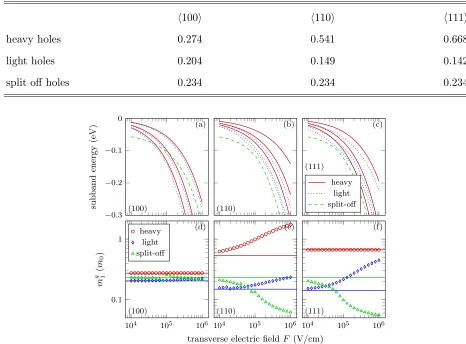
![FIG. 7.(Color online) Transport massFor (100) orientationare directed along [001] and [1t(c), (110)/ m1α as a function of k for the following SOI devices:Si = 2 nm with (100) surface orientation and kα parallel to ⟨100⟩ (a), (100)/⟨110⟩ (b), (110)/⟨100⟩⟨11](https://thumb-us.123doks.com/thumbv2/123dok_us/9658834.467934/21.595.124.485.74.517/transport-orientationare-directed-function-following-surface-orientation-parallel.webp)


