University of Warwick institutional repository:http://go.warwick.ac.uk/wrap
A Thesis Submitted for the Degree of PhD at the University of Warwick
http://go.warwick.ac.uk/wrap/77508
This thesis is made available online and is protected by original copyright. Please scroll down to view the document itself.
Development and Application of
Electrochemical Scanning Probe
Microscopy Techniques for Studying
Interfacial Processes
by
Sophie Laura Kinnear
Thesis
Submitted to the University of Warwick
for the degree of
Doctor of Philosophy
Department of Chemistry
Contents
List of Tables vii
List of Figures viii
Abbreviations xi
Glossary of Symbols xiii
Acknowledgments xv
Declarations xvii
Abstract xviii
Chapter 1 Introduction 1
1.1 An Overview of Surface Science and Electrochemistry . . . 2
1.2 Scanning Probe Microscopy . . . 4
1.2.1 Atomic Force Microscopy . . . 5
1.2.2 Scanning Electrochemical Microscopy . . . 7
1.2.3 Scanning Ion Conductance Microscopy . . . 10
1.2.4 Scanning Electrochemical Cell Microscopy . . . 14
1.3 Ionic Crystals and Crystal Dissolution . . . 19
1.3.1 Mechanisms for Crystal Dissolution . . . 19
1.3.2 Defects in Crystal Structure . . . 22
1.4 Previous Techniques for Studying Crystal Dissolution . . . 22
1.4.1 Batch Technique . . . 23
1.4.2 Hydrodynamic Control Techniques . . . 23
1.5 Surface Charge and the Electric Double Layer . . . 26
1.5.1 Current Methods for Probing Surface Charge . . . 29
1.5.2 Surface Charge Mapping . . . 31
1.6 Aims of this Thesis . . . 32
Chapter 2 Experimental Methods and Instrumentation 34 2.1 General Materials . . . 34
2.1.1 Solutions . . . 35
2.2 Probe Fabrication . . . 36
2.2.1 Capillary Probes . . . 36
2.2.2 Ultramicroelectrodes . . . 38
2.3 Characterisation Techniques . . . 40
2.3.1 Atomic Force Microscopy . . . 40
2.3.2 Scanning Electron Microscopy . . . 40
2.4 Electrochemical Scanning Probe Microscopy Instrumentation . 41 2.4.1 Probe and Sample Movement . . . 42
2.4.2 Signal Generation and Collection Hardware . . . 42
2.4.3 Lockin Amplifiers . . . 43
2.4.4 Shielding . . . 44
2.5 Data Analysis Using MATLAB . . . 45
Chapter 3 Development of the LabVIEW Code for Scanning Probe Microscopes 48 3.1 Field Programmable Gate Array Cards . . . 50
3.2 Waypoint Instructions . . . 52
3.3 The Host Program . . . 53
3.4 The Target Program . . . 54
3.4.1 Waypoint Output Loop . . . 54
3.4.2 Data Acquisition Loop . . . 55
3.5 Temporary and Permanent Data Saving . . . 58
3.6 Scanning Programs . . . 58
3.7 Example Program . . . 60
3.8 Features . . . 61
3.8.1 Real Time Data Viewing . . . 61
3.8.3 Self-Referencing Setpoint . . . 64
3.8.4 Motorised Coarse Positioners . . . 65
3.8.5 Auto-Scaling Bipotentiostat . . . 65
3.9 Acknowledgements . . . 66
3.10 Tables . . . 67
Chapter 4 Dual-Barrel Conductance Micropipette as a New Ap-proach to the Study of Ionic Crystal Dissolution Kinetics 75 4.1 Introduction . . . 76
4.2 Experimental Section . . . 78
4.2.1 Analytical Methodology . . . 78
4.2.2 Finite Element Method Modeling . . . 80
4.3 Results and Discussion . . . 83
4.3.1 Ion Conductance Measurements . . . 83
4.3.2 Simulations and Modeling . . . 86
4.3.3 Dissolution Pit Morphology Measurements . . . 91
4.4 Conclusions . . . 93
4.5 Acknowledgements . . . 94
Chapter 5 Targeted Dissolution of Calcite on the Microscale using the Dual-Barrel Conductance Micropipette Technique: Kinetics and Patterning 95 5.1 Introduction . . . 96
5.2 Experimental . . . 98
5.2.1 Materials and Solutions . . . 98
5.2.2 Instrumentation . . . 99
5.2.3 Methodology . . . 99
5.2.4 Finite Element Method Model . . . 100
5.2.5 Crystallography . . . 101
5.3 Results and Discussion . . . 103
5.3.1 AFM Measurements of Etch Pits . . . 103
5.3.2 Simulations . . . 104
5.3.3 Raster Scanning . . . 107
5.3.4 Patterning . . . 110
5.5 Acknowledgements . . . 113
Chapter 6 Surface Charge Mapping with a Nanopipette 114 6.1 Introduction . . . 115
6.2 Methods . . . 118
6.2.1 Substrates . . . 118
6.2.2 Instrumentation . . . 118
6.2.3 SICM Approach Curves . . . 119
6.2.4 SICM Maps . . . 120
6.2.5 Atomic Force Microscopy . . . 121
6.2.6 Simulations . . . 121
6.3 Results and Discussion . . . 121
6.3.1 Approach Curves . . . 121
6.3.2 Surface Charge Mapping . . . 133
6.4 Conclusions . . . 136
6.5 Acknowledgements . . . 138
Chapter 7 Dynamic Nanoscale Surface Charge Mapping at Ul-tramicroelectrodes 139 7.1 Introduction . . . 139
7.2 Experimental . . . 140
7.2.1 Electrodes . . . 140
7.2.2 Nanopipettes . . . 141
7.2.3 Bias Modulated-Scanning Ion Conductance Microscopy Instrumentation . . . 141
7.2.4 Impedance . . . 143
7.2.5 Experimental Methodologies . . . 144
7.3 Results and Discussion . . . 144
7.3.1 Approach Curves and CVs . . . 144
7.3.2 Dynamic Surface Charge Mapping . . . 148
7.4 Conclusion . . . 148
7.5 Acknowledgements . . . 151
List of Tables
2.1 List of all chemicals and materials used in this thesis. . . 35
2.2 List of rigs and their permanent features . . . 41
2.3 Breakout box description . . . 44
2.4 Rig hardware list . . . 47
3.1 Waypoint Cluster . . . 67
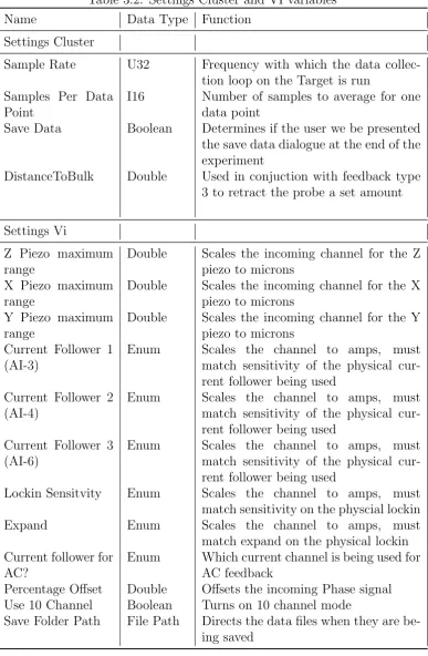
3.2 Settings Cluster and VI variables . . . 68
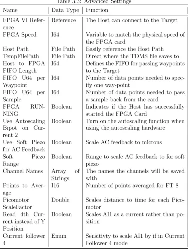
3.3 Advanced Settings . . . 69
3.4 Change on Fly Cluster . . . 70
3.5 Static Variables currently on the Target . . . 71
3.6 Dynamic variables current on the Target . . . 72
3.7 Feedback Types . . . 73
3.8 Channel names . . . 73
3.9 Display Cluster . . . 74
List of Figures
1.1 Schematic of two reference electrodes . . . 4
1.2 Diagram and force curve of AFM . . . 6
1.3 Diagrams of SECM modes of operation . . . 8
1.4 Schematic of SICM modes and approach curves . . . 12
1.5 Schematic diagram of the dual barrelled conductance micropipet 15 1.6 Diagram of mass transport and surface processes . . . 21
1.7 Double layer diagram of Helmholtz and Gouy-Chapman models 27 1.8 Double layer diagram of the Stern and BDM models . . . 29
2.1 Theta capillary laser pulling process . . . 37
2.2 Diagram of a UME and the setup for performing inverted UME experiments . . . 39
2.3 Photo of a typical rig setup inside and outside of the Faraday cage . . . 43
3.1 Flow chart of waypoints and data . . . 51
3.2 Schematic of the Host . . . 53
3.3 Schematic of the Target . . . 56
3.4 Two basic scanning patterns . . . 59
3.5 Front panel of the Approach Then CV program . . . 61
3.6 Block diagram of the Approach Then CV program . . . 62
4.1 Schematic of the setup for NaCl dissolution . . . 79
4.2 Simulation domain of NaCl FEM Model . . . 82
4.5 Probe composition profiles from the FEM model of the dissolu-tion of NaCl . . . 88 4.6 Results from the FEM model of the dissolution of NaCl in a
dual barrel micropipet . . . 89 4.7 Results from the FEM model of the dissolution of NaCl in a
dual barrel micropipet . . . 90 4.8 AFM image of pits formed during dissolution of NaCl . . . 92
5.1 Schematic of the experimental and simulation setup for Calcite dissolution . . . 98 5.2 Comparison of washed and unwashed calcite etch pits . . . 103 5.3 AFM images of etch pits and the volume vs time graph . . . . 105 5.4 Graphs of etch time vs pit parameters . . . 106 5.5 Comparison of experimental and simulated ion current for
cal-cite dissolution . . . 107 5.6 Profiles of concentration and electric potential from the steady
state model . . . 108 5.7 Working curve from the FEM model showing surface flux,
dis-solution rate constant and meniscus contact radius . . . 109 5.8 Laue and CrystalMaker images of the calcite surface . . . 110 5.9 AFM image and line profile of a typical raster scan and a
dia-gram of the scan directions . . . 111 5.10 Top view of the (104) face where A) shows the two exposed
obtuse steps, moving the probe in these directions results in wide, shallow pits. B) shows the acute step adjacent to only one obtuse step, moving the probe towards the acute steps results in constricted dissolution and narrow deep pits. . . 112 5.11 AFM image of the word CALCITE etched into the crystal . . 112
6.1 Schematic of an SICM probe for Surface Charge Mapping . . . 116 6.2 Piezoelectric positioner extension for the purposes of thermal
drift detection . . . 120 6.3 Typical current-potential response of a nanopipette of 60 nm
6.5 Schematic of the DDL and direction of cation transport . . . . 125 6.6 Schematics of cation mass transport flux and perm-selective
re-gions at the negatively charged nanopipette, and substrates of different charge (on the left of each part) and FEM simulation results (on the right of each part) of the resulting ion concen-trations near the end of a nanopipette at surfaces . . . 128 6.7 Normalized AC ion current magnitude over (A) glass, (B) polystyrene
and (C) APTES . . . 129 6.8 Polar plots of phase change with respect to AC for approaches
over (A) glass, (B) polystyrene and (C) APTES . . . 131 6.9 Two-dimensional hopping mode SICM images of a glass
sub-strate partially covered with a thin polystyrene film. . . 135 6.10 Hopping mode images, with 1 µm resolution, of a PLL spot
(positively charged) on a glass substrate (negatively charged) . 137
7.1 Setup and details of the three electrode system for measuring surface charge on a UME . . . 142 7.2 Impedance spectroscopy plot of capacitance at liquid-liquid
in-terface between a hemispherical Hg electrode and supporting electrolyte KNO3 in three different concentrations. . . 145 7.3 Approach curves and CVs on the UME . . . 146 7.4 Four frames from a image sequence (of maximum 582 frames)
showing a CV applied to a Hg electrode and the topography of the sample . . . 149 7.5 Four frames from a image sequence showing a CV applied to a
Abbreviations
AFM Atomic Force Microscopy APTES (3-aminopropyl)triethoxysilane
BDM Bockris, Devanathan, and M¨uller Model BM Bias Modulation
BNC Bayonet NeillConcelman
C-AFM Conductive Atomic Force Microscopy CFC Channel Flow Cell
CV Cyclic Voltammetry DDL Diffuse Double Layer DM Distance Modulation
EBSD Electron Backscatter Diffraction EDL Electric Double Layer
FE-SEM Field Emission - Scanning Electron Microscopy FIB Focused Ion Beam
FIFO First In First Out
FPGA Field Programmable Gate Array FT Feedback Type
HAP Calcium Hydroxyapatite
HOPG Highly Orientated Pyrolytic Graphite I16 16 Bit Signed Integer
IC-SECM Intermitant Contact - Scanning Electrochemical Microscopy IT Current-Time
LSV Linear Sweep Voltammetry PLL Poly-L-Lysine
PSD Phase Sensitive Detector PZC Potential of Zero Charge
QRCE Quasi-Reference Counter Electrode RD Rotating Disc
SAM Self Assembled Monolayer
SECCM Scanning Electrochemical Cell Microscopy SECM Scanning Electrochemical Microscopy SG-TC Substrate Generation - Tip Collection SHE Standard Hydorgen Electrode
SICM Scanning Ion Conductance Microscopy SIR Surface Induced Retification
SPIP Scanning Probe Image Processing SPM Scanning Probe Microscopy STM Scanning Tunnelling Microscopy SVN Subversion
SWNT Single Walled Carbon Nanotube TDMS Technical Data Management System TG-SC Tip Generation - Substrate Collection U64 64 Bit Unsigned Integer
Glossary of Symbols
Symbol Common Units Description
A V Amplitude
An - New value to average
Asum - Sum of average values CB mM Bulk concentration
c mM Concentration
c∗ mM Starting concentration
Csat M Saturation concentration Db mm2s−1 Diffusion coeffiecnt
Dr Hz Data collection rate of FPGA card e C Charge on an electron
Eb V Potential difference between barrels
f Hz Frequency
h J Planck’s Constant
ib A Conductance current
J A m−2 Current density vector
j mm2s−1 Diffusional flux
k mm2s−1 Dissolution flux K J K−1 Boltzman Constant
N mm2s−1 Flux vector
n - Inward unit vector
N - Number of data points to average P - Proportional Factor
rp nm Radius perpendicular to the septum rt nm Radius parelle to the septum
t s Time
T K Temperature
tw nm Septum width
ui S m−1 Ionic conductivity of species i
x nm distance
z C Charge of speices
α - Slope of the current distance curve
ε F m−1 Dielectric constant
θ ◦ Semi-angle of pipet
κ m−1 Inverse thickness of the double layer
σ S m−1 Solution conductivty
σm C m−2 Charge density φ V Applied potential
ϕ ◦ Phase shift
φ0 V Potential offset from pzc
Acknowledgments
I would like to express my gratitude to all the members of Warwick Electro-chemistry and Interfaces Group, past and present. These four years have been an amazing experience of learning and working with you all. The group has really felt like a family, for good and bad! To the people in my year, this has been a fantastic journey to go on with you guys, thanks to Binoy Nadappuram, Jenny ‘I spin my web in order to protect you’ Webb and Changhui ‘Hui’ Chen and thanks to Barak Aaronson for always providing a challenge. Of course, I would also like to thank Rob Channonball for being a complete and utter dude, I still remember meeting you and Cat in first year of undergrad!
as part of the QUANTIF fund.
My friends outside of uni played a vital role in not letting me go crazy so many thanks to all my hundreds of housemates from Acorn House, I have learnt something from all of you, even if it was only how live with basically anyone. I hope you all keep being awesome and that the Acornmas tradition continues. I am grateful to all members of the Kali-JKD society and of course our exceptional instructor, Lucky, for some fantastic years of effective stress relief and good fun. In the last few difficult months, my thanks go to the people who were around and looking out for me, Paul Long and Miri Volger, in particular. Special thanks go to Helen Cockerton and Philip Carter, I hope our friendship lasts however far apart we end up and, of course, to my dear friend, Rehab Al Botros, whose amazing courage in the face of adversity has given me so much strength and perspective in my own troubles.
Most importantly, I am grateful to my interesting family who have been a never ending supply of support and humour. Thanks to my brother Tim, especially for LATEX advise, my sisters Amy and Hayley, my dogs Rocky, Sally,
Jack and Ollie and my parents Michael and Natalie. Lastly, so much thanks to my partner, Adam, whose love and support has been truly remarkable.
I relied heavily on the Inkscape program, so I would like thank all the developers that made such a great program for free use. This thesis was typeset with LATEX 2ε1 by the author.
1LA
TEX 2ε is an extension of LATEX. LATEX is a collection of macros for TEX. TEX is
Declarations
This thesis is submitted to the University of Warwick in support of my ap-plication for the degree of Doctor of Philosophy. It has been composed by myself with the exception of the list below and has not been submitted in any previous application for any degree.
Chapter 3: The majority of the WEC-SPM project code was written by Dr. Kim McKelvey.
Chapter 4: All FEM data was obtained by models from Dr. Michael Snowden and Dr. Kim McKelvey. The work discussed in this chapter has been published: Sophie L. Kinnear, Kim McKelvey, Michael E. Snowden, Massimo Peruffo, Alex W. Colburn and Patrick R. Unwin, Langmuir, 29, 15565
Chapter 5: All data from FEM models and CrystalMaker was obtained by Rehab Al Botros. Dr. Monica Ciomaga Hatnean performed all Laue X-ray crystallography used in this chapter.
Chapter 6: All data from FEM models was obtained by Kim McKelvey. The work discussed in this chapter has been published: Kim McKelvey, Sophie L. Kinnear, David Perry, Dmitry Momotenko and Patrick Unwin, J. Am. Chem. Soc 136, 13735
Abstract
Chapter 1
Introduction
“The famous pipe. How people reproached me for it! And yet,
could you stuff my pipe? No, it’s just a representation, is it not?
So if I had written on my picture ‘This is a pipe’, I’d have been
lying!”
Rene Magritte
1.1
An Overview of Surface Science and
Electrochemistry
Surface (or interfacial) science, very broadly, is the study of reactions and phe-nomena at the interface between two phases. These phases can be a liquid-gas interface, like the exchange of CO2 in air to HCO3– in an aqueous solution due to the accompanying chemical reaction, a liquid-liquid layer of two im-miscible fluids or, as will be the focus of this body of work, a solid in contact with a solution. Surface science also defines a large field where well-defined single crystals of metals or semiconductors are studied in ultra high vacuum. Common examples for surfaces that might be studied include an electrode with an externally applied potential in contact with a salt solution or a crystal immersed in an undersaturated solution prompting dissolution. Although the work herein does not have a focus on the more common use of electrochemistry, namely redox reactions, understanding the kinetics and behaviour of species under a potential field and at electrode surfaces is of paramount importance and is dealt with in this thesis.
An appropriate starting point when discussing electrochemistry is to explain the two and three electrode setups and the function of reference elec-trodes in both. Reference elecelec-trodes are elecelec-trodes that are capable of being held at a constant potential that does not drift with time. This is normally achieved by employing a redox couple, in which the solid electrode of one half of the reaction is in contact with a constant concentration of saturated solu-tion containing the other half of the redox couple. The standard hydrogen electrode (SHE) has been used as the basis for comparing any half cell. The SHE is given a half cell potential of 0.000 V, at any temperature and other half cells are calculated compared to the SHE. The half cell equation for the SHE is
2 H+(aq)+ 2 e− H2(g) (1.1)
the Ag|AgCl reference electrode. The equilibrium reaction proceeds as follows:
AgCl(s)+ e− Ag(s)+ Cl−(aq) (1.2)
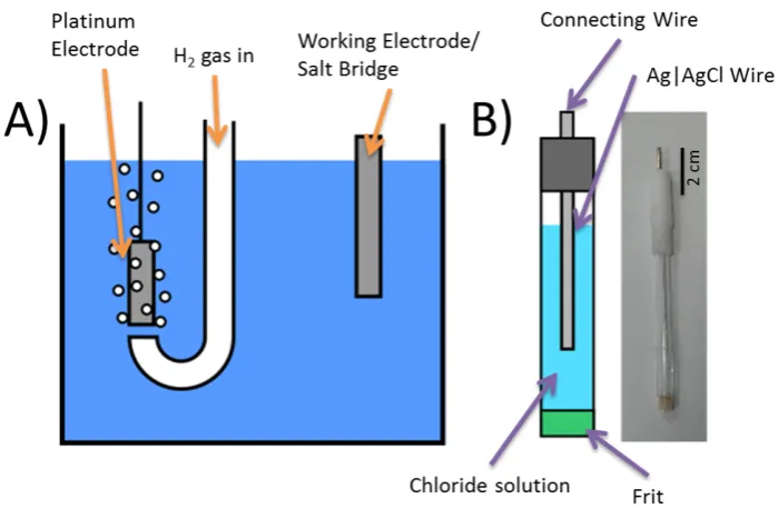
and is achieved physically by chlorodizing the outside of a silver wire then sealing the wire in a tube filled with Cl– saturated solution, such as KCl. There is a metal connector through the top of the tube so the electrode can be connected to a circuit and a frit at the bottom of the tube so current can be passed into the saturated solution from the bulk solution without contam-ination in either direction. (See Figure 1.1(B)) The electrode pictured is of a standard size, although they can be slightly smaller they are still large, bulky and fragile and not suitable for incorporation into scanning microscope probes or flow cells which restricts their usage to bulk measurements. When smaller, thinner electrodes are needed a quasi-reference counter electrodes (QRCE) can be used. These electrodes are reasonable stable, but do not have the constant equilibrium that reference electrodes do. They can be made from a thin metal wire often simply platinum or silver. To fabricate a QRCE similar to the Ag|AgCl electrode the same process is applied to chlorodize the silver wire, but then the wire is washed in water and used without being in contact with a saturated solution, directly into the solution of interest.1 If this contains a
reasonable Cl– concentration the potential is fixed.2
Figure 1.1: Schematic of both A) standard hydrogen electrode and B) Ag|AgCl electrode. Also shown in (B): a photo of a Ag|AgCl electrode.
A staple of electrochemical research is linear sweep and cyclic voltam-metry (LSV and CV). This is an experiment which sweeps the potential of either the working or reference electrode and the resulting change in current is measured, linear sweep voltammetry sweeps the voltage in just one direction. In the more commonly used cyclic voltammetry the potential is swept back and forth for any number of cycles. The uses of CV include, but aren’t limited to: observing the overpotential of redox reactions,3 reversibility of those re-actions,4 calculating charge density, observing capacitance,5,6 and ion current
rectification7 and various electrode cleaning procedures.8
1.2
Scanning Probe Microscopy
Scanning probe microscopy (SPM) is an umbrella term for any microscopy technique that employs a positionable, physical probe to collect data which can then be interpreted as a physical property of the surface, such as sample height, or chemical reactivity.9 SPMs have revolutionised how we study surfaces and
the probe collects is only a dependent variable of what is to be measured. Rather like the affect of aberrations and minimum wavelengths have on optical and electron microscopy, SPM must consider the morphology of the probe used and its potential affect on the data recorded.
1.2.1
Atomic Force Microscopy
Atomic force microscopy (AFM) is one of the older forms of SPM. This tech-nique came directly after scanning tunnelling microscopy (STM)10 and was
a breakthrough for imaging as AFM was capable of scanning non-conductive surfaces, unlike STM. First developed in the mid 1980s by Binniget al,11 the technique employs an extremely sharp tip, on the end of a horizontal can-tilever, which is brought into contact with a surface and then the movement of the cantilever bending against the surface can be used to map topography. The cantilever is reflective and a laser is aligned precisely onto the back in order to reflect onto a detector. When the tip is pulled onto a substrate, due to inter-atomic forces, the cantilever bends, as shown in Figure 1.2(A). The detector records the movement of the laser as the cantilever bends due to the topography of the sample that the tip is scanning. This deflection is converted to height and a topography map is recorded. The activity of inter-atomic forces can be seen in the force curves. A schematic of an approach and retract of an AFM tip to a surface is shown in Figure 1.2(B).
The generic shape of a force curve shows the tip coming into contact suddenly as the inter-atomic forces pull the tip down. The retract will not mimic the approach, as the tip can become stuck to the surface by atomic force, and the adhesion of the tip on the surface has to be overcome.
Figure 1.2: A) Schematic of the AFM tip as it makes contact with a surface, bends the cantilever and deflects the laser. B) Sketch of a force curve showing the approach (blue line) and retract (red line) of an AFM tip.
objects not sufficiently attached, the tip can damage the surface or drag objects on the surface around, for example polymer fibres unsecured to a surface.12
There is an alternative method called ‘tapping mode’ which alleviates these problems to a certain extent. In tapping mode the probe still makes physical contact with the surface but only intermittently. An oscillation is applied at or near the cantilever’s resonant frequency, and the amplitude is monitored. Many different tip sizes and shapes have been developed and the resonant frequencies range between 1 kHz to 1 MHz. When the tip nears the surface, the amplitude experiences dampening, which can be used as feedback to indicate the tip has reached the surface. Although this method has longer scan times than contact mode due to the slow movement of the tip towards and away from the sample, an advantage is that a force curve can be recorded at each point. Force curves can provide a large volume of different information on the physical properties of the sample.13 Figure 1.2(B) shows a generic force
curve, in reality the gradient of the attraction, and the height of the pull-off force and the distance from the surface at which these events take place can all be used to inform on a range of different surface properties. These include, but are not limited to, surface hardness,14,15 adhesion,16,17friction,18and elas-ticity.19
use as a characterisation technique. Efforts have been made to expand the functionality of AFM. Chemical sensitivity can be added to AFM experiments by chemically modifying the end of the tip.20 Conductive AFM (C-AFM)
employs a metal coated tip which, during a scan, passes a current between the tip and sample under an applied bias, so that a topography and conductivity map are recorded simultaneously.21 Studies on molecular wires have used
C-AFM to look at conductive molecules within nonconductive self-assembled monolayers (SAM).22 Crystal dissolution studies with direct relevance to the concerns of this thesis will be discussed in Section 1.4.3.
1.2.2
Scanning Electrochemical Microscopy
Scanning electrochemical microscopy (SECM) was first developed by Bard et al in the late 1980s.23 Employing an ultramicroelectrode (UME) as a probe
to investigate the electrochemistry of surfaces, and for the first time a scan-ning probe could be used to probe specific chemicals.24 To create microscale
electrodes two methods are predominately used. The first method is to etch a metal wire down to a conical tip and then insulate the wire excluding the end of the cone. A number of different coatings have been investigated in-cluding silica coatings and various polymers.25 Even sub-micron probes have been reported with this method.26 However, these conical probes proved not to have the desired level of reproducibility. The second method creates a disk electrode by starting with a wire of the diameter required for the finished elec-trode and sealing it in glass using a laser puller to stretch out a capillary.27
Standard sizes are tens of microns, commonly 25µm28,29but nano sized probes
have been created,30 with probes as small as
∼20 nm now being reported.31,32
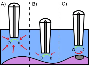
Figure 1.3: A) The UME in bulk, slowly turning over reactant. B) When approached to an insulating surface mass transport to the UME is decreased, and therefore a lower current is recorded at the UME. C) Approaching to a conductive surface will result in a higher current as the product of the reaction is renewed.
analysing data and when designing simulations to mimic an SECM system. Some applications of SECM include studying the hydrogen evolution reaction (HER) for use in fuel cells,33 patterning nanostructures,34 and probing fluxes
through materials such as human dentine,35 and nanopores.36 SECM has also
been used to study crystal dissolution, which will be discussed in Section 1.4.3.
Modes of Operation
Upon invention, the technique immediately presented a number of different scanning modes.37 The most simple is the feedback mode. As shown in
the UME is blocked and the recorded current at the UME will drop (Fig-ure 1.3(B)). Conversely, approaching to a conductive surface will increase the current, because the surface will regenerate the reactant (Figure 1.3(C)).
Another mode is known as tip generation - substrate collection (TG-SC).38,39 A steady, quantifiable stream of reactant is generated at the probe
and is collected at the substrate with up to 100% collection efficiency. This makes TG-SC excellent for experiments such as screening for oxygen reduction reaction catalysts,40 among many other applications. Microarrays of different alloys can be quickly fabricated and compared in a single experiment. Hy-drogen oxidation has been studied in much the same way on a selection of noble metal electrodes.41 In some cases it is the reaction at the surface itself
that is in question and so substrate generation-tip collection (SG-TC) can be used. SG-TC has been employed to study diffusion coefficients,42 and oxygen
reduction reaction mechanisms.43
Both of these techniques can be used only on conductive substrates, and they lack the ability to simultaneously measure topography. A solution to these problems is AC feedback mode. There are a variety of modes under the umbrella term ‘AC experiment’. They can be divided into two main categories: piezo oscillation and bias oscillation. In piezo oscillation mode, an AC signal is added to the physical movement of the probe, also known as ‘shear force’ mode, one piezo is oscillated and another measures the dampening of this oscillation as the probe reaches the surface.44,45 This mode requires new hardware so
signal.46,47 This mode has been used for a range of applications including
studying corrosion48 and imaging living cells.49,50
Combined Scanning Electrochemical Microscopy and Atomic Force Microscopy
To further enhance the capabilities of SECM, work has been done to couple UMEs with other probes, the most common are SICM, which will be discussed in Section 1.2.3, and AFM. The combination of AFM and SECM provides chemical sensitivity and excellent topography capability in a single probe.51,52
Tip creation began as a complicated process that made one probe at a time sealed in a polymer51 or glass.53 In more recent years advances in
microfabri-cation has allowed batches of tips to be produced, utilising focused ion beam (FIB) milling.54,55 Tips tend to be one of two forms: conductive apex or
re-cessed electrode. The former are created by modifying conventional AFM tips. The tip is coated with a conductive layer and then an insulating layer, with the conductive tip re-exposed from the insulating layer, either mechanically or using FIB. Tips have been fabricated from conductive materials such as platinum,56 boron doped diamond (BDD) or gold.57
Because AFM tips make physical contact with the surface there is a great risk that the electrode will be damaged during a scan, which may make conductive apex tips inherently fragile. Recessed electrode style tips were designed to avoid this problem by having the SECM electrode set back, slightly above the AFM tip. A number of fabrication methods exists including FIB milling an AFM tip onto the end of an epoxy covered UME,58or FIB etched out of BDD.59,60 This combined technique can be used for a great many different topics, from inorganic problems such as corrosion58,61 to answering biological questions about the activity of living cells.62,63
1.2.3
Scanning Ion Conductance Microscopy
From its inception64 to the present day scanning ion conductance microscopy
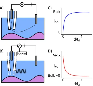
approached towards a surface of interest and, as the probe reaches approxi-mately 1 tip diameter away from the surface, the currents starts to decrease as the surface starts to obstruct the solution from entering to probe, which increases the resistance in the circuit. This drop in current is detected and is used as feedback to scan laterally across a surface to measure topography. This technique has also been used to measure the release of ions from a sub-strate containing pore features.65,66 A schematic diagram of the most basic SICM setup is shown in Figure 1.4(A). Relying solely on the DC ion current as a method of feedback can be unwise, as many factors can impact the DC current such as local or general changes in ionic strength, particulate matter blocking the pipette or drift of the current.67
For more reliable feedback the probe is oscillated in the Z direction. When close to the sample surface, the resulting AC current can be used as feedback. The AC magnitude is essentially the gradient of the DC-distance curve. Thus, in bulk solution there is no variation in DC current and the AC value will be minimal. The differences are shown in Figure 1.4(C and D) where C shows the DC current decreasing with height, while the gradient of that de-crease inde-creases so too does the magnitude of the AC current. Once the probe begins to reach the surface the DC current will change with the oscillating position of the probe. This will induce an AC current of the same frequency as the applied Z oscillation, which can be detected by a lockin amplifier (the function of which will be discussed further in Section 2.4.3).
As well as these two modes of approach, SICM also has two main modes of scanning. Constant distance mode, analogous to contact mode in AFM, rasters the probe close to the surface, at a constant separation, while the Z piezo moves to try and maintain a constant value for either DC or AC.68 Hop-ping mode, approaches the probe to a given setpoint then retracts the probe into the bulk before moving laterally and approaching the surface again.69
Applications of SICM
Figure 1.4: Schematic of SICM setup for both A) DC feedback and B) AC feedback. C) DC approach curve showing the drop in current as the probe approaches the surface, due to the surface restricting ion flow. D) AC approach curve increases as the DC current becomes dependent on height.
samples.70 This has led to a much greater understanding of cells in-vitro and has been used to image cells in a wide variety of projects, such as proteins in living cell membranes,71 cell volume measurement,72 and leaf surface mor-phology.73 An additional advantage is that the probe does not make physical
contact with the sample, unlike AFM that has been proven to deform cells as they are being scanned.73,74
Combined Scanning Electrochemical - Scanning Ion Conductance Microscopy
With a number of incredible high resolution techniques for measuring topog-raphy of both conductive and non-conductive substrates now available, a push has been made toward functional imaging. Maps of surfaces that can inform on surface properties and activity rather than just topography. SECM, as a stand alone technique, can achieve this, but at the expense of accurate topog-raphy. When the two techniques are combined into one dual-function probe, both topography and reactivity can be mapped simultaneously. SICM-SECM has a number of advantages over AFM-SECM, namely, probes can be based on glass capillaries making them cheap and easy to produce.
There are a number of ways to fabricate SECM-SICM probes, each with a different geometry. Starting with a regular SICM probe, an SECM electrode can be added to the side by evaporation of an electrode material such as gold.77 More commonly a dual-barrel pipette is used and an electrode is fabricated in the barrel for SECM by pumping butane gas down the wide end of the probe and heating the tip. The butane forms a carbon electrode at the tip of the SECM barrel.78,79 To prevent the SICM barrel becoming blocked with
carbon it is temporarily blocked from the wide end and an inert gas is pumped towards the tip end to prevent the butane from the SECM barrel escaping and ensuring it is burnt to form carbon. The downside of this technique is that the carbon can be recessed far back down the barrel and the exact distance of the recession is not reproducible. The best probes have to be flattened using FIB milling.80
Both SICM and SECM are non-contact techniques, which means the probes do not risk damaging the sample or becoming damaged themselves dur-ing regular use. Although SECM-SICM is a relativity new technique, studies have proven the techniques ability in SG-TC SECM mode,77 and it has been
used to investigate live cells81 and transport of species through pores and ion
1.2.4
Scanning Electrochemical Cell Microscopy
The technique of scanning electrochemical cell microscopy (SECCM) is very young but is finding many areas in which its abilities can be of considerable advantage. SECCM, like SICM, use cheap disposable probes created from glass or quartz capillaries pulled to a sharp tip in a commercial laser puller. However, SECCM uses capillaries with a vertical wall, known as the septum, down the middle. These are referred to as ‘theta capillaries’.
SECCM Setup
When theta capillaries are pulled in a laser puller, the septum is stretched and thinned as well, producing a sharp tip with two micro, or nano, scale barrels. (Figure 1.5(1)). Both barrels are then filled with an electrolyte solu-tion appropriate for a given applicasolu-tion (Figure 1.5(3)). This can be anything from aqueous solutions85 to organics and even ionic liquids86 and there can
be a different solution in each barrel.87 The solutions in both barrels meet at the tip of the probe and protrude from it in the form of a liquid meniscus, this meniscus forms a connection between the two barrels. A QRCE is then added to each barrel, the material of which can vary depending on the solution. However most commonly a Ag|AgCl wire can be used, (Figure 1.5(4)). When electrical contact is made to the QRCEs, an electrochemical cell is formed (Figure 1.5(6)). The ionic current of this micro cell is dependent on the most resistive section of the circuit, which for the SECCM setup is always the liquid meniscus connecting the barrels. The state of the meniscus can be elucidated from the ion current in the cell. For instance to land the SECCM probe on a surface, the probe is moved vertically downwards until the meniscus contacts the surface. A sudden increase in ion current results from the meniscus di-mensions expanding and the resistance in the meniscus dropping. This can be detected and the vertical movement stopped in response before the physical tip touches the surface. 3D scanning over conductive and non-conductive sur-faces is possible (Figure 1.5(7,10)).
using SECCM and most will have a similar setup.88,89 For experiments on
non-conductive samples, a simplified version may be used in which only one potential is required, applied directly to the QRCE in one barrel, and a current follower is connected to the other QRCE.
Among the advantages of SECCM is that the meniscus from the probe can be landed on a surface without the surface needing to be submerged in an electrolyte solution. The spatial resolution of the technique is dependent on both the size of the probe opening and the wetability of the surface. The more hydrophilic a surface, the more an aqueous meniscus will spread, for example. However, in general a rule of thumb is that the meniscus wetting area is of the order of the probe size.90,91Depending on application the tip of the probe can
be silanised on the outside,90 this ensures that when the tip is filled with
so-lution the meniscus does not leak onto the outside of the probe (Figure 1.5(2)).
Landing the probe can be achieved with DC current feedback only, but in many cases the sensitivity and variability of the DC current means that a more sophisticated mode of approach is required. The most common mode of SECCM is distance modulation (DM), working under the same principles as AC-SICM, in which the probe is oscillated in the Z direction (Figure 1.5(5)). While in air the AC component of the barrel current is close to zero and does not change (similar to SICM). Once the meniscus makes contact with the sample the physical Z oscillation causes the meniscus to squash and stretch, therefore causing the ionic resistance in the meniscus to change and this gives rise to a detectable AC signal. This method is highly reproducible and reli-able. In addition, the SECCM probe can be modelled with a high degree of detail in computer simulations.90 This allows data from most experiments to be matched to simulated values.
Application of SECCM
a given AC setpoint, representative of a fixed distance away from the surface. A redox mediator was present in the barrels so when the probe was over gold an electrochemical current was detected which did not interfere with the topography measurement as the redox current was orders of magnitude smaller than the ionic current. Then when the probe is over glass no electrochemical current is recorded. In this manner two maps were plotted: topography and electroactivity.
The high spacial resolution has been used to answer important ques-tions about heterogeneity in the surface electrochemistry. Highly orientated pyrolytic graphite (HOPG) has often been used as a model for other carbon based materials, such as graphene.92 From macroscopic measurements it was
believed that only the step edges were active and were responsible for the en-tire electrochemical activity of HOPG. With the SECCM the surface could be mapped with spacial resolution high enough to distinguish these features and the results showed the basal plane had near-reversible electron transfer kinetics.93 The same principle was later applied to multilayer graphene, which allowed the differences between basal and step edges to be seen, as well as the differences between areas of different numbers of layers.94
Another advantage of SECCM is the high mass transport in the menis-cus. Due to this it has been possible to probe nanoscale structures for their surface kinetics with redox mediators. The electrochemical reactivity of single walled carbon nanotubes (SWNT) has been studied,95and in conjunction with
a finite element method (FEM) model proved to be reasonably uniformly active along their entire length. Single particle resolution has been achieved with this system.96 Platinum nanoparticles can be grown on pristine SWNT template
and each can be scanned for both size and chemical reactivity. The particles can then be investigated with SEM to provide an even greater understanding of their morphology and therefore how the size and shape of individual parti-cles affects their reactivity.
The SECCM has already been used for patterning of various materi-als.87,97 Conductive wires with a diameter matching that of the probe can
con-ductive surface it can be grown out onto an insulating surface. 3D structures can be constructed by moving the probe vertically.97 Poly-L-Lysine (PLL)
patterns have been deposited in order to create a sample analogous to living cells.98
Impressively, one study used two different solution in the barrel to de-liver, in a predetermined pattern, three colours, and therefore create an im-age.87 DNA will adhere to positivity charged surfaces so streptavidin coated glass was used as a substrate. In single colour tests it was observed that flo-rescence material would only deposit from one barrel, the barrel of matching charge that would push the material out. By reversing the potential it was possible to flip the direction in which the material was deposited. Varying the driving force of the potential deposits different amounts of material, resulting in a graded colour. Two materials can be patterned simultaneously by chang-ing the sign of the applied potential to drive the chosen species out. Green was deposited from rhodamine green labelled DNA and red from alexa 647-labeled DNA. Yellow can also be seen in locations where both species were deposited. In this fashion entire pieces of artwork can then be copied.
In the previous year more advancements have been made to the tech-nique. In order to collect more information about a surface, SECCM is being used in hopping mode and a CV run at each hop. To run several scans at fixed potential is highly time consuming, and only gives a small voltage reso-lution. Running a CV at every hop means that each pixel will have a voltage resolution limited only by the chosen data collection rate (hardware limits will typically be higher, on the order of tens of microseconds). The clearest way to show this high volume of data is to create a movie where each frame is the entire map at a single voltage. This produces a movie with hundreds of frames, showing the entire map as the voltage is swept, making it easy to see the affect of surface heterogeneity on reactivity.
The work of Chenet al99 shows this technique applied to the study of
in the mapped region were correlated to their grain orientation by combining SECCM images with electron backscatter diffraction (EBSD) data.
1.3
Ionic Crystals and Crystal Dissolution
Crystals, at their most basic, can be described as a solid composed of a regular, repeating arrangement of atoms or molecules. The study of crystal dissolu-tion is of high importance in many areas of nature science, such as geology and the carbon cycle,100,101 but also has huge importance in industries af-fecting peoples everyday lives such as in oral drug delivery102,103 to food104
and construction.105 Consequently, methods for studying crystal dissolution
are equally important, with a need for reliable techniques that can provide quantitative information on the kinetics and mechanisms.
1.3.1
Mechanisms for Crystal Dissolution
Dissolution is governed by two competing processes, mass transport and sur-face phenomena,106 as shown in Figure 1.6. These processes occur in series
so, when measuring dissolution rates, only the rate limiting step, the slower of the two, can be observed. The former is the movement of material from the interfacial region to the bulk solution, this occurs in three separate ways:
1. Convection, very generally, is defined as the physical movement of a fluid. This can be from natural causes, such as temperature gradients or density differences resulting from a reaction. Examples of artifcial introduced convection include the movement of solution under a mechanical force, such as stirring, or a flow cell. Convection can be purposefully added in the form of a rotating disk or flow cell in order to overwhelm the contribution from natural convection with a highly controlled and defined form, Increasing convection is also used to increase the overall mass transport rate, in order to access surface kinetics of some crystal systems. However, convection is usually discounted from experiments by keeping the solution still and at constant temperature or conducting each experiment on a short time scale.
as a function of diffusional flux (j), defined as the moles of material diffusing through a unit area in one second, this is Fick’s first law of diffusion.
j =−DB δ[B]
δx (1.3)
where [B] is the concentration of diffusing species B and DB is the diffusion
coefficient for B. Each species has a constant diffusion coefficient. A more useful form of this equation gives the change of concentration of B at a point in space. This is Fick’s second law and is used to describe the diffusion component in the time dependent 3D FEM models used in this thesis.107
∂[B]
∂t =DB
∂2[B]
∂x2
(1.4)
Diffusion is highly important to understand and quantify as it cannot be re-moved under experimental conditions.
3. Migration, which is movement of ions under an applied potential, is worth discussion here despite most crystal dissolution studies not requiring a potential to be applied. However, some techniques, such as channel flow cells and SECM are dependent upon the use of electrodes for detection or control and therefore migration must be considered. In this thesis, crystal dissolution is not dependent on an electrochemical reaction, however, an electric field is still present and is described as migratory flux, jm
jm ∝ −u[B] ∂φ
∂x (1.5)
where φ is the applied potential and u is the ion mobility.108 Ion mobility is dependent not only on the characteristics of the ion but also on the solution. H+moving in aqueous solution has a mobility of 3.62×10⁻⁷m2s−1V−1 at 298 K,109 and can move under the Grotthuss mechanism, in which rather than
a single pacticle moving, a proton will attach to a water molecule and force another off, then that one forces a proton from a second water molecule in a ’bucket chain’ style.110 However, most ions have a mobility on the order of
10−8.111 Migration carries the ion current through the bulk solution, however,
elec-Figure 1.6: Diagram of mass transport processes: A) Migration, particles moving under the influence of an electric field B) Diffusion, particles moving down a concentration gradient C) Convection, particles moving under the influence of an external force, in this case stirring. D) Surface processes: surface diffusion and adsorption/desorption.
tron transfer. In the large majority of cases migration can be neglected by increasing the ionic strength of the solution used.
Surface phenomena includes processes such as surface diffusion and the detachment of ions or molecules at the crystal surface, this detachment or movement of ions on a surface is often treated as following the terrace ledge kink model112. This model provides the basis to consider the processes of
adatoms desorbing, surface vacancies forming and step edges retreating. The relative thermodynamic probability of each of these processes will then vary between crystal systems.
[image:40.595.149.494.102.376.2]the kinetics of the surface processes to be measured. Additionally, due to the dependence of surface process rates on the surface morphology, different sites on the same crystal surface may have different dissolution characteristics.113
This means the most informative studies are those which have a means of controlling and defining the surface in question.
1.3.2
Defects in Crystal Structure
There is a considerable body of work on the topic of dissolution from dis-locations and defects, which can seriously alter and also control dissolution in crystals.114 Many types of defect exist, such as point defects, dislocations, stacking faults and grain boundaries.115,116 Point defects are single atom de-fects arising from breaks in a crystalline materials crystal structure, such as a missing atom or the wrong atom. Dislocations and stacking faults are more substantial defects which cause large section of a crystal to shift away from the crystalline structure. Grain boundaries tend to be formed when the many faces of the crystal are crystallising at the same time, when the faces grow towards each other they form a rough edge where they meet. A full awareness of the affect of defects in crystal structures is vital to understanding more complex dissolution kinetics as dissolution can partly or almost entirely dependent on defect density.117,118
1.4
Previous Techniques for Studying
Crystal Dissolution
Due to the range and variety of crystalline materials, a number of different methods for studying their dissolution have been required throughout the his-tory of the field. The earliest methods were fairly simple, batch techniques, where a sample was placed into an appropriate solution and the reaction fol-lowed by removing and analysing aliquots.119 These were easy to implement but unreliable. Once mass transport was better understood, hydrodynamic methods were introduced, which controlled mass transport allowing much more accurate and informative studies to be conducted.120 In more recent years,
of microscale sections of a crystal to be measured rather than an average of the whole surface that previous techniques were restricted to.
1.4.1
Batch Technique
One of the first methods for studying crystal dissolution utilised a batch setup in which powdered samples were dissolved in solution under controlled con-ditions.123,124 This normally consisted of a beaker filled with an appropriate
solution for the dissolution of the chosen crystal with a sample of crushed crys-tal powder. This powder is either recompressed into a disc or added in powder form to the solution. Dissolution rates were quantified by tracking the change of speciation in solution by taking aliquots and employing a complementary technique. The dissolution rates measured using this technique are averaged over all crystal faces exposed to the solution. This setup can be stirred but convection is usually complex and ill-defined.
1.4.2
Hydrodynamic Control Techniques
The next generation of crystal dissolution techniques introduced the ability to control the hydrodynamics of the studied systems. The first technique in this category is the rotating disc (RD) method. Based on the rotating disc elec-trode125, this method used well-defined hydrodynamics to control and increase
mass transport. A disc of the crystal to be studied, either made by compress-ing powdered crystal126 or by mechanical cutting of a single crystal127, is rotated in an undersaturated solution, the exact level of undersaturation and other factors such as pH128 and temperature128,129 can be chosen. The solu-tion composisolu-tion can then be monitored with respect to time as dissolusolu-tion occurs, the method to measure this change normally consists of taking aliquots of the solution while dissolution is occurring and testing the composition for the concentration of the crystal being dissolved.130Higher mass transport rates
limit to how fast you can rotate a sample, this physical limit means that there is a maximum rate that mass transport can reach and systems with a higher surface kinetics than this can not be probed.
An alternative to RD was the Channel Flow Cell (CFC) methods in which the etching solution is flowed under laminar conditions through a flow cell which provides a well-defined hydrodynamics at the substrate surface.134,135 Aliquots are removed from downstream of the flow cell and their composition can be measured with respect to time with a range of quantitative analyt-ical techniques, i.e. Raman spectroscopy,136 interferometry129 or mass spec-troscopy.137Real time monitoring can be performed by positioning an electrode
downstream of the crystal to measure the rate of dissolution by electrochemi-cally detecting the concentration of dissolved product.138
Limitations exist for these systems however, even if higher dissolution rates are accessible, for some systems the higher mass transport is still not high enough to enter a surface controlled system.139 Flow rate and rotation speed can only be increased up to a point before reaching physical limitations. Another drawback is the sample preparation restrictions. These techniques require large flat bulk surfaces127,140 or samples embedded in a support mate-rial.134 No microscale analyse is possible as these techniques can only give a
dissolution rate that is an average for the whole surface.
1.4.3
Scanning Probe Techniques
A different approach to dissolution measurements involves using scanning probe microscopy techniques to allow real time monitoring of crystal disso-lution and eliminate a number of drawbacks the previous techniques were hin-dered by. Unlike the previous techniques, SPM can provide spatial resolution of crystal dissolution allowing the study of heterogeneities across the surface. Measurements are no longer limited to an average of the entire sample sur-face. Such techniques include in-situ atomic force microscopy (AFM),141,142 and scanning electrochemical microscopy (SECM).45,143 In-situ AFM has been
used to track the movement of step edges along a crystal surface,144 with the
followed on a series of images,145,146 this speed reaches 20-50 nm s−1. A wide
range of materials have been studied, some include calcium based minerals such as dolomite, calcite147,148 and gypsum149 and weak acid compounds such
as aspirin102 and oxalate.150 However, the use of AFM to measure reaction
kinetics showed to be problematic; the probe has an impact on the hydrody-namics in the flow cell used during AFM experiments151 as well as the tip
having a wearing effect on the crystal surface.152,153 This can introduce errors in the dissolution rate measured. Moreover, many works in the literature re-port a big discrepancy between dissolution rates measured via AFM and other techniques for the same material showing a difference between microscale and bulk measurements.154
SECM can be used to study crystal dissolution, the probe is positioned close to the surface of the sample to probe or trigger dissolution.112 The probe
can promote dissolution by generating a species that is reactive with the sub-strate e.g. H+ for enamel143 or calcite155 etching. The work of McGeouch
et al143 looks at the dissolution of calcium hydroxyapatite (HAP), the major component of enamel. HAP is amenable to SECM study as it dissolves via acid attack following the equation:
Ca10(PO4)6(OH)2+ 8 H+10Ca2+(aq)+ 6 HPO−24(aq)+ 2 H2O (1.6)
To avoid the problem of having to generate protons and recordin-situ the re-sulting products, this study used the UME to quantitatively produce protons next to the surface of enamel and then study the etch pits ex-situ using in-terferometry. The parameters of the physical experiment were used to inform a novel moving boundary finite element method (FEM) model and rate infor-mation could be deduced. The simulated value for heterogeneous dissolution rate was found to be 0.08±0.04 cm s−1.
be reduced to release Cl– locally by the UME, following the reaction:
Cl3CCOO−+ H2OCl2CHCOO−+ OH−+ Cl− (1.7)
The work of Seo et al157,158 also studied the corrosion of iron but using a Ag UME coated in AgCl to deliver Cl– to the surface. The probe was approached to the iron surface and the reaction shown in Equation (1.2) can be driven to the left hand side to generate Cl– ions to dissolve the iron. A passive film was formed on the iron prior to dissolution and SECM was shown to detect the different products of passive layer and iron corrosion. SECM dissolution techniques can be used only with crystals which are stable in a bulk solution and their dissolution must be triggered electrochemically, e.g. pH change143
or susceptibility to a certain ion, such as Cl– on iron.156 This high spatial
resolution gives SECM the ability to make multiple measurements on a single sample.159A major drawback of this technique is that it requires the sample to be submerged in a bulk solution. There is also a lack of any feedback system to measure topography.
1.5
Surface Charge and the Electric Double
Layer
Surfaces and particles often exist with an intrinsic surface charge, the nature of which arises from the terminal groups on the edges of the substance. For example, glass is an insulator but still has a surface charge due to the hydroxyl groups at the surface. In contact with a solution, the hydrogen can dissociate leaving a negative charge on the remaining oxygen atom. The charge on the surface will be compensated for in the solution by the creation of a layer of counter ions, this simplistic view of two layers of opposite charge gives rise to the name ‘electric double layer’ (EDL).
Figure 1.7: A) The Helmholtz model of point charges on an oppositely charged solid surface. Superimposed on the diagram is a sketch of the potential drop from surface potential, φs to the bulk potential φb. B) Gouy-Chapman model
that represents the double layer as a continual and diffuse layer.
be defined as the surface charge on a solid surface and the opposite charge extending into a salt solution in contact with that solid.
This phenomenon was first proposed by Hermann von Helmholtz whose theory stated that surfaces in contact with a solution can build up charge like a capacitor. The Helmholtz model treated the counter ions as fixed to the surface of the solid in a ‘compact layer’.160 At the surface of the electrode the
to the surface. In the early 1910s, both Gouy and Chapman independently developed the Helmholtz model to consider the influence of both the charge of the solid and concentration in the solution. Instead of a single compact layer of adsorbed solvated ions, the EDL was described as a ‘diffuse double layer’ (DDL) where the ions are mobile due to Brownian motion and the length of the double layer varied with concentration. The potential charge extends out into the bulk whilst dropping exponentially in magnitude, as shown in Figure 1.7(B). The lower the concentration the further into the solution the DDL reaches, with less ions in solution the double layer must extend further in order to equilibrate the charge on the surface. The limits of this model are seen at high bulk concentration when ions, treated as point charges, have no maximum concentration close to the surface.161Despite this limitation for high
concentrations, at low concentrations the Gouy-Chapman model is a good ap-proximation and will be used in this thesis as the basis for calculating surface charge as all experiments will be conducted in solutions of low ionic concen-tration.
The model was developed further by Stern (Figure 1.8(A)) to have aspects of both the compact layer consisting of solvated ions close to the elec-trode and also the DDL.162 This was an important step as it fixed a problem
with the Gouy-Chapman model by accounting for the finite size of the ions and the minimum distance they can be from the surface. Grahame was then the first to outline a theory including the specific adsorption, which gave the double layer three distinct regions.163 The first layer in this model is the inner
Helmholtz layer (IHP), which accounts for specific adsorption of ions on an electrode surface. These ions have no solvation shell, and could be co-ions or counter-ions, and as such this will only occur for certain ions. For instance, it has been shown with electrocapilarity measurements on a mercury electrode that positive ions are highly unlikely to lose their hydration shell, whereas negative ions can adsorb to the surface.164
Model (BDM),165 takes account of the fact that the solvent molecule is
[image:48.595.146.507.244.522.2]al-ways the highest concentration of any species at the interface, as reflected in the representation shown in Figure 1.8(B). Common to all the models is that the majority of potential drop occurs close to the electrode, in all but the Gouy-Chapman model this is due to the presents of the compact layer. The BDM model predicts the potential drops with a higher gradient between the electrode and the IHP.161
Figure 1.8: A) The double layer model developed by Stern which incorporates the ideas of both Helmholtz and Gouy-Chapman. B) The BDM model show-ing the abundance of solvent molecules at the surface and the three distinct regions: IHP, OHP and diffuse layer. Superimposed on both diagrams are sketches of the potential drop from surface potential, φs to the bulk potential φb
1.5.1
Current Methods for Probing Surface Charge
electrocapillar-ity curves from a glass capillary filled with mercury. The capillary is held in a bath of aqueous solution and has a mercury reservoir at the top, the potential between the mercury and aqueous solutions can be changed, which, in turn will change the surface tension. These measurements allowed surface tension
vs potential to be plotted, thus by knowing the surface tension, a value for sur-face charge can be calculated. Unfortunately, this technique is applicable only to mercury, and due to its difficulty to implement and its toxicity, mercury is no longer commonly used as an electrode in electrochemical experiments. This technique presents no possibility of being used for non-conductive samples.
The surface charge on colloids is an important factor when designing them to resist coagulation, thus a range of techniques emerged to study what is known as the zeta potential of the particles.166 The zeta potential is
theo-retically similar to the electric potential in the double layer, as the colloidal particles are dispersed in an ionic solution there exists a double layer, how-ever the zeta potential is defined as a different point out into the bulk than either helmholtz planes. Electrokinetics167 and electrophoresis168 have been used to measure the zeta potential but are both based on the movement of colloids in an electric field. Because of this, only particulate matter can be measured rather than solid surfaces, and only an average of all particles is obtained. There is the possibility of using probing particles to measure the zeta potential of a surface, which has been demonstrated with new hardware (Desla Nano,Beckman Coulter).
An adaptation of AFM has been used for surface charge measurements, it has been shown that the force curve towards a surface is a function of the surface charge,169 and the AFM setup is already capable of imaging on conductive and non-conductive surfaces. However, the tips needed to achieve this functionality are highly specialised. The method to fabricate reproducible tips is labour intensive and non-trivial.170In addition to this, all the drawbacks
layer, none of them provide a robust and versatile platform for non-contact mapping of surface charge on a substrate.
1.5.2
Surface Charge Mapping
This thesis will introduce the concept of using SICM as a robust and simple technique for surface charge mapping. This introduces the ability to map functional surfaces, the spatial resolution of which is increasing as methods for fabricating nano-sized glass tips become more reliable, probes down to
<50 nm radius have been reported.171–173 However, to fully appreciate the
data collected from these sub 100 nm probes, current rectification must be accounted for as it can be seen on glass pipettes174 and nanopores7,175 of this size regime. The double layer is a function of solution composition and surface charge therefore by knowing the precise solution composition and measuring the double layer a reliable value for surface charge is definable. Based on the Gouy-Chapman model the thickness of the double layer can be expressed as the inverse thickness of the double layer (κ cm−1) defined as
κ∝εzpCb (1.8)
whereεis the dielectric constant, z is the charge of the ionic species and Cb is
the concentration of ions in bulk solution. The variableκrepresents the inverse of a characteristic thickness of the double layer at a given concentration and surface potential. To predict the double layer potential to its full extent into the solution the following equation can be used,
φ=φbeκx (1.9)
where φ and φb are the applied potential at the surface and bulk potential,
respectively, and x is the distance from the surface. These equations are based on reasonable assumptions but do not provide accurate values for surface charge. The problem is challenging as surface charge on a substrate can be highly heterogeneous.
repro-ducibility, and the technique can be used with a wide range of samples and solutions. In order to observe surface charge, the double layer on the surface must be comparable in size to the diameter of the SICM probe, which in 10 mM salt solution, not only is possible, but also reproducible. The ability to map surface charge on the nanoscale will allow new research into tailoring how electrodes work under extreme or non-ideal conditions, how drugs interact with different cells or how to design functional polymers for better performance in a range of tasks, such as shampoo or colloidal paint and electrospray deposited paint.
1.6
Aims of this Thesis
Scanning probe microscopy techniques have a long history and an ever widen-ing range of capabilities; the possibilities for functionality, speed and resolu-tion are great. Improving SPM techniques is also of high importance because surfaces and structures need to be studied on the nano scale in order to be properly understood. It is one accomplishment to study a new system with existing techniques but another accomplishment altogether to design and build a technique better suited to studying emerging problems. This is why the next two chapters of this thesis are concerned with the methods and techniques em-ployed. The second chapter not only outlines general experimental information but also gives a detailed description of the experimental setup, explaining the hardware and its uses. The third chapter deals with the software used to run the microscopes. An in-house LabVIEW codebase is described in this chap-ter. The main design point of the codebase is that only one version would be needed for any of the nine rigs that are available in the Warwick group. The codebase is flexible enough to accommodate variation in the hardware used for each microscope and also functional enough to allow for a wide range of experiments with different types of scanning probe.
to measure the surface charge of a dissolving crystal will be highly beneficial to our understanding of the process. The forth and fifth chapters look at using the SECCM setup for the study of NaCl and calcite dissolution. The NaCl study introduces the dual-barrelled conductance micropipette for studying dis-solution with high time and spatial redis-solution. The fifth chapter is based on the same technique but this time combines the dual-barrel pipette technique with AFM. Using two different techniques that compliment each other is very powerful and provides more information about the system. Both these studies were completed with the addition of a FEM model designed to quantitatively deduce the dissolution rate constant in both systems.
Chapter 2
Experimental Methods and
Instrumentation
“We are stuck with technology when what we really want is just
stuff that works.”
Douglas Adams
2.1
General Materials
Minisart Syringe Filters) as the diameter of the SICM probes are of a similar order to dust particles in the solution, which could cause the probe to become blocked. The solution for mercury electrode experiments was degased with BOC Pureshield Argon and had a supply of argon blowing over the solution during the experiment. A list of all other materials and chemicals can be found in Table 2.1
Table 2.1: List of all chemicals and materials used in this thesis.
Name Details Source
(3-aminopropyl)triethoxysilane 98% Sigma Aldrich 11-dodecanethiol 98% Aldrich
11-mercaptoundecanoic acid 95% Aldrich
Acetone 99% Sigma Aldrich
Alumina na Buehler
Chloroform 99% Fisher
Dimethyldichlorosilane 95% Sigma Aldrich Hydrochloric acid 37% VWR Chemicals Isopropylalcohol Reagent grade VWR Chemicals Mercury(I) nitrate dihydrate 97% Sigma Aldrich Nitric acid 62-66% Sigma Aldrich Perchloric acid 70% Acros
Platinum wire 25µm Goodfellow Poly-L-lysine Mw 30k-70k Sigma Aldrich Polystyrene Mw 280k Sigma Aldrich Potasium chloride 99% Fisher
Potasium nitrate 99% Sigma Aldrich Silver wire 0.125 mm Goodfellow Silver wire 0.25 mm MaTecK Sodium chloride 99.92% Fisher Toluene Reagent grade Fisher