warwick.ac.uk/lib-publications
A Thesis Submitted for the Degree of PhD at the University of Warwick
Permanent WRAP URL:
http://wrap.warwick.ac.uk/89938
Copyright and reuse:
This thesis is made available online and is protected by original copyright. Please scroll down to view the document itself.
Please refer to the repository record for this item for information to help you to cite it. Our policy information is available from the repository home page.
2
Strain relaxation study of
Si
1−x
Ge
x
& Ge
buffer layers on Si(001) and InSb on
Ge/Si(001) virtual substrates
by
Vineet Sivadasan
Thesis
Submitted to the University of Warwick
in partial fulfilment of the requirements
for admission to the degree of
Doctor of Philosophy
Department of Physics
3
Declaration
This thesis is submitted to the University of Warwick in support of my application for
4
Abstract
Due to their direct and tuneable bandgap, III-V semiconductors offer variations in
electrical properties, compared to silicon. However wafers of III-V materials are more
expensive to manufacture and have higher defect densities than Si(001). Epitaxially
depositing high quality thin films of III-V materials onto Si(001) substrates offers a
more cost effective route to manufacturing state of the art III-V electronic devices,
whilst mitigating defect generation through lattice and thermal expansion coefficient
mismatches.
In this study, pure Ge and Si1−xGex layers are deposited as thin film heterostructures
on on-axis and 6° off-axis Si(001) substrates using reduced pressure chemical vapour
deposition to act as strain tuned “buffer layers” to integrate a particular III-V
compound onto the substrate. The films are characterised using transmission electron
microscopy (TEM), atomic force microscopy (AFM), high resolution X-ray diffraction
(HR-XRD) and defect etching & differential interference contrast (DIC) optical
microscopy.
The first key finding in this study relates to the development of an 78nm Ge buffer
which is comprised of a LT seed layer followed by controlled annealing only and at a
fraction of the tensile strain of state of the art thick LT/HT Ge buffer layers. The second
key finding comes from the comparisons between the established linear Si1−xGex
grading (LG) process with the recently developed reverse linear Si1−xGex/Ge grading
(RLG) process. Continuous tensile strain relaxation in RLG even up to x=0.45 yields high quality buffer layers with ≤ 3.7nm roughness, × 107cm−2 TDD and consistently
delivering 0.2% tensile strain albeit with a rise in stacking faults past 70% Ge.
The third major discovery comes when omitting the reverse graded layer entirely in
the RLG structure and depositing a constant composition Si1−xGex step on the Ge
buffer layer. High misfit dislocation densities and surface roughening is observed
leading to the formation of Kirkendall voids in the Ge underlayer as a strain relieving
5
The final chapter of this study investigates solid source molecular beam epitaxy growth
of high quality indium antimonide which has the highest lattice mismatch of any
III-V compound to Si(001) at 19.3% using the highest quality pure Ge buffer layers on 6°
off-axis Si(001). HR-XRD reciprocal space maps shows identical levels of strain in
Ge buffer layers grown on on-axis and 6° off-axis substrates, however an increased
degree of tilt is measured in the off-axis Ge buffer layer, with reduced degree of tilt in
6
Publications and conference presentations
Refereed Publications
1) V. Sivadasan, M. Myronov, S.D. Rhead, V.A. Shah, D.R. Leadley,
“Comparison of 𝑆𝑖1−𝑥𝐺𝑒𝑥 relaxed buffer layers grown on Si(001) substrate by
linear grading and reverse linear grading approaches” (in preparation for
submission 2016)
2) V. Sivadasan, M. Myronov, S.D. Rhead, “Ultra-thin Ge buffer layers on
Si(001)” (in preparation for submission 2016)
3) V. Sivadasan, M. Myronov,S.D. Rhead, “Kirkendall void formation in reverse
step graded 𝑆𝑖1−𝑥𝐺𝑒𝑥/𝐺𝑒 buffer layers on Si(001)” (in preparation for
submission 2016)
4) V. Sivadasan, M. Myronov, S.D. Rhead, J.E. Halpin, D.R. Leadley, “Tilt
comparison in reverse terrace graded and reverse linearly graded
𝑆𝑖1−𝑥𝐺𝑒𝑥/𝐺𝑒/𝑆𝑖(001) virtual substrates” (in preparation for submission
2016)
5) V. Sivadasan,M. Ashwin,G. Colston, S.D. Rhead, M. Myronov, “High quality
InSb epilayers grown on AlSb/Ge/Si(001) virtual substrates for photonic and
7
Conference Presentations
V. Sivadasan, M. Myronov (presenter), S.D. Rhead, V.A. Shah, D.R. Leadley, “Comparison of SiGe relaxed buffer layers grown on Si(001) substrate by forward and reverse Ge grading approaches” EMRS 2014 Spring Meeting, Lille, France, May
26-30, 2014.
V. Sivadasan (presenter), M. Myronov,S.D. Rhead, J.E. Halpin, D.R. Leadley “Reverse terrace graded 𝑆𝑖1−𝑥𝐺𝑒𝑥/𝐺𝑒/𝑆𝑖(001) virtual substrates grown using
8
Table of Contents
User’s Declaration……….1
Title page ... 2
Declaration ... 3
Abstract ... 4
Publications and conference presentations... 6
List of figures and tables ... 13
Acknowledgments ... 36
1. Introduction ... 38
1.1. Silicon electronics and the semiconductor industry. ... 38
1.2. Motivation behind developing Si1-xGex and Ge buffer layers on Si(001) ... 39
1.2.1. III-V materials integration onto Si(001) ... 39
1.2.1.1. III-V photovoltaics. ... 40
1.2.1.2. III-V Optoelectronics and photonics. ... 41
1.2.2. Strain engineered epilayers for CMOS and spintronic applications ... 42
1.3. Scope of work ... 42
2. Theoretical Discussion. ... 44
2.1. Semiconductor crystallography. ... 44
2.2. The Reciprocal lattice. ... 47
2.2.1. Bragg diffraction in crystals ... 48
2.3. Material properties of group IV and III-V semiconductors... 49
2.3.1. Properties of silicon, germanium and Si1-xGex alloys. ... 49
2.3.1.1. Material properties of silicon, germanium and Si1-xGex alloys. ... 49
2.3.1.1.1. Coefficient of thermal expansion ... 54
2.3.2. Properties of III-V semiconductors. ... 55
2.4. Epitaxy. ... 58
2.4.1. Reduced Pressure Chemical Vapour Deposition (RP-CVD). ... 59
2.4.1.1. Si, Ge and SiGe reaction kinetics using RP-CVD ... 61
2.4.1.1.1. Growth conditions for Si1-xGex epilayers... 65
2.4.2. Solid Source Molecular Beam Epitaxy (SS-MBE). ... 69
2.4.3. Adatom transport on the substrate surface and dimer bond energies ... 70
2.4.3.1. Growth on offcut substrates ... 72
2.4.4. Epitaxial growth modes ... 79
2.5. Strain relaxation and the formation of defects in FCC diamond and zinc blende epilayers. ... 81
2.5.1. Definitions of Strain and relaxation ... 81
2.5.2. Surface roughening ... 84
2.5.3. Defects. ... 85
9
2.5.5. Threading dislocations ... 89
2.5.6. Dislocation Mechanics ... 89
2.5.7. Nucleation and multiplication of dislocations. ... 91
2.5.8. Critical thickness of layer relaxation ... 93
2.5.8.1. Matthews-Blakeslee model ... 93
2.5.8.2. Nucleation of dislocations in a defect free substrate ... 94
2.5.8.3. Kinetic effects and interaction between dislocations ... 95
2.5.8.4. Dislocation pile-up and annihilation. ... 96
2.5.9. Stacking faults. ... 97
2.5.10. Crystallographic tilt ... 100
2.6. Cracks ... 102
3. Experimental Techniques. ... 103
3.1. Transmission Electron Microscopy (TEM). ... 103
3.1.1. Fundamentals of TEM. ... 104
3.1.2. Sample preparation. ... 107
3.1.3. Diffraction contrast TEM. ... 110
3.1.3.1. Two beam diffraction condition ... 112
3.2. High Resolution X-Ray Diffraction (HR-XRD). ... 115
3.2.1. Fundamentals of high resolution X-ray diffractometery ... 115
3.2.2. Reciprocal space and the Ewald’s sphere ... 117
3.2.3. Structure factor and conditions to meet Bragg’s law ... 118
3.2.4. ω-2θ coupled scans and reciprocal spacing mapping ... 120
3.2.5. RSM measurements on off-axis substrates. ... 123
3.3. Atomic Force Microscopy (AFM)... 125
3.3.1. Principles of AFM ... 125
3.3.2. Scanning modes: ... 127
3.3.2.1. Contact mode ... 127
3.3.2.2. Tapping mode... 128
3.3.3. Image analysis ... 129
3.4. Differential Interference Contrast (DIC) Optical Microscopy ... 130
3.5. Selective Defect Etching. ... 132
3.5.1. Dilute Schimmel etchant. ... 133
3.5.1.1. Etch rate comparison technique ... 134
4. Low temperature (LT) epitaxy of ultra-thin pure Ge buffer layers on Si(001) using RP-CVD. ... 136
4.1. Background on pure Ge buffer layers. ... 136
4.1.1. Development of the LT/HT Ge buffer layer ... 136
10
4.2.1. Thin LT Ge Buffer design ... 140
4.2.2. List of samples: ... 141
4.2.3. X-TEM comparisons of Ge buffer films grown at 400°C, 350°C and 300°C. ... 142
4.2.3.1. Growth rate and stagnation time ... 148
4.2.4. Annealing effects on thin Ge buffer layers. ... 149
4.2.5. Surface roughness of LT-Ge buffer layers ... 153
4.2.5.1. Surface roughness variation as a function of growth temperature: 300°C, 350°C, 400°C. ... 153
4.2.5.2. Annealing effects on LT-Ge buffer layer surface morphology ... 157
4.2.5.3. LT-Ge Surface morphology summary plots ... 159
4.2.6. Temperature dependent strain variation in the buffer layers. ... 161
4.2.7. Defect analysis ... 165
4.3. Chapter 4: Summary ... 172
5. Graded Si1-xGex buffer layers on Si(001). ... 173
5.1. Background to Si1-xGex buffer layers on Si(001) ... 173
5.1.1. Constant composition Si1-xGex ... 174
5.1.2. Step graded Si1-xGex/Si1-y/Gey ... 174
5.1.3. Linearly graded Si1-xGex ... 175
5.1.4. Reverse graded Si1-xGex ... 176
Reverse linearly graded Si1-xGex/Ge ... 177
5.2. This study on Si1-xGexgraded buffer layers using RP-CVD ... 178
5.3. Linearly graded Si1-xGex buffer design... 179
5.3.1. Buffer quality, surface morphology, strain and defect comparison at different grading rates and Ge% ... 181
5.4. Reverse linearly graded Si1-xGex/Ge buffer design. ... 189
5.4.1. Low temperature/ High temperature Ge underlayer. ... 191
5.4.2. Reverse linearly graded Si1-xGex/Ge buffer layers. ... 192
5.4.2.1. Morphology ... 196
5.4.2.2. Tilt and strain in Si1-xGex/Ge buffer layers ... 197
5.4.2.3. Defects... 199
5.5. Comparisons between linear grading with reverse linear grading ... 202
5.5.1. Strain comparison between buffer grading techniques: ... 202
5.5.2. Surface morphology ... 204
5.5.3. Defect comparison ... 206
5.5.4. Growth rate and etch rate variations ... 208
5.5.5. Crack generation ... 211
5.6. Reverse step graded Si1-xGex/Ge buffer design ... 214
5.6.1. Buffer quality variation with reducing Ge content in the Si1-xGex step. . 216
11
5.6.2. Reverse step graded (RSG) Si1-xGex/Ge structures. ... 219
5.6.2.1. Sample 15-73: RSG Si0.1Ge0.9/Ge buffer layer ... 219
5.6.2.2. Sample 15-77: RSG Si0.16Ge0.84/Ge buffer layer ... 221
5.6.2.3. Sample 15-74: RSG Si0.28Ge0.72/Ge buffer layer ... 223
5.6.2.4. Sample 15-75: RSG Si0.45Ge0.55/Ge buffer layer ... 227
5.6.3. Strain, surface morphology and TDD variation in RSG Si1-xGex/Ge buffer layers ... 230
5.6.3.1. Strain variation ... 230
5.6.3.2. Surface morphology variation ... 232
5.6.3.3. TDD variation ... 232
5.7. Chapter 5: Summary ... 233
5.7.1. Pros and cons of using linear and reverse linear graded Si1-xGex layers for III-V integration and strained channel devices ... 233
5.7.2. Reverse step grading and the formation of Kirkendall voids ... 237
6. Ge and Si1-xGex/Ge buffer layers on 6° off axis Si(001) substrates using RP-CVD. ... 238
6.1. Background to pure Ge buffer layers on 6° off-axis Si(001) substrates. .. 238
6.2. Background on terrace grading in Si1-xGex buffer layers ... 239
6.3. This study on Ge buffer layers on 6° off-axis Si(001). ... 240
6.3.1. Ge buffer layer on 6° off-axis Si(001) design. ... 241
6.3.2. Material quality of the layer through the stages. ... 242
6.3.2.1. Stage 1. Sample 15-172: LT-Ge buffer layer on 6° off-axis Si(001) ... 242
6.3.2.2. Stage 2. Sample 15-170: Anneal/HT-Ge/LT-Ge buffer layer on 6° off-axis Si(001) ... 243
6.3.2.3. Stage 3. Sample 15-208: Ge/Anneal/HT-Ge/LT-Ge buffer layer on 6° off-axis Si(001) ... 245
6.3.2.3.1. HR-XRD of LT/HT Ge buffer layers on 6° off-axis Si(001) . 248 6.3.3. Annealing of LT-Ge buffer layer on 6° off-axis Si(001) ... 249
6.4. Reverse terrace graded Si1-xGex/Ge buffer layers on on-axis and 6° off-axis Si(001) ... 251
6.4.1. Reverse terrace graded Si1-xGex/Ge buffer design ... 252
6.4.2. Thickness comparison between on and off-axis buffer layers. ... 254
6.4.3. Threading dislocation density comparison. ... 256
6.4.4. Strain comparisons between on-axis and off-axis Si1-xGex buffer layers. ... 257
6.4.5. Surface morphology in RTG Si1-xGex/Ge buffer layers... 260
6.5. Chapter 6: Summary ... 261
7. SS-MBE deposition of InSb on Ge/Si(001) virtual substrate ... 264
12
7.2. This study on SS-MBE InSb deposition on RPCVD Ge/Si(001) virtual
substrate. ... 267
7.2.1. InSb on Ge/Si(001) 6° off axis virtual substrate. ... 269
7.2.1.1. Analysis of sample TMW09014 ... 269
7.2.2. InSb on AlSb/Ge/Si(001) 6° off axis virtual substrate ... 271
7.2.2.1. Analysis of sample TMW09017 ... 271
7.2.2.1.1. X-TEM analysis of sample TMW09017 ... 271
7.2.2.1.2. Surface morphology and defect analysis of sample TMW09017 ……….275
7.2.2.1.3. HR-XRD of sample TMW09017 ... 276
7.2.2.2. Analysis of sample TMW09021 ... 278
7.2.2.2.1. X-TEM analysis of sample TMW09021 ... 278
... 279
7.2.2.3. Surface morphology and defect analysis... 282
7.2.2.3.1. HR-XRD of sample TMW09021 ... 283
7.3. Chapter 7: Summary ... 284
8. Conclusions and further work ... 286
8.1. Conclusions ... 286
8.2. Future works ... 289
8.2.1. Ultra-thin strain neutralised Ge buffer layers ... 289
8.2.2. Investigation of increased annealing time on TDD of 80nm thick Ge buffer layer. ... 290
8.2.3. Investigation of faceting effects on TDD in Si1-xGex buffer layers grown subsequently. ... 291
8.2.4. RLG and RSG to pure silicon ... 291
8.2.5. Further development with InSb epilayer ... 292
8.2.6. Integration of other III-V heterostructures... 292
9. Appendices ... 293
9.1. XRD RSM Calculations ... 293
9.2. Selective defect etch calculations ... 295
13
List of figures and tables
Figure 1.1 Plot showing reduction in transistor size over the last 5 decades. A slightly
steeper gradient is seen beyond 1990 with processing technologies such as strain
inducement and quasi planar FinFET architecture facilitating ever increasing ULSI
[3] ... 38
Figure 1.2: Lattice constant vs bandgap, wavelength and lattice mismatch to silicon
(%) of various semiconductors. The red rings indicate III-V compounds which
have a direct bandgap [10]. The semiconductors indicated by blue dots have lattice
constants that lie within the silicon and germanium lattice constants. ... 39
Figure 1.3: National renewable energy laboratory chart showing PV modules on time
scale (x-axis) against modules efficiency (y-axis) [16]. ... 41
Figure 1.4: Structure of a single InSb IR photovoltaic sensor. Taken from N. Kuze et
al. [21] ... 42
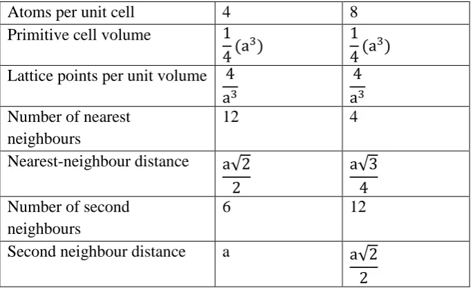
Figure 2.1: Diamond fcc lattice structure, where: 𝐚 = 𝐚𝐱 = 𝐚𝐲 = 𝐚𝐳 & 𝛃 = 𝛂 = 𝛄 = 𝟗𝟎°. The red spheres represent atoms and the silver rod are covalent bonds.
The diamond basis contains 2 atoms separated by a quarter diagonal. The tetragonal
bonds in a diamond structure are all 109.47°. (Adapted from Kittel) [26] ... 44
Figure 2.2: Diamond fcc lattice and primitive cell (in blue). The primitive cell vectors
are: A = 𝐚𝟐[𝐢 + 𝐣], B = 𝐚𝟐𝐢 + 𝐤 and C = 𝐚𝟐𝐣 + 𝐤. (Adapted from Kittel)[26]. .. 45
Table 2.1: Comparison between fcc lattice and diamond fcc lattice [26] ... 46
Figure 2.3: InSb unit cells showing the typical Zinc Blende structure in the diamond
fcc lattice. 𝐚𝐱 = 𝐚𝐲 = 𝐚𝐳 is the lattice constant. In figure 2.3(a) the indium atoms (purple) occupy one fcc ‘structure’ at [000] and the antimony atoms (blue) occupy
the other fcc structure at 𝟏𝟒𝟏𝟒𝟏𝟒. Figure 2.3(b) is of an equivalent ‘sub-lattice’
orientation of InSb where the antimony atom occupies the [000] site and the indium
atom occupies the 𝟏𝟒𝟏𝟒𝟏𝟒 sites, which is achieved by 90° rotation or translation
from (a) to (b). (Adapted from Grundmann) [29]. ... 46 Figure 2.4: Diagram demonstrating Bragg’s law in a diamond lattice. ... 49
Table 2.2: Table of the properties of silicon, germanium and Si1-xGex at 300K [31] 50
Figure 2.5: Si1-xGex alloy diamond lattice of 8 unit cells. Germanium atoms (green)
and silicon (red) occupying random sites in the lattice. ... 51
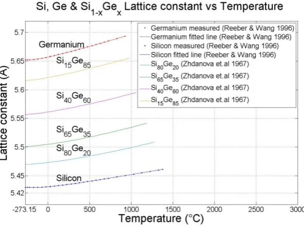
Figure 2.6: Lattice constant vs Temperature for pure silicon, pure germanium and
14
temperatures. The pure silicon and germanium plots were obtained from Reeber and Wang’s data using semi-empirical quasi-harmonic models, whilst the constant
composition Si1-xGex alloy plots were extrapolated from Zhdanova et al’s thermal
expansion data back to absolute zero. ... 53
Figure 2.7: Phase curves for binary Si1-xGex shows differences in temperatures in the
solidus and liquidus phases. ... 54
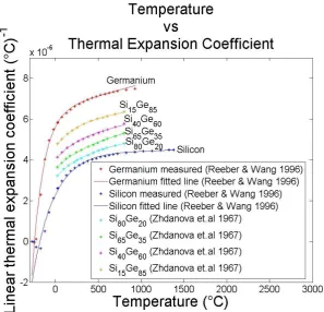
Figure 2.8: Linear thermal expansion coefficient vs Temperature plot of 𝐒𝐢𝟏 − 𝐱𝐆𝐞𝐱
alloys. For silicon and germanium, the expansion coefficient was plotted from
absolute zero up to the melting temperatures however for SiGe alloys the plots
were made using the data from Zhdanova et al in 1967 [31]. ... 55
Table 2.3: Table of the properties of binary III-V compounds with lattice constants
in-between pure silicon and pure germanium at 300K [44] [45]. ... 56
Table 2.4: Table of the properties of binary III-V compounds with lattice constants
outside of pure silicon and pure germanium at 300K [44] [45]. ... 57
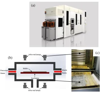
Figure 2.9: Figure (a) is an image of the ASM Epsilon 2000 RP-CVD reactor used in
this project to grow 𝐒𝐢𝟏 − 𝐱𝐆𝐞𝐱 and Ge buffer layers. Figure (b) is a cross
sectional schematic of standard CVD chamber. Figure (c) is an image taken of the
ASM Epsilon 2000 RP-CVD reactor chamber. ... 60
63
63
Figure 2.10: Diagram showing the surface reactions of dichlorosilane and germane on
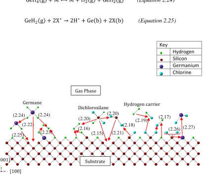
a Si(001) substrate which is initially hydrogen terminated on the surface, as a 𝐒𝐢𝟏 − 𝐱𝐆𝐞𝐱 film is deposited. Adapted from Hierlemann [54]. The numbers listed in
brackets in the diagram pertain to equations 2.15 to 2.27. ... 63
Figure 2.11: Figure (a) and (b) showing the Arrhenius function relationship between
growth rate of silicon and the reciprocal of the growth temperature when using
dichlorosilane as the precursor. Figure (a) adapted from Hierlemann et al [51] is of
silicon deposition in a rapid thermal chemical vapour deposition reactor at 2 torr
pressure and a 𝐒𝐢𝐇𝟐𝐂𝐥𝟐 𝐭𝐨 𝐇𝟐 flow rate ratio 𝐅𝐒𝐢𝐇𝟐𝐂𝐥𝟐𝐅𝐇𝟐of 0.025. Figure (b)
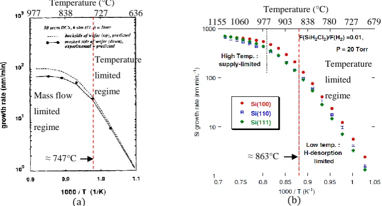
adapted from Hartmann et al [61] is of deposition in an RP-CVD reactor where 𝐅𝐒𝐢𝐇𝟐𝐂𝐥𝟐𝐅𝐇𝟐 is 0.01. ... 66
Figure 2.12: (a) Adapted from Cunningham et al [53] shows the Arrhenius function
15
temperature when using germane as the precursor. (b) Adapted from
Bogumilowicz et al [62] shows the RP-CVD growth of 𝐒𝐢𝟏 − 𝐱𝐆𝐞𝐱 layers with
various Ge contents. ... 67
Figure 2.13: Cross sectional schematic of the Gen II SS-MBE system used to grow
AlSb and InSb epilayers [66]. ... 70
Figure 2.14: Diagram showing adatom (purple) transport and growth on substrate
surface (red). (Adapted from Hudson) [69]. ... 71
Figure 2.15: (a) Czochralski silicon (001) single crystal ingot with dashed lines
showing on axis wafers to be and 6° off axis (not an accurate angle on the image)
wafers to be cut from the ingot [73]. Figure (b) shows a 100mm diameter 6° off
axis Si(001) wafer, with the marked flats indicating the (110) and (𝟏𝟏𝟎) planes.
The blue arrow indicates the direction along which surface steps lie due to cutting
the wafer at an angle from the ingot. All of the Si(001) substrates used in this
project, both on and 6° off-axis were 100mm diameter and 525µm thick. ... 73
Figure 2.16: Double domain of an on axis Si(001) substrate, created by single atomic
steps indicated by terrace A and terrace B, where the dimer orientation changes
from being parallel to the step edge (green atoms) to perpendicular to the step edge
(blue atoms). ... 73
Figure 2.17: example of III-V (pink and blue atoms) material grown on on-axis Si(001)
(red atoms). The pink atoms are the group v anions and the blue atoms are the
group III cations. The presence of the double domain means zinc blende crystals
growing on adjacent terraces would have to rotate by 90° to ensure correct bond
angles are maintained in the grown fcc lattice. ... 74
Figure 2.18: adapted from Skibitzki et al. [76] Cross sectional TEM images of 270nm
GaP grown on 𝐒𝐢𝟎. 𝟖𝟓𝐆𝐞𝟎. 𝟏𝟓/Si(001). Figure (a) is a 002 dark field HR-XTEM,
figure (b) is 𝟎𝟎𝟐 dark field and (c) 𝟎𝟎𝟐 dark field plan view image. The figures
show the presence of inversion domains generated in the GaP layer as shown by
the blue and red arrows in figure (c). ... 75
Figure 2.19: Single domain surface of an off-axis Si(001) substrate as shown by the
green silicon atoms and terrace steps (in blue). The double monolayer steps allows
the dimer bonds to maintain their orientation. This means that for zinc-blende
16
Figure 2.20: Example of III-V (pink and blue atoms) material grown on off-axis
Si(001) (red atoms). The double monolayer steps allows the dimer bonds to
maintain their orientation. This means that for zinc-blende structure grown on this
particular substrate only one sub lattice can form. Here again the group V anions
are in pink and the group III cations are in blue. ... 77
77
77
Figure 2.21: High resolution cross sectional TEM image of a Si(001) substrate offcut
toward the [110] direction at a 6° angle. ... 77 Figure 2.22: Table showing dangling bond densities for various planes of silicon,
normalised to Si(001) and the growth rate anisotropy, 𝐫𝐡𝐤𝐥, of silicon deposited at
850°C, 650°C and 600°C. Adapted from Pribat et al [84]. ... 78
Figure 2.23: Adapted from Pribat et al [84]. Figure (a) shows a Si(001) substrate with
terraces & steps and the positions of various planes. Figure (b) is a STEM image
taken by Pribat et al and shows how the thickness of a 𝐒𝐢𝟎. 𝟖𝐆𝐞𝟎. 𝟐 + Si cap +
amorphous Si film grown over a pattern etched substrate varies with respect to the
(001) surface plane. ... 79
Figure 2.24: Frank-van der Merwe growth mode of epitaxial adatoms onto a substrate.
... 80
Figure 2.25: Volmer-Weber growth mode of epitaxial adatoms onto a substrate. .... 81
Figure 2.26: Stranski-Krastanov growth mode of epitaxial adatoms onto a substrate.
... 81
Figure 2.27: Diagrams showing epitaxial layer atoms (in purple) under compressive
strain (a) and under tensile strain (b), with respect to the substrate (in red). ... 83 Figure 2.28: (a) Burgers circuit around an edge dislocation: [MNOPQ] and (b)
equivalent burgers circuit in a dislocation free crystal [MNOP]. The outstanding
vector required to close the circuit in figure (b), [MQ], is known as the burgers
vector. Taken from Hull and Bacon[30]. ... 86
Figure 2.29: (a) Burgers circuit around a left-hand screw dislocation with a positive
line sense: [MNOPQ] and (b) equivalent burgers circuit in a dislocation free crystal
[MNOP] with the burgers vector shown as [MQ]. Taken from Hull and Bacon [30].
... 86
Figure 2.30: Vector diagram showing: Burgers vector and line direction for a 60° misfit
17
The (𝟏𝟏𝟏) glide plane is the same as the (𝟏𝟏𝟏) glide plane except the normal
vector is pointing down instead of up. ... 87
2.5.5. Threading dislocations ... 89
Figure 2.31: Diagram showing a [110] misfit dislocation along glide plane in an FCC diamond or zinc blende crystal, “threading” through the broken bonds. Taken from
Shah [96]. ... 89
Figure 2.32: Diagram showing the glide of a [110] 60° misfit dislocation extending
and gliding along the (111) glide plane in an FCC diamond or zinc blende crystal.
Adapted from Shah [96]. ... 90
Figure 2.33: Diagram showing the progression of the Frank-Read dislocation
multiplication process. Taken from Hull and Bacon [30]. ... 92
Figure 2.34: Diagram showing the Matthews-Blakeslee model for misfit dislocation
propagation in a situation where the epilayer is compressively strained to the
substrate. Adapted from Halpin [101]. ... 93
Figure 2.35: Diagram showing the nucleation of a half loop on a strained epilayer
surface, expanding radially until a misfit dislocation is formed at the interface. . 95
Figure 2.36: Interaction of a gliding threading dislocation with a strain field created by
an orthogonal misfit dislocation. The threading dislocation has been forced into a
reduced glide channel h* by the retarding force of the strain field 𝑭𝒅. Adapted
from Freund [111]. ... 97
Figure 2.37: Vector diagram showing a 60° misfit dislocation in a FCC diamond (zinc
blende) crystal, and the Shockley partial dislocations at 90° with a Burgers vector
of 𝐛𝟗𝟎 = 𝐚𝟔[𝟏𝟏𝟐] and 30° with a Burgers vector of 𝐛𝟑𝟎 = 𝒂𝟔[𝟏𝟐𝟏]. ... 98
Figure 2.38: Force balance diagram of a disassociated 60° misfit dislocation and its
two Shockley partial dislocations under strain on a (001) substrate. ... 99
Table 2.5: 𝐅𝐬𝐭𝐫𝐚𝐢𝐧 for the two Shockley partial dislocations. ... 99
Figure 2.39: Creation of tilt in pseudomorphic epitaxial layer (red) due to the Poisson
effect on a vicinal (offcut) substrate (black). The blue dashed line is the growth
surface. Adapted from Nagai [114]. ... 101 Figure 2.40: Diagram showing of how a ‘V’ shaped crack penetrates to a depth, d,
through the epitaxial layer of thickness, h, during strain relaxation on the substrate.
18
Figure 3.1: JEOL 2100 TEM (a) and cutaway schematic diagram of TEM (b). The
arrows in figure (a) point to the location of the various parts inside the instrument.
Figure (b) shows the instrument in normal imaging mode, as indicated by the
electron beam (in red). ... 105
Figure 3.2: Cleave lines on an (001) orientation 100mm diameter epiwafer. For off
axis substrates, where the offcut steps lie towards the [110] direction the cleaving
process requires cleaving parallel to a step first i.e. perpendicular to the (𝟏𝟏𝟎)
plane, to ensure more evenly shaped wafer pieces. ... 108
Figure 3.3: cross sectional TEM sample preparation process. ... 109
Figure 3.4: Plan view sectional TEM sample preparation process. ... 109
Figure 3.5: Diffraction mode on the TEM. Figure (a) shows the TEM in diffraction
mode. This is achieved by adjusting the magnetic field strength of the projector
lens which in turn allows the image from the back focal plane to be displayed on
the florescent screen. Figure (b) is an image taken of the TEM phosphorous screen
in diffraction mode whilst setting up a two beam condition showing the Kikuchi
lines on the [001] zone axis, and the straight though beam on the 𝟐𝟐𝟎 Kikuchi line
and the Bragg peak on the 220 Kikuchi line. ... 111
Figure 3.6: Stereographic [001] Kikuchi line map for FCC diamond and zinc blende
crystals [122]. The [001] zone axes is indicated by the red dashed circle. ... 112
Figure 3.7: (a) represents the condition when 𝐠 ∙ 𝐛 = 𝟎, i.e. the diffraction vector and
Burgers vector are orthogonal to each other and only residual contrast is seen.
Figure (b) shows the condition where 𝐠 and 𝐛 are parallel, therefore the distortion
caused by the dislocation is visible. Taken from Shah [96]. ... 113 Figure 3.9: Image of the Panalytical X’pert Pro X-ray diffractometer used in this study.
... 115
116
Figure 3.10: ω-2θ coupled scan set up. The sample (in red) is taped to the stage. The
angle χ has been referred to as ψ in some references however, the term χ has been
adopted as it is the standard Synchrotron notation. ... 116
Figure 3.11: Diagram of the Ewald sphere intersecting the 004 Bragg peak showing the satisfaction of Bragg’s law for the (004) plane. 𝐤 is the incident wavevector
and 𝐤′ is the diffracted wavevector. The origin of reciprocal space is shown as
19
𝛌𝟐𝐝𝐡𝐤𝐥. The distances of the 004 and 224 Bragg peaks are shown with respect to
the origin as reciprocal lattice units. ... 117
Figure 3.12: (004) crystal planes (a) and (224) (intercepts at 𝟏𝟒, 𝟏𝟒, 𝟏𝟐) planes (b) for
FCC diamond crystals. The arrows shown are the surface normal vectors. The
green plane in figure (a) shows the (002) plane that obeys the structure factor
equation for zinc blende crystals and therefore is allowable. ... 119
Table 3.1: Bragg angles for Si, Ge, AlSb and InSb for the 004 and 224 reflections
including the tilt corrected angles for the 224 reflections. The tilt corrected angle
for InSb224 is very small however it is still obtained and so a different assymetric
reflection was not chosen for the InSb layer. ... 120
Figure 3.13: Reciprocal space map for FCC diamond and zinc blende crystals
orientated in the (001) plane as the incident beam, ω, is rotated about the sample at
half the rate of the detector rotation so as to maintain a constant ratio of 𝝎𝟐𝜽. The
blue regions are known as forbidden reflections and only the Bragg peaks in the
white regions are accessible. Adapted from Bowen [125]. ... 121
Figure 3.14: Analysis of 004 and 224 RSMs. The InSb layer is included to show peak
positioning based on lattice constant of the crystal. The larger the lattice constant
in bulk form, the closer the peak sits towards the origin [000]. ... 122
Figure 3.15: Figure (a) shows the step and terrace surface of an off-axis substrate.
Figure (b) shows the importance of sample orientation of the off-axis grown sample
with (110) plane perpendicular to the incident beam in order to initially align to the
substrate. If the sample was mounted with the (110) plane horizontally and the (𝟏𝟏𝟎) vertically then a wide χ scan wide be required to pick up the substrate peak.
... 124
Figure 3.16: (a) Veeco Multimode AFM, (b) SiN AFM cantilever and tip [127] and (c)
AFM head with labelled parts [128]. ... 125
Figure 3.17: Lennard-Jones force between sample and tip, Fts (red), plotted with
cantilever spring constant forces (in blue) the gradient of which is k. Taken from
Voigtlander [129]. ... 126
Figure 3.18: Diagram of a DIC (Normaski) optical microscope. Adapted from Nash
[131]. ... 130
Figure 3.19: (a) Ge composition in 𝐒𝐢𝟏 − 𝐱𝐆𝐞𝐱 vs Schimmel etch rate investigation
20
graded 𝐒𝐢𝟏 − 𝐱𝐆𝐞𝐱/𝐆𝐞 buffer layers vs Schimmel and Iodine etch rate carried out
by Shah in 2009 [96]. ... 134
Figure 4.1: (a) LT Ge/Si(001) buffer structure. The Ge buffer layers in this low temperature study were grown between T = 300°C and 400°C. The thicknesses ranged from (t) = 2nm to 351nm. (b) In the annealing study, the Ge buffer layers were grown between 20nm and 78nm thickness and then annealed for either 1min or 5mins. ... 140
Table 4.1: 400°C Ge growth temperature buffer samples ... 141
Table 4.2: 350°C Ge buffer growth temperature buffer samples ... 142
Table 4.3: 300°C Ge buffer growth temperature buffer samples ... 142
Figure 4.2: X-TEM of samples grown at 400°C. Samples: 15-42 (a), 15-41 (b), 14-295 (c), 14-297 (d), 14-299 (e) and 15-38 (f). Diffraction contrast TEM allows the thickness to be ascertained using the 004 diffraction condition. ... 144
Figure 4.3: X-TEM of samples grown at 350°C. Samples: 15-46 (a), 15-45 (b), 14-300 (c), 14-302 (d), 15-53 (e) and 15-43 (f): Ge buffer layer grown at 350°C with increasing thickness from (a) to (f). The thickness measurements were ascertained from the 004 diffraction condition. Notice that the layer is relatively smooth and planar until approximately at 95nm thickness, after which faceting takes place. ... 145
Figure 4.4: X-TEM of samples grown at 300°C. Samples: 15-50 (a), 15-49 (b), 15-48 (c) and 14-304 (d). ... 146
Figure 4.5: Comparison of Ge buffer layers grown at 300°C, 350°C and 400°C to roughly similar thicknesses. Figure (a) X-TEM of sample 15-47; Ge grown at 300°C to 78.9nm thickness. Figure (b) X-TEM of sample 14-301; Ge buffer layer grown at 350°C and figure (c) X-TEM of sample 14-296; Ge buffer layer grown at 400°C. ... 147
Figure 4.6: Growth time vs thickness plots for Ge grown at various temperatures. Due to insufficient samples and higher error in thickness measurements for samples grown at 300°C the stagnation time and growth rate could not accurately calculated but given the location of the points, it would seem that the stagnation time is longer and the growth rate lower for 300°C grown Ge buffer layers. ... 148
Table 4.4: Annealing study on LT thin Ge buffer layers. ... 149
Figure 4.7: (a) 220 dark field X-TEM image of sample 15-56; 20nm Ge buffer layer
X-21
TEM image of sample 15-57; 20nm Ge buffer layer grown at 300°C and then
annealed at 650°C for 5 minutes. ... 149
Figure 4.8: (a) 220 dark field X-TEM image of sample 15-58; 20nm Ge buffer layer
grown at 400°C and then annealed at 650°C for 1 minute and (b) 220 dark field
X-TEM image of sample 15-59; 20nm Ge buffer layer grown at 400°C and then
annealed at 650°C for 5 minutes. Thickness were measured from the 004
diffraction condition. ... 151
Figure 4.9: (a) 220 dark field X-TEM image of sample 15-60; 78nm Ge buffer layer
grown at 400°C and then annealed at 650°C for 1 minute and (b) 220 dark field X-TEM image of sample 15-61; 78nm Ge buffer layer grown at 400°C and then
annealed at 650°C for 5 minutes. Thicknesses were measured from the 004
diffraction condition. ... 152
Figure 4.11: 3D 20µm x 20µm AFM micrographs of Ge buffer layers grown at 350°C,
plotted in increasing thickness. The sample numbers are labelled to the right of
each micrograph. The rms roughness (Rrms) and maximum to minimum heights
(h) are listed as well. ... 154
Figure 4.12: 3D 20µm x 20µm AFM micrographs of Ge buffer layers grown at 300°C
as shown in table 4.3. The sample numbers are labelled to the right of each
micrograph and are listed in order of thickness on the z-axis. The rms roughness
(Rrms) and maximum to minimum heights (h) are listed as well. ... 156
157
Figure 4.13: Contact mode AFM micrographs of Ge buffer layers grown to 20nm
thickness and annealed at 650° as per table 4.4. Figure (a) is of Ge layers grown at
300°C, (b) is of Ge layers grown at 400°C... 157
Figure 4.14: Contact mode AFM micrographs of Ge buffer layers grown to 78nm
thickness and annealed at 650° for 1min and 5 mins. Annealing a 400°C 78nm
layer for 4 more mins doesn’t affect the roughness. ... 158
Figure 4.15: Roughness (rms) vs thickness plot for the Ge buffer layers grown at
various temperatures. ... 159
Figure 4.16: AFM scan height difference vs thickness plot for the Ge buffer layers
grown at various temperatures... 160
Figure 4.18: HR-XRD 004 (a) and 224 (b) RSM of sample 15-47: Ge buffer layer
22
Figure 4.19: HR-XRD 004 (a) and 224 (b) RSM of sample 15-43: Ge buffer layer
grown to 174nm thickness at 350°C. ... 163
Figure 4.20: HR-XRD 004 (a) and 224 (b) RSM of sample 15-38: Ge buffer layer
grown to 351nm thickness at 400°C. ... 164
Figure 4.21: HR-XRD 004 (a) and 224 (b) RSM of sample 15-61 grown at 400°C and
annealed at 650°C for 5mins. ... 164
Figure 4.22: Strain in the LT Ge buffer layer measured using HR-XRD, grown at
various temperatures and plotted against thickness. The error in the TEM thickness
measurements is +/-0.5%. ... 165 Figure 4.24: HR-XTEM of sample 15-46. Stacking faults propagating from a single
stair-rod dislocation, can be seen. The measured angle from either stacked section
of the layer is 55° along [110] direction. ... 166
Figure 4.25: Plan view TEM of sample 15-47 (300°C growth 78.9nm thickness)
showing threading dislocations. TDD for this image is 𝟏. 𝟎𝟓 × 𝟏𝟎𝟏𝟏 𝐜𝐦 − 𝟐.
Average TDD for this sample is 𝟗. 𝟖𝟔 × 𝟏𝟎𝟏𝟎 𝐜𝐦 − 𝟐. ... 167
Figure 4.26: Plan view TEM of sample 14-300 (350°C growth, 42nm thickness)
showing 2D defects as indicated by the red dashed circles, possibly emanating from
the stair rod dislocations. The angle measured between 2D defects is 125°. ... 167
Figure 4.27: Plan view TEM of sample 15-43 (350°C growth 174nm thickness). TDD
for this image is 𝟐. 𝟑𝟐 × 𝟏𝟎𝟏𝟎 𝐜𝐦 − 𝟐. Average TDD for this sample is 𝟐. 𝟑𝟎 × 𝟏𝟎𝟏𝟎 𝐜𝐦 − 𝟐 ... 168
Figure 4.28: Plan view TEM of sample 14-302 (350°C growth and 95nm thickness)
showing Moiré fringes on the left and side of the image caused by the interference
between the substrate diffraction vector and the thin partially relaxed epilayer
diffraction vector. Average TDD for this sample is 𝟔. 𝟏𝟓 × 𝟏𝟎𝟏𝟎 𝐜𝐦 − 𝟐. .... 168
Figure 4.29: Plan view TEM of sample 15-38 (400°C growth, 351nm thickness). TDD
for this image is 𝟗. 𝟏𝟑 × 𝟏𝟎𝟗 𝐜𝐦 − 𝟐. Average TDD for this sample is 𝟖. 𝟔𝟏 × 𝟏𝟎𝟗 𝐜𝐦 − 𝟐. ... 169
Figure 4.30: Plan view TEM of sample 15-61 (400°C growth + 650°C for 5 mins 78nm
thickness). TDD for this image is 𝟔. 𝟏𝟖 × 𝟏𝟎𝟗 𝐜𝐦 − 𝟐. Average TDD for this
sample is 𝟕. 𝟓𝟕 × 𝟏𝟎𝟗 𝐜𝐦 − 𝟐. ... 170
Figure 4.31: Threading dislocation density vs thickness for LT-Ge buffer layers .. 171
23
Figure 5.1: Schematic of the linearly graded buffer structure. The graded layer was
created by adjusting F(GeH4) whilst keeping the flowrate of DCS constant. The
growth temperature was kept fixed at 850°C. ... 179
Figure 5.2: Linearly graded Si1-xGex buffer layer samples grown on on-axis Si(001).
Listed in order of increasing grading rate... 181
Figure 5.3: X-TEM image of sample 13-101 linearly graded to Si0.854Ge0.146 buffer
layer total thickness is 2020nm 10nm with a grading rate of 13.64%Ge/µm
+/-5%. Rrms = 1.27nm. The green dashed circles indicate Frank-Read loops. ... 181
Figure 5.4: 004 and 224 HR-XRD RSM of sample 13-101, linearly graded to
Si0.854Ge0.146. Total buffer layer thickness is 2020nm +/-10nm with a grading rate
of 13.4%Ge/µm +/-5%. ... 182
Figure 5.5: (a) 20µm x 20µm Contact mode AFM of 13-101, linearly graded to
Si0.854Ge0.146. Rrms = 1.27nm 0.2nm. Total buffer layer thickness is 2020nm
+/-10nm with a grading rate of 13.4%Ge/µm +/-5%. Figure (b) is a plan view TEM
image of an etch pit showing a threading dislocation at the centre of the pit. ... 183
Figure 5.6: DIC optical microscope images of sample 13-101 Si0.854Ge0.146 after
Schimmel etching for different periods of time (a) - (f), revealing threading
dislocations. Total buffer layer thickness is 2020nm +/-10nm with a grading rate
of 13.4%Ge/µm +/-1%. Average TDD (pile up + field) taken from images etched
for 430 secs = 𝟗. 𝟏𝟎 × 𝟏𝟎𝟕𝐜𝐦 − 𝟐. The two red orthogonal ellipses in the diagram
indicate pile up of threading dislocations and the blue circles shows field threading
dislocations. ... 184
Figure 5.7: X-TEM image of sample 13-119 linearly graded to Si0.665Ge0.335 buffer
layer total thickness is 1093nm +/-5.5nm with a grading rate of 56%Ge/µm +/-1%.
Rrms = 4.73nm. ... 185
Figure 5.8: 50µm x 50µm contact mode AFM of sample 13-119 linearly graded to
Si0.665Ge0.335 buffer layer total thickness is 1093nm +/-10nm with a grading rate of
56%Ge/µm +/-1%. Rrms = 4.73nm. Strong cross hatching is seen as well as large
pits along cross hatch lines indicating merging of pile-up TDs into large pits. . 185
Figure 5.9: HR-XRD of sample 13-119, linearly graded to Si0.665Ge0.335. Buffer layer
total thickness is 1093nm +/-10nm with a grading rate of 56%Ge/µm +/-1%. Notice
the large tilt in SiGe epilayer possibly due to strain relaxation vis the modified
24
Figure 5.10: DIC optical microscope image of sample 13-119 linearly graded to
Si0.665Ge0.335 buffer layer total thickness is 1093nm +/-10nm with a grading rate of
56%Ge/µm +/-1%. The sample has been Schimmel etched for 190 secs. Average
TDD (pile up + field) = 𝟓. 𝟐𝟔 × 𝟏𝟎𝟕𝐜𝐦 − 𝟐. The two red orthogonal ellipses in
the diagram indicate pile up of threading dislocations. ... 186
Figure 5.11: X-TEM image of sample 13-121 linearly graded to Si0.364Ge0.636 buffer
layer total thickness is 1092nm 10nm with a grading rate of 135.9%Ge/µm
+/-1%. Rrms = 26.43nm. The green dashed circle is of a dislocation loop that has
penetrated into the substrate. ... 187
Figure 5.12: HR-XRD of sample 13-121, linearly graded to Si0.364Ge0.636 Total buffer
layer thickness is 1092nm +/-10nm with a grading rate of 135.9%Ge/µm +/-1%.
... 188
Figure 5.13: Plan view TEM of sample 13-121: linearly graded to Si0.364Ge0.636 Total
buffer layer thickness is 1092nm 10nm with a grading rate of 135.9%Ge/µm
+/-1%. Average TDD (pile up + field) = 𝟏. 𝟓𝟖 × 𝟏𝟎𝟗𝐜𝐦 − 𝟐. The red circles
highlight 2D defects (possibly micro twins) and the arrows point to threading
dislocations. ... 188
Figure 5.14: Schematic of the reverse linearly graded buffer structure. The LT Ge was
grown at 350°C and the HT Ge was grown at 550°C using 𝐆𝐞𝐇𝟒. The graded layer
was created by adjusting 𝐅(𝐒𝐢𝐂𝐥𝟐𝐇𝟐) whilst keeping the flowrate of 𝐆𝐞𝐇𝟒
constant. The growth temperature of the 𝐒𝐢𝟏 − 𝐱𝐆𝐞𝐱was kept fixed at 850°C. 189
Figure 5.15: List of reverse linearly graded 𝐒𝐢𝟏 − 𝐱𝐆𝐞𝐱 buffer layer samples. The
samples are listed in order of increasing grading rate, except the bottom two rows,
in pink, which were grown on off-axis Si(001) ... 190
Figure 5.16: (a) X-TEM of 310nm LT/HT Ge buffer layer. (b) 220 plan view TEM
image, Average TDD = 𝟏. 𝟎𝟏 × 𝟏𝟎𝟗𝐜𝐦 − 𝟐 ± 𝟏𝟎%. 𝐑𝐫𝐦𝐬 = 𝟐. 𝟐𝟓𝐧𝐦. Typical
length of threading dislocation is 151nm. ... 191
Figure 5.17: X-TEM of 445nm LT/HT Ge buffer layer Average TDD = 𝟑 × 𝟏𝟎𝟖𝐜𝐦 − 𝟐 ± 𝟏𝟎%. 𝐑𝐫𝐦𝐬 = 𝟏. 𝟒𝟔𝐧𝐦. ... 191
Figure 5.18: X-TEM of 765nm LT/HT Ge buffer layer Average TDD = 𝟏 × 𝟏𝟎𝟖𝐜𝐦 − 𝟐 ± 𝟏𝟎%. 𝐑𝐫𝐦𝐬 = 𝟎. 𝟕𝟔𝐧𝐦. ... 192
Figure 5.19: X-TEM of sample 13-134, reverse linearly graded to Si0.55Ge0.45. Buffer
25
+/-10%. The surface appears to be free of severe undulation formation due to
tensile strain relaxation. ... 193
Figure 5.20: X-TEM of sample 13-134, reverse linearly graded to Si0.55Ge0.45. Buffer
layer total thickness is 7584nm 10nm with a grading rate of 21.4%Ge/µm
+/-1%. ... 194
Figure 5.21: X-TEM of sample 13-134, reverse linearly graded to 𝑺𝒊𝟎. 𝟓𝟓𝑮𝒆𝟎. 𝟒𝟓/𝑮𝒆
magnified at the top of the constant composition region. A partially visible stacking
fault is seen by the position of its partial dislocations. ... 195
Figure 5.22: X-TEM of sample 13-134, reverse linearly graded to Si0.55Ge0.45. at the
interface between the Si(001) substrate and the Ge underlayer showing Lomar
dislocations. ... 195
Figure 5.23: 20µm x 20µm contact mode AFM micrograph of sample 13-165, reverse
linearly graded to 𝐒𝐢𝟎. 𝟐𝟖𝟑𝐆𝐞𝟎. 𝟕𝟏𝟕/𝐆𝐞. Threading dislocations can be seen from
the scan. The estimated TDD from the AFM scan ≈ 𝟐 × 𝟏𝟎𝟕𝐜𝐦 − 𝟐 which is
lower than the value measured through Schimmel etching of the sample.
Rrms=2.42nm ... 196
Figure 5.24: 20µm x 20µm contact mode AFM micrograph of sample 13-134, reverse
linearly graded to 𝐒𝐢𝟎. 𝟓𝟓𝐆𝐞𝟎. 𝟒𝟓/𝐆𝐞. Stacking faults can be seen on the surface,
indicated by the dashed white line in figure (b). Rrms=3.7nm. ... 196
Figure 5.25: HR-XRD of sample 13-165, reverse linearly graded to Si0.283Ge0.717.
Negligible tilt with respect to Si(001) is observed in the epilayers. 0.006°, 0.002°
and 0.005° tilt was measured in the Ge underlayer, Si0.051Ge0.949 epilayer and
Si0.283Ge0.717 epilayer respectively. ... 198
Figure 5.26: HR-XRD of sample 13-134, reverse linearly graded to Si0.55Ge0.45. 0° tilt
in the Ge underlayer, Si0.043Ge0.957 and Si0.55Ge0.45 epilayers. Severe peak
broadening in the Si0.55Ge0.45 layer is due to the rise in stacking faults. ... 198
Figure 5.27: HR-XRD of sample 13-162, reverse linearly graded to Si0.292Ge0.708 on 6°
off-axis Si(001). The measured tilt in the epilayers were as following: 0.231° in the
Ge underlayer, 0.221° in the Si0.0.52Ge0.948 epilayer and 0.221° Si0.292Ge0.708
epilayer. Strain in the Ge underlayer was 0.24% and strain in the Si0.292Ge0.708
epilayer was 0.22%. ... 199
Figure 5.28: 2 min Schimmel etch and DIC optical microscopy of sample 13-165,
26
𝟓. 𝟐𝟗 (±𝟎. 𝟓𝟐𝟗) × 𝟏𝟎𝟕𝐜𝐦 − 𝟐. This image is an example of a reverse linearly
graded buffer. As can be seen, pile-up of threading dislocations does not occur.
... 200
Figure 5.29: 2 min Schimmel etch and DIC optical microscope image of sample
13-134, reverse linearly graded Si0.55Ge0.45/Ge buffer. Average TDD ≈
𝟑. 𝟓𝟑 (±𝟎. 𝟑𝟓𝟑) × 𝟏𝟎𝟕𝐜𝐦 − 𝟐. The black dots are threading dislocations whilst
the straight lines are stacking faults highlighted by the red ellipses. ... 201
Figure 5.41: X-TEM of sample 13-165, reverse linearly graded to Si0.283Ge0.717. Buffer
layer total thickness, h, is 5535nm +/-15nm with a grading rate of 12.72%Ge/µm
+/-10%. The relaxation of the Ge underlayer is 104.95% with respect to the
substrate and the 𝐒𝐢𝟎. 𝟐𝟖𝟑𝐆𝐞𝟎. 𝟕𝟏𝟕 layer with respect to the substrate is 106.48%.
The crack penetration depth, d, is measured to be 6.02µm. The crack width, w, is
measured to be 0.0617µm. ... 212
Figure 5.42: 2 min Schimmel etch and DIC optical microscope image of sample
13-165, reverse linearly graded to Si0.283Ge0.717/Ge showing cracks. The crack line
density for this sample, 𝛒𝐂𝐃 = 𝟗𝟎. 𝟖𝟑 𝐜𝐦 − 𝟏. The distance between cracks
varies and at the lowest possible magnification (x20) the number of cracks in two
directions, perpendicular to each other, was counted over a measured distance.
... 212
Figure 5.43: Plot of Ge composition (%) vs cleaved crack density for 𝐒𝐢𝟏 − 𝐱𝐆𝐞𝐱/𝐆𝐞
buffer layers. A trend is seen where the cleaved crack density reduces with
reducing Ge content. ... 213
Figure 5.45: Schematic no. 1 of the reverse step graded buffer structure graded to 𝐒𝐢𝟎. 𝟏𝐆𝐞𝟎. 𝟗. The LT Ge was grown at 350°C and the HT Ge was grown at 550°C
using 𝐆𝐞𝐇𝟒. The step graded layer was created by adjusting 𝐅(𝐒𝐢𝐂𝐥𝟐𝐇𝟐) whilst
keeping the flowrate of 𝐆𝐞𝐇𝟒 constant so as to solve equation 2.45 for x=0.9. 214
Figure 5.46: Schematic no. 2 of the reverse step graded buffer structure. The buffer
growth conditions are identical as with schematic no. 1, however the 𝐒𝐢𝟏 − 𝐱𝐆𝐞𝐱
layer is grown for 3 minutes therefore based on figure 5.39, it is assumed that the
step layers with lower Ge content will have a faster growth rate and therefore
thicker layers. In the 𝐒𝐢𝟏 − 𝐱𝐆𝐞𝐱 layer, x is calculated to be between 0.95 and 0.55
27
Figure 5.47: List of samples of reverse step graded 𝐒𝐢𝟏 − 𝐱𝐆𝐞𝐱/𝐆𝐞 buffer layers. As
will be seen in the results section, reverse step grading to lower Ge content layers
has the effect of creating two separate layers. ... 215
Figure 5.48: X-TEM of sample 15-72: 930nm LT/HT Ge buffer layer Average TDD
= 𝟔. 𝟏𝟗 × 𝟏𝟎𝟕𝐜𝐦 − 𝟐 ± 𝟏𝟎%. 𝐑𝐫𝐦𝐬 = 𝟎. 𝟗𝟐𝐧𝐦. The cross-sectional image
shows the Ge buffer layer to be of very high crystalline quality. ... 216
Figure 5.49: TEM of sample 15-72 at the interface between the Ge epilayer and Si(001)
substrate. Stacking faults can be seen at the interface; presumably from the 350°C
layer and Lomer dislocations. The interface between the 550°C and 350°C layers
cannot be distinguished. ... 216
Figure 5.50: HR-XTEM of sample 15-72 at lattice resolution. The distance measured
in the image between Lomer dislocations is approximately 11nm +/- 0.05nm. 217
Figure 5.51: 004 and 224 HR-XRD RSM of sample 15-72: 930nm LT/HT Ge buffer
layer. The strain in the layer is 0.22% tensile strain. The sharp Ge peak indicates
low defect density in the layer. ... 218
Figure 5.52: Plan view TEM of sample 15-72 930nm LT/HT Ge underlayer. A typical
threading dislocation length is shown. ... 218
Figure 5.53: X-TEM of sample 15-73 RSG 𝐒𝐢𝟎. 𝟏𝐆𝐞𝟎. 𝟗/𝐆𝐞 buffer layer. The total
thickness of the structure = 1108nm +/-5nm. The thickness of the 𝐒𝐢𝟎. 𝟏𝐆𝐞𝟎. 𝟗
buffer layer is estimated from 004 diffraction image as 228nm +/- 20nm. ... 219
Figure 5.54: Contact mode AFM of (a) sample 15-72 930nm LT/HT Ge underlayer:
Rrms= 0.92nm, height =15.1nm (b) sample 15-73 RSG 𝐒𝐢𝟎. 𝟏𝐆𝐞𝟎. 𝟗/𝐆𝐞 buffer
layer: Rrms= 2.53nm, height =21.2nm... 220
Figure 5.55: Plan view TEM of sample 15-73 RSG 𝐒𝐢𝟎. 𝟏𝐆𝐞𝟎. 𝟗/𝐆𝐞 buffer layer. The
average TDD of the sample is 𝟐. 𝟓𝟕 × 𝟏𝟎𝟗𝐜𝐦 − 𝟐. This is a factor of x100 more
threading dislocations than in the Ge underlayer. ... 220
Figure 5.56: 004 and 224 HR-XRD RSM of sample 15-73: 1108nm RSG 𝐒𝐢𝟎. 𝟏𝐆𝐞𝟎. 𝟗/𝐆𝐞 buffer layer. The broadening of the 𝐒𝐢𝟎. 𝟏𝐆𝐞𝟎. 𝟗 peak is due to
a greater density of defects in the layer compared to the Ge underlayer. ... 221
Figure 5.57: X-TEM of sample 15-77 RSG 𝐒𝐢𝟎. 𝟏𝟔𝐆𝐞𝟎. 𝟖𝟒/𝐆𝐞 buffer layer. When
depositing a 𝐒𝐢𝟎. 𝟏𝟔𝐆𝐞𝟎. 𝟖𝟒 layer; the interface at the Ge underlayer has been
disturbed. HR-XRD shows that two compositions of 𝐒𝐢𝟏 − 𝐱𝐆𝐞𝐱 are present. One
28
to determine where each of the layers are from the TEM image. The maximum
measured thickness of the entire heterostructure in the 004 diffraction condition is
1388nm. ... 221
Figure 5.58: 004 and 224 HR-XRD RSM of sample 15-77: RSG 𝐒𝐢𝟎. 𝟏𝟔𝐆𝐞𝟎. 𝟖𝟒/𝐆𝐞
buffer layer. A 𝐒𝐢𝟎. 𝟏𝟕𝐆𝐞𝟎. 𝟖𝟑 layer is also seen from the RSMs. The 224 RSM
shows that the 𝐒𝐢𝟎. 𝟏𝟕𝐆𝐞𝟎. 𝟖𝟑 layer is strained with respect to the 𝐒𝐢𝟎. 𝟏𝟔𝐆𝐞𝟎. 𝟖𝟒
layer and is 0.018° tilted with respect to the substrate. ... 222
Figure 5.59: Contact mode AFM of sample 15-77. The Rrms = 71.5nm and height is
709nm. The starting roughness in the Ge underlayer is 0.92nm. This is the
maximum roughness recorded for the RSG buffer layers. This suggests that strain
relief through the formation of surface undulations is at its maximum here. .... 222
Figure 5.60: Plan view TEM of sample 15-77: RSG 𝐒𝐢𝟎. 𝟏𝟔𝐆𝐞𝟎. 𝟖𝟒/𝐆𝐞 buffer layer.
Average 𝐓𝐃𝐃 = 𝟓. 𝟑𝟓 (±𝟎. 𝟓𝟒) × 𝟏𝟎𝟖𝐜𝐦 − 𝟐. ... 223
Figure 5.61: X-TEM of sample 15-74 RSG 𝐒𝐢𝟎. 𝟐𝟖𝐆𝐞𝟎. 𝟕𝟐/𝐆𝐞 buffer layer. Total
thickness = 1560nm. Reverse step grading to 𝐒𝐢𝟎. 𝟐𝟖𝐆𝐞𝟎. 𝟕𝟐 has caused the layer
to separate into two distinct compositions, as verified through HR-XRD, of 𝐒𝐢𝟎. 𝟑𝟎𝐆𝐞𝟎. 𝟕𝟎 and 𝐒𝐢𝟎. 𝟐𝟏𝐆𝐞𝟎. 𝟕𝟗. The positions of these two layers is
estimated on the TEM image based on the locations of misfit dislocations. ... 223
Figure 5.62: HR-XRD of sample 15-74: RSG 𝐒𝐢𝟎. 𝟐𝟖𝐆𝐞𝟎. 𝟕𝟐/𝐆𝐞 buffer layer. Total
thickness = 1560nm. Reverse step grading to 𝐒𝐢𝟎. 𝟐𝟖𝐆𝐞𝟎. 𝟕𝟐 has caused the layer
to separate into two separate compositions of 𝐒𝐢𝟎. 𝟑𝟎𝐆𝐞𝟎. 𝟕𝟎 and 𝐒𝐢𝟎. 𝟐𝟏𝐆𝐞𝟎. 𝟕𝟗.
It is assumed that the 𝐒𝐢𝟎. 𝟑𝟎𝐆𝐞𝟎. 𝟕𝟎 is on top and the 𝐒𝐢𝟎. 𝟐𝟏𝐆𝐞𝟎. 𝟕𝟗 is on the
bottom. All of the epilayers are under some degree of tensile strain, with the 𝐒𝐢𝟎. 𝟑𝟎𝐆𝐞𝟎. 𝟕𝟎 layer being under a slightly higher tensile strain of 0.43% and the
𝐒𝐢𝟎. 𝟐𝟏𝐆𝐞𝟎. 𝟕𝟗 being more relaxed at 0.16% tensile strain. ... 224
Figure 5.63: Focused ion beam-SEM image of sample 15-74 showing the presence of
voids in the epilayer. The argon ion beam was used to dig a trench in the sample
and then the sample was tilted to see a cross section. This was done to see a larger
cross-section of the epilayer, since X-TEM only gives a limited region of thin area.
As can be seen from the image, spherical voids are present in the epilayer. ... 225
Figure 5.64: SEM image of sample 15-74, confirming the presence of voids in the
29
epilayer from the SEM image. The average distance between voids is about 1.3µm.
... 226
Figure 5.65: Contact mode AFM of sample 15-74: RSG 𝐒𝐢𝟎. 𝟐𝟖𝐆𝐞𝟎. 𝟕𝟐/𝐆𝐞. Rrms=
52.6nm, height = 418nm. The real composition of the layer is: 𝐒𝐢𝟎. 𝟑𝟎𝐆𝐞𝟎. 𝟕𝟎/ 𝐒𝐢𝟎. 𝟐𝟏𝐆𝐞𝟎. 𝟕𝟗/𝐆𝐞. ... 226
Figure 5.66: Plan view TEM of sample 15-74. Sample average 𝐓𝐃𝐃 = 𝟓. 𝟎𝟒 (±𝟎. 𝟓) × 𝟏𝟎𝟖𝐜𝐦 − 𝟐. ... 227
Figure 5.67: (004) diffraction condition bright field X-TEM of sample 15-75. The
voids are clearly seen in the Ge underlayer. The average total thickness of the
buffer layer is approximately 1638 nm. The average spacing between voids is
2.2µm. ... 227
Figure 5.68: X-TEM of sample 15-75: RSG 𝐒𝐢𝟎. 𝟒𝟓𝐆𝐞𝟎. 𝟓𝟓/𝐆𝐞. The total thickness
of the layer is 1638nm (measured in the 004 diffraction condition). Silicon atoms
from the SiGe epilayer can be seen diffusing through the Ge underlayer and meeting the Lomer interface between the Ge underlayer and the Si substrate. The
estimated thickness of the 𝐒𝐢𝟎. 𝟐𝟏𝐆𝐞𝟎. 𝟕𝟗 layer is 322nm +/- 15nm and the 𝐒𝐢𝟎. 𝟓𝟑𝐆𝐞𝟎. 𝟒𝟕 layer is 426nm +/- 20nm. ... 228
Figure 5.69: 004 and 224 HR-XRD RSMs of sample 15-75: RSG 𝐒𝐢𝟎. 𝟒𝟓𝐆𝐞𝟎. 𝟓𝟓/𝐆𝐞.
As IS the case with all the other RSG samples in this batch the 𝐒𝐢𝟎. 𝟒𝟓𝐆𝐞𝟎. 𝟓𝟓 has
separated into two layers: 𝑺𝒊𝟎. 𝟓𝟑𝑮𝒆𝟎. 𝟒𝟕 and 𝑺𝒊𝟎. 𝟐𝟏𝑮𝒆𝟎. 𝟕𝟗. The lower Ge
content layer which in this case is 𝑺𝒊𝟎. 𝟓𝟑𝑮𝒆𝟎. 𝟒𝟕 is much more relaxed with
respect to the higher Ge content SiGe layer: 𝑺𝒊𝟎. 𝟐𝟏𝑮𝒆𝟎. 𝟕𝟗 than was the case with
sample 15-74. ... 229
Figure 5.70: Contact mode AFM of sample 15-75. Rrms= 33 nm, height = 273nm. 229
Figure 5.71: Plan view TEM of sample 15-75. Sample average 𝐓𝐃𝐃 = 𝟏. 𝟑𝟐 (±𝟎. 𝟏𝟑) × 𝟏𝟎𝟗𝐜𝐦 − 𝟐. The red dashed ellipses highlight stacking faults.
... 230
Figure 5.71: Ge composition (%) vs TDD. The dashed line is a guide for the eye only.
The data point in the red dashed circle is the Ge underlayer from sample 15-74
(reverse step graded to 𝐒𝐢𝟎. 𝟓𝟑𝐆𝐞𝟎. 𝟒𝟕) and the point in the dashed green circle is
the 𝐒𝐢𝟎. 𝟐𝟏𝐆𝐞𝟎. 𝟕𝟗 separated bottom layer. ... 231
Figure 5.73: Ge composition (%) vs rms roughness. The dashed line is a guide for the
30
Figure 5.72: Ge composition (%) vs TDD. The dashed line is a guide for the eye only.
... 233
Figure 6.1: Ge buffer layer on 6° off-axis Si(001) substrate using GeH4 as the precursor
and H2 carrier gas. Stage 1 involved depositing a LT layer at 350°C. Stage 2
involved depositing a HT layer on top at 550°C and then annealing for 10 mins
under H2 at 650°C. Stage 3 involved depositing a final HT Ge layer at 650°C. This
Ge buffer layer structure is used in chapter 7 for the SS-MBE deposition of AlSb
and InSb. ... 241
Figure 6.2: Annealed LT-Ge buffer layer on 6° off-axis Si(001) substrate using GeH4
as the precursor and H2 carrier gas. Only one sample was manufactured to the
above specification: 15-171 ... 241
Figure 6.3: List of Ge buffer layer on 6° off-axis Si(001) samples. ... 241
Figure 6.4: X-TEM of sample 15-172: 350°C Ge/6° off-axis Si(001). 2D defects
(possibly microtwins) can be seen. ... 242
Figure 6.5: 5µm x 5µm Tapping mode AFM of sample 15-172: 350°C Ge/6° off-axis
Si(001). The white dashed circles indicate facets. The scan speed was 1s/line. Due
to the relatively fast scan speed the facets appear as peaks. It is presumed that if
the scan speed was slowed down further then the features would be resolved more
clearly. 𝐑𝐫𝐦𝐬 = 𝟏. 𝟐𝟏𝐧𝐦 +/− 𝟎. 𝟐𝐧𝐦. Height = 24nm +/-5nm. ... 243
Figure 6.6: TEM image of sample 15-172: 65nm LT-Ge/6° Si(001). Sample average 𝐓𝐃𝐃 = 𝟔. 𝟖𝟓 × 𝟏𝟎𝟏𝟎𝐜𝐦 − 𝟐. ... 243
Figure 6.7: TEM image of sample 15-170: Anneal/Ge/LT-Ge/6° Si(001). The
HT-Ge layer is 461nm thick, calculated by subtracting the LT-HT-Ge layer thickness from
the total thickness of this sample. ... 244 Figure 6.8: TEM image of sample 15-170: Anneal/HT-Ge/LT-Ge/6° Si(001). The
presence of Lomer dislocations indicates that the layer has transitioned to tensile
strain from compressive strain in the LT-Ge layer. ... 244
Figure 6.9: 5µm x 5µm Tapping mode AFM of sample 15-170:
Anneal/HT-Ge/LT-Ge/6° Si(001). 𝐑𝐫𝐦𝐬 = 𝟏. 𝟗𝟏𝐧𝐦 +/− 𝟎. 𝟐𝐧𝐦. Height = 12nm +/-5nm. ... 244
Figure 6.10: Plan view TEM image of sample 15-170: Anneal/HT-Ge/LT-Ge/6°
31
Figure 6.11: X-TEM of sample 15-208: Ge/anneal/HT-Ge/LT-Ge/6° Si(001). The
thickness of the 650°C Ge layer was calculated by subtracting the thickness of this
layer from sample 15-170 and was determined as 355nm. ... 245
246
Figure 6.12: [110] zone axis HR-XTEM image of sample 15-208:
Ge/anneal/HT-Ge/LT-Ge/6° off-axis Si(001). The step and terrace profile of the offcut substrate
can be seen. Lomer dislocations can be seen at the interface between the off axis
substrate and Ge epilayer. The Lomer dislocation in the red dashed circle
appearing at the edge of a terrace is magnified in figure 6.13. ... 246 Figure 6.13: Magnified HR-XTEM image of the Lomer dislocation at the edge of a
terrace in a red dashed circle from figure 6.12. The Burger’s vector of the
dislocation is pointing off the page ... 246
Figure 6.14: 50µm x 50µm Tapping mode AFM of sample 15-208:
Anneal/HT-Ge/LT-Ge/6° Si(001). 𝐑𝐫𝐦𝐬 = 𝟏. 𝟔𝟒𝐧𝐦 +/− 𝟎. 𝟐𝐧𝐦. Height = 20nm +/-5nm. ... 247
Figure 6.15: Plan view TEM image of sample 15-208: Ge/anneal/HT-Ge/LT-Ge/6°
Si(001). Sample average 𝐓𝐃𝐃 = 𝟏. 𝟓𝟏 × 𝟏𝟎𝟖𝐜𝐦 − 𝟐. ... 247
Figure 6.16: HR-XRD 004 and 224 RSMs of sample 15-208. In the (004) reflection
the Qy value of the Ge epilayer is 0.54537. The equivalent Qy value for LT/HT Ge
grown on on-axis Si(001) in figure 5.51 is 0.545264. The difference in Qy values
for the two buffer layers is 0.00011, therefore the strain in the two types of Ge
buffer layers is the same within a margin of error... 248
Figure 6.17: X-TEM of sample 15-171: 65nm Ge grown at 350°C on 6° off-axis
Si(001) and annealed for 10 mins at 650°C. The misfit interface between the
substrate and epilayer has been disturbed slightly and is no longer a uniform line. Given the faster diffusion coefficient of silicon, it appears that the substrate is
starting to diffuse into the epilayer. ... 249
Figure 6.18: X-TEM of sample 15-171. Lomer dislocations can be seen at the interface.
The maximum thickness measured in the (004) diffraction condition is 82nm and
the minimum thickness is 61nm. ... 250
Figure 6.19: (220) 20µm x 20µm tapping mode AFM of sample 15-171. 𝐑𝐫𝐦𝐬 = 𝟑. 𝟖𝟗𝐧𝐦 +/− 𝟎. 𝟐𝐧𝐦. Height = 34nm +/-5nm. ... 250
32
Figure 6.21: Reverse terrace graded 𝐒𝐢𝟏 − 𝐱𝐆𝐞𝐱/𝐆𝐞 buffer structure on either Si(001)
on axis or 6° off-axis for buffer layers reverse terrace graded in the range of 𝟎. 𝟕𝟐 ≤ 𝐱 ≤ 𝟎. 𝟕𝟔𝟒 Ge ± 0.5%. The LT/HT Ge underlayer was between 820 and
1190 nm measured through X-TEM in the (004) diffraction condition ... 252
Figure 6.22: List of reverse terrace graded 𝐒𝐢𝟏 − 𝐱𝐆𝐞𝐱/𝐆𝐞 buffer samples grown on
6° off-axis Si(001). ... 253
Figure 6.23: List of reverse terrace graded 𝐒𝐢𝟏 − 𝐱𝐆𝐞𝐱/𝐆𝐞 buffer samples grown on
on-axis Si(001). ... 253
Figure 6.24: X-TEM of sample 13-054: 𝐒𝐢𝟎. 𝟐𝟒𝟖𝐆𝐞𝟎. 𝟕𝟓𝟐/𝐆𝐞 RTG buffer layers on
off-axis Si(001). On the whole off-axis RTG buffer layers were 14% thinner than
on-axis buffer layers. Cracks were obsereved in both types of RTG buffer layer
however a crack investigation was not carried out in this chapter. ... 255
Figure 6.25: X-TEM of sample 13-088: 𝐒𝐢𝟎. 𝟐𝟒𝟖𝐆𝐞𝟎. 𝟕𝟓𝟐/𝐆𝐞 RTG buffer layers
on-axis Si(001). The terrace graded region was estimated from the misfit network. A smooth surface can be seen in the buffer layer due to tensile strain relaxation. 255
Figure 6.26: (a) 2min 30sec Schimmel etch and DIC optical microscopy image of
sample 13-054: 𝐒𝐢𝟎. 𝟐𝟒𝟖𝐆𝐞𝟎. 𝟕𝟓𝟐/𝐆𝐞 RTG buffer layer on off-axis Si(001) and
(b) 2min Schimmel etch and DIC optical microscopy image of sample 13-088: 𝐒𝐢𝟎. 𝟐𝟒𝟖𝐆𝐞𝟎. 𝟕𝟓𝟐/𝐆𝐞 RTG buffer layer grown on on-axis Si(001). ... 256
Figure 6.27: TDD as a function of 𝐒𝐢𝟏 − 𝐱𝐆𝐞𝐱/𝐆𝐞. The Ge content for all buffers is
in the range: 0.72 < x < 0.764... 256
Figure 6.28: (a) 004 and (b) 224 HR-XRD RSMs of sample 13-054: 𝐒𝐢𝟎. 𝟐𝟒𝟖𝐆𝐞𝟎. 𝟕𝟓𝟐/𝐆𝐞 RTG buffer layer. ... 258
Figure 6.29: (a) (004) and (b) (224) HR-XRD RSMs of sample 13-088: 𝐒𝐢𝟎. 𝟐𝟒𝟖𝐆𝐞𝟎. 𝟕𝟓𝟐/𝐆𝐞 RTG buffer layer. ... 259
Figure 6.30: Tilt vs strain in Ge underlayer and 𝐒𝐢𝟏 − 𝐱𝐆𝐞𝐱 buffer layers grown on 6°
off-axis and on-axis Si(001) substrates. ... 259
Figure 6.31: (a) 20µm x 20µm and (b) 100µm x 100µm contact mode AFM
micrograph of sample 13-054: RTG buffer layer on off-axis Si(001). Rrms ≈
1.64nm. ... 260
Figure 7.1: Table listing lattice mismatch of Si, Ge, AlSb and InSb heterostructure
arrangements. The arrows indicate the gradual reduction in lattice mismatch from
33
Figure 7.2: List of InSb and InSb/AlSb samples grown in this chapter. ... 268
Figure 7.3: Schematic 1 of InSb/Ge/6° off-axis Si(001). Sample 15-208 from chapter
6 is used as the high quality RP-CVD Ge/Si(001) virtual substrate. Only one
sample was grown to this specification: Sample TMW09014. ... 269
Figure 7.4: Schematic 2 of InSb/AlSb/Ge/6° off-axis Si(001). Sample 15-208 from
chapter 6 is used as the high quality RP-CVD Ge/Si(001) virtual substrate. Two
samples were grown to this specification: Sample TMW09017 and TMW09021.
... 269
Figure 7.5: X-TEM of sample TMW09014. The InSb epilayer has not formed as a uniform film via Frank van der Merwe growth or even Stranski-Krastanov islands
but as a Volmer Weber islands which grow independently. A grain boundary can
be seen between two crystals grains with a 73nm diameter void at the interface
between the Ge buffer layer and the InSb epilayer. ... 270
Figure 7.6: X-TEM of sample TMW09014. It’s clear the film is not a single crystal
but polycrystalline islands. The fact that certain regions of the film are black
suggests that the film has become polycrystalline. Disruption at the Ge/InSb
epilayer interface is seen shown in red dashed circles. ... 271
Figure 7.7: Contact mode AFM of sample TMW09014: InSb/Ge/6° off-axis Si(001). 𝐑𝐫𝐦𝐬 = 𝟑𝟗𝟓𝐧𝐦 and height = 2505nm. The islanded feature are seen on the AFM
micrograph as indicated by the red dashed circle. ... 271
Figure 7.8: 004 dark field X-TEM of sample TMW09017. The 002 diffraction
condition would have given better diffraction contrast between the InSb and the
AlSb layer. ... 272
Figure 7.9: (a) HR-XTEM of sample TMW09017 at the top of the InSb layer taken at
the [110] zone axis. An undulated surface can be seen brought about through
compressive strain relaxation. (b) When taking the FFT of the top of the InSb
epilayer, strong Bragg peaks are seen, indicating good crystalline quality... 273
Figure 7.10: X-TEM of sample TMW09017. Threading dislocations and stacking
faults from the Ge underlayer are shown to be nucleation points at the Ge/AlSb
interface. ... 273
Figure 7.11: HR-XTEM of sample TMW09017 at the top interface between the Ge
buffer layer and the AlSb layer. The AlSb has not formed a continuous layer. A
wetting layer can be seen at the Ge/AlSb interface, suggesting that this is
![Figure 1.1 Plot showing reduction in transistor size over the last 5 decades. A slightly steeper gradient is seen beyond 1990 with processing technologies such as strain inducement and quasi planar FinFET architecture facilitating ever increasing ULSI [3]](https://thumb-us.123doks.com/thumbv2/123dok_us/9496310.455300/38.595.194.446.388.539/reduction-transistor-processing-technologies-inducement-architecture-facilitating-increasing.webp)

![Figure 1.3: National renewable energy laboratory chart showing PV modules on time scale (x-axis) against modules efficiency (y-axis) [16]](https://thumb-us.123doks.com/thumbv2/123dok_us/9496310.455300/41.595.115.526.76.306/figure-national-renewable-laboratory-showing-modules-modules-efficiency.webp)
![Figure 2.12: (a) Adapted from Cunningham et al [53] shows the Arrhenius function relationship between growth rate of germanium and the reciprocal of the growth temperature when using germane as the precursor](https://thumb-us.123doks.com/thumbv2/123dok_us/9496310.455300/67.595.116.522.387.652/cunningham-arrhenius-function-relationship-germanium-reciprocal-temperature-precursor.webp)
