CODATA SYSTEMS CORPORATION
Codal ... Systems Corp. Hardware Reference Manual
05·0003-01 Revision A, October, 1982
1. 2. 3. 4. 5. 6. 7.
WINCHESTER DISK CONTROLLER
DESCRIPTION, OPERATION AND MAINTENANCE
GENERAL Features
CONTENTS
PHYSICAL DESCRIPTION Options
Adjustments . . . . • FUNCTIONAL DESCRIPTION Disk Storage
Overview Memory
796 Bus Interface Control and Status Read and Write Logic Phase-Locked Data Recovery
SPECIFICATIONS . . • • OPERATION AND PROGRAMMING Options
Controller Programming -General. . . . . I/O Ports - CPB Pointer Command Parameter Block Status Block
Data Block Interrupts . Power On Sequence
Configuration Option Jumpers I/O Address . . . . . I nterrupt Priority Level 796 Bus INIT* Master/Slave 796 Bus Priority In
Drive Address Assignment MAINTENANCE
Diagnostics
Diagnostic Commands
- Command Parameter Block - Command Descriptions Warranty Service . . . . Returning Material for Repairs REFERENCE. . . •
Logic ulayram and Replaceable Parts List IEEE 796 Microcomputer Bus
Technical Manual Revisions . . . • . PAGE 3 3 5 5 5 7 7 7 9 11 15 19 21 23 25 25 25 25 28 29 29 30 30 32 32 33 33 33 34 35 35 35 35 35 36 36 37 37 37 37 ILLUSTRATIONS Figure 21 Winchester Disk Controller -92-1011-xx . . . • . .
Figure 3-1 - Winchester Disk Controller Block Diagram . • • . • . . . . • . Table 3-1 - Fast IV Select Decode Signals
Figure 3-2 - Memory Block Diagram . . Figure 3-3 - 796 Bus Interface Block Diagram Table 3-2 - Winchester Disk Controller Active 796 Bus Signals . . . • • • • • Figure 3-4 - Control and Status Block Diagram Figure 3-5 - Read and Write Logic Block Diagram . . . • Figure 3-6 - Phase-Locked Data Recovery Block Diagram . . . • . . . .
Table 4-1 - Winchester Disk Controller
92-1011-xx Specifications . • . • • . • • Table 5-1 - Winchester Disk Controller Options-PIN 92-1011-xx . . . . . • . Table 5-2 - I/O Port Address Assignments
Table 5-3 - Command Parameter Address Block Assignments • . . . • • Table 5-4 - Command Byte Code . . • . Table 5-5 - Status Block Address Assignments Table 5-6 - Status Byte Code . . . . . Table 5·7 - 8-Bit Address Option Jumpers . Table 5-8 - 16-Bit Address Option Jumpers-Digits w, y. . . . Table 5-9 - 16-Bit Address Option Jumpers-Digit x . . . . Table 5-10 - Interrupt Priority Level Option Jumper. . . . . . . Table 6-1 - Command Parameter Block Address Assignments . . . . Table 6-2 - Command Byte Code
Figure 7-1 - Winchester Disk Controller Logic Diagram _ . . . . Table 7-1 - Winchester Disk Controller-Replaceable Parts List . . . . Table 7-2 - Pin Assignments of Bus Signals on Bus Board Connector (Pl) . . . . Table 7·3 - Pin Assignments of Bus Signals on Bus Board Conl1"ctor (P2) .
A r .... J
PAGE 4 6 8 10 12 14 16 18 20 23 26 27 28 29 29 30 31 32 33 34 35 37 38 44 50 51
1. GENERAL
1.01 This manual provides a physical and func-tional description and operating thcory for effective field maintC'nance of the Codata Systems Winchester Disk Controller (WDC) 92-1011-xx. 1.02 This Controller is supplied as a single printed circuit assembly (PCA) for use as a system component in Codata Systems Corp.:
(1) CTS-Series Mainframes, (2) CTW-Series Mainframes.
Features
1.03 The Controller utilizes a microprocessor
(JlP) in an intelligent controller design providing for mass storage on either 8.0-inch or 5.25-inch Winchester disks in an easy to use command/status structure. Blocking/deblocking, bad sector detection/reassignment and retry on error are performed by the WDC firm ware mini-mizing system software complexity. WDC fea-tures include:
• IEEE 796 microcomputer bus compatible. • The entire WDC is on a single PCA. • Controls up to four Winchester Disk Drives. • Supports full 20-bit 796 Bus address for
command blocks and data transfers.
• Retry on error automatically performed by the WDC firmware.
• Data transfers to Mainframe RAM through direct memory access (DMA) 8-bit or 16-bit word transfers program selectable. • Bad sector detection/alternate sector
re-assignment performed by the Controller firmware.
• Blocking/deblocking from logical sectors to blocks of 4096 bytes performed in the WDC firmware providing case of implemen-tation with operating systems such as CP/M(TM), MP/M(TM), UNIX(TM) and MErrU:\(r,;) ,\';li~t: ""tillv...tilling fast sys-tem access times.
05·0003·01
• Convcnif'nt logical sector Size of 128 bytes.
• Contiguous sector transfers up to 4096 bytcs long may be performed which elimi-nates the need to interleave scctors to obtain high systcm through put.
• Byte count as high as 64k, 16-hit, is allowed.
• MFM data separation and write precom-pensation is provided by the WDC. • Device address and interrupt level set with
option jumpers.
NOTE
The fol/owing reference notations apply in this techllical manual.
(I) A
*
SUffix to a signal name indicateslogical NOT and active low.
(2) III and out referellces are in respect to
CPU or bus master. .
(3) Ik byte equals 1,024 bytes, i.e., 64k bytes
equals 65,536 bytes.
(4) Codata Systems Corp. part numbers are
made up of eight digits, e.g., the part number of this manual is 05-0003-01.
(5) A SUffix -xx to a part number indicates
Option,· .
Cable...:... . Reset, ...
J2 '
...
".
..
:,ii~~
. / '
/ /
Priority Option
. ' ; r . '
Drive
. Connector
Option
Serial Number
ROM
Select ROM Type Option
8
6·
g
C;-J
[image:4.796.76.759.91.520.2]2. PHYSICAL DESCRIPTION
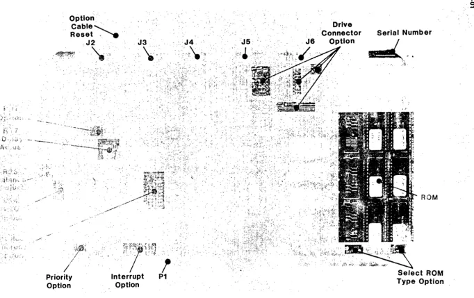
2.01 The Winchester Disk Controller (WDC) 92-1011-xx is an integrated system compo-nent incorporating all the necessary compocompo-nent parts to provide the Mainframe with a single PCA Controller. Figure 2-1 illustrates the WDC. The PCA contains:
(1) A J.l.P section. A dedicated 8-bit J.l.P designed specifically for control applications,
(2) A memory section for storage of the con-trol program and variables,
(3) 796 Bus Interface section to provide for bus arbitration,
(4) Control and Status Register section, (5) Read and Write section,
(6) Phase-Locked Data Recovery section. 2.02 The PCA measures 6.0 inches by 12.0
inches. A pair of edge-type PC connectors, P1 and P2, mate with the 796 Bus backplane connectors.
(1) PI is a dual 43-position, 86-conductor PC connector. The pin assignments conform to the 796 Bus specifications.
(2) P2 is a dual 30-position, 60-conductor PC connector. The pins are vacant and are not used by the bus.
2.03 Five edge-type PC connectors, J2 through J6, provide for the data control and status to control up to four drives.
(1) J2 through J5 are dual 10-position, 20-con-ductor PC connectors. These provide for the data communication between the WDC and each drive. A separate cable is connected to each drive, i.e., star connection.
(2) J6 is a dual 25-position, 50-conductor PC connector. This provides for the status and control signals between the WDC and Drives. A single cable is connected to each drive, i.e., daisy chain connection.
05-0003·01
Options
2.04 Several alternate features can he configured through option jumpers on the PCA. Refer to Figure 2-1.
(1) WI through W8 select the ROM type when WDC is optioned for ROM.
(2) W9 through WI8 configures the disk drive connectors for 8.0-inch or 5.25-inch drive signal locations.
(3) WI9 through W26 select the interrupt level for WDC.
(4) W27 through W28 select WDC for 8- or 16-bit data transfers.
(5) W29 through W44 set the I/O port address. Normally this is 90·97H.
(6) W45 sets WDC to highest bus master priority.
(7) W46 and W47 set the INIT* for master or slave operation.
Adjustments
2.05 Three multi-turn trim potentiometers are provided for adjustments in the analog sections:
(1) R17 sets the delay for the Synch Field Detector.
(2) R23 balances the VCO Error Amplifier. (3) R34 adjusts the VCO frequency.
External Reset Switch
~C:
.
~
.(
IJ.
4k x 24
Fast IV Select Device Decode
----.
----.
• Decodes
•
•
--.
Address ~
Mark Voltage
Detection
~
ControlledOscillator
Read Only
24 'If!
A 8X300 uP <f- 6.67 MHz Oscillator
CRC Generator
And - .
Write Precomp
J---~
~-Memory 11 13
t
2Decode ~
8
RESET* Power
On W46 \.
Reset ~
INIT
,
796 Bus Interface
~
P1 '
,
To 796 Bus
Check
r---...&-_t..,. ,...-.
t __
Serial To Parallel Converter
IV Bus
8
"
6k x 8 RandomAccess Memory
Parallel To Serial Converter
3. FUNCTIONAL DESCRIPTION
3.01 The basic function of a disk drive controller is to provide dedicated electronics for con-trol and positioning of the drive read/write head(s) and the logic for read/write operations.
Disk Storage
3.02 The Winchester Disk Controller (WDC) stores random access data and program files on two non-removable 5.25-inch disks. Each of these disk surfaces employs one movable head to service 153 data tracks. The media is made up of a rigid aluminum disk substrate coated on both sides with ferrous oxide similar to that found on audio tape. Read/write head(s) do not come into physical contact with the media.
3.03 Low . cost and high drive reliability are achieved through the use of a band actuator and an open loop stepper motor positioned head. Refer to the OEM Disk Drive Technical Manual for a detailed functional description.
3.04 Formatting the disk divides the media read/write area into logically numbered tracks. Individual tracks are further subdivided into logical sectors. Each sector is 128 Bytes with 38,144 sectors per drive. Sector locations are determined logically and termed Soft Sectored. Information is stored on both surfaces of the disk(s). A single disk index position is monitored by the drive status logic. This logic issues an INDEX * pulse to the WDC each time the disk starts a new revolution. The computer Operating System uses the logical sector location and the indexing information to randomly access the stored files.
Overview
3.05 Figure 3-1 illustrates the principal sections of the WDC in block diagram. This figure and Figures 3-2 through 3-6 should be used in conjunction with the WOC logic diagram for the descriptions which follow.
3.06 Direct Memory Access (DMA) operation is
pf~rformed by the
woe
or Bus Master, as well as, Bu:; slave operation through the use of a uniqup device; a 8X300 mil:roprocpssor (pP).This X·Hit pI' is designed for fast control applica-tions, such as, disk controllers. It has a limited in<;tnl('tilJn «t·t fJf "igh~ in:;t!"u:;t!·.J!~ t~'i1"!:.
3.07
05-0003-01
A 6.67 MH: oscillator clocks the pP re-sulting in a 300 ns instruction cycle time.
3.08 A firmware control program is stored in the 4k x 1-1 ROM. Thirteen pP lines ad-dress this ROM and its associated /JeC(Je/e device.
A 16-Bit instruction is returned to the p P and an additional 8-Bits are appended to the instruction used by the Fast IV Select Decode for direct I/O addressing.
3.09 Both the source device, first 4 bits, and the destination device, remaining 4 bits, are specified in the 8 bit word furnished to the Fast IV
Select Decode for data to be transferred over the
8-bit bi-directional IV Bus, IVO*-IV7*. Table 3-1 lists the decoded signals by their functions. This method of device addressing permits greatly increase system speed over conventional p.P design since conventional I/O addressing requires indivi-dual instructions.
3.10 The 8X300 p. P can address a source device, have that device place data on the IV Bus, and this data can then be taken into the pP all in the first half cycle or 150 ns. Data can be pro-cessed by an arithematic function included in the instruction read from ROM and the result placed back on the IV Bus targeted for storage in another device during the second half cycle.
3.11 A RESET* issued from Power-On-Reset causes the p. P to initialize. Activation of
thePower·On-Reset can be through these channels.
(1) Application of power to the +5 Vdc Bus.
(2) An INIT* received from the 796 Bus. Optionally, a INIT* can be issued to the 796 Bus.
3.12 I/O information can be transferred over the IV Bus between a'ny of the WDC devices with or without passing through the p P.
(1) 6k x 8 Rallt/Olfl Access Memory - WDC statu$ and control variables are stored in RAM, e.g., data transferred to or from the 796 Bus.
05-0003-01
Table 3-1 - Fast IV Select Decode Signals
Mnemonic Function
LMBAM* Load 796 Bus Address Middle, AB-AF_
LMBAH* Load 796 Bus Address High, AIO-Al3.
LRAMAL* Load RAM Address Low, RAO-RA7.
LRAMAH* Load RAM Address High, RAB-RAIO and CEO-CE3.
LDCNL* Load Disk Control Register.
LMUX* Load Multiplexer.
LMBD* Load 796 Bus Data, DBO-DB7 or DBB-DBI5.
LFCNL* Load Function Control Register.
LDSKDAT* Load Disk Data Register.
LRAM* Load RAM Data Register.
PTIMER* Pulse Timeout Timer.
PMBACK* Pulse 796 Bus Acknowledge.
MBRD* Pulse 796 Bus Read Request Flip Flop.
PCIDX* Pulse Clear Index Flip Flop.
RMBCMD* Read 796 Bus Command Register.
RRAM* Read RAM Data Register.
RMUX* Read Mux.
RMBD* Read 796 Bus Data Register.
RFCNTL* Read Function Control Register.
.
(3) Reael alld Write Logic - data is transferred between the IV Bus and disk drive(s).
(4) nisk. Status all(1 ('olltrol - contains disk
status buffers and control registers.
(5) Illterrupt - provides for setting WDC
interrupt level.
3.13 The on-card 6k. x 8 RAM stores control variables and data. Addressing of this mem-ory. is controlled by external registers in the form of counters. The J1 P loads these initially with the device decoder.
3.14 The WDC has both 796 Bus Master or slave device attributes.
(1) As a master device the WDC generates requests to the 796 BIIS Illterface for storing and receiving data in other 796 Bus devices.
(2) As a slave device, other 796 Bus Master devices, e.g. CPU, can address the WDC. The on-card RAM is not accessable by 796 Bus devices.
3.15 The most complex portion of the WDC is the Read and Write Logic. Complexity is greatly reduced through the use of a five device set which performs the functions:
(1) The Address Mark Detectioll is used by the WDC to find an ID address mark or data address mark in the serial data stream.
(2) The Serial to Parallel alld Parallel to Serial
COllverters are shift registers used to
con-vert serial data to the parallel IV Bus.
(3) Write serial data has a CRC word calculated and appended for each block of data as it is written to the disk. A check of this CRe word is made for each block of data read. Both of these operations are performed by the CR C Gellera-tioll alld Check.
(4) Write PreC()Ill{leIlSafioll is performed to
data d,';)ending on the disk location which the da:;.l i.;
:u
be written. An individm.l re-cording transition is either made slightly early or late to l:ompen:;aw for bit crowding on the disk. Th" ",rjt(\ d;-tt;l r:lSSPS throu;;h :1.!-::ulti-05-0003-01
plexer associated with a delay line to provide the actual compensation in time. Individual line drivers are used to supply write data to up to four drives due to the high data rate of 5 MHz.
(5) The Voltage COlltrol/e(1 Oscillator is used to develop the read clock. It is referenced to the VCO center frequency when reading is inactive.
3.16 The WDC can generate interrupts to the 796 Bus on any of the eight 796 Bus levels, INTO*-INT7*, through option jumpers. An inter-rupt is used to tell the 796 Bus an WDC operation is completed.
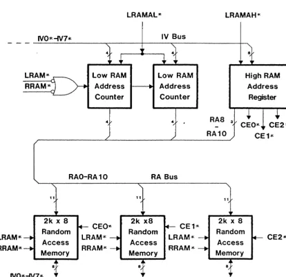
Memory
3.17 Refer to Figure 3-2 for the description which follows. The contents of the 6k x 8
Random Access Memory is exchanged as data to
the IV Bus, IVO*-IV7 *, with one of two instruc-tions:
(1) LRAM* - Load RAM Data Register, (2) RRAM* - Read RAM Data Register.
3.18 The starting RAM address is stored in a counter and a register from the IV Bus with the commands LRAMAL* and LRAMAH* issued by the control program.
(1) The Low RAM Counter stores the least significant 8 bits.
(2) The High RAM Register stores the most significant 3 bits and the chip enables for individual 2k RAM devices.
Both of these form the ll-bit RAM Address Bus, RAO-RA10. This method of addressing provides for performing block data exchanges with memory using a single instruction once the control program initializes them. The Address Couflter is incre-mented at the completion of each read, RRAM*, or write, LRAM*, operati011. This auto-increment-ing feature permits very fast data transfers.
3.19 The High RAJ! .. lrfJress Register is re-loaded, LRAMH*, by t11l' control program when a boundary is crossed, e.g., when the 8-bit
Low RAIH COl/iller migbt overflow. Individual
05·0003·01
LRAM* RRAM*
LRAMAL * LRAMAH *
IVO* -N7* IV Bus
- ~~~~---~~----~---~---~~
..
LRAM* Low RAM
RRAM*~"
Address~
Counter..
..
Low RAM
1----i.M Address
Counter
..
/'
1
High RAM Address
Register
RA8 3
~
+
CEO* CE2*
RA10 CE1*
RAO-RA 1 0 RA Bus
11 11 11
2k x 8 2k x8 2k x 8
Random
f4--
CEO* Random ..- CE1* Random---
Access LRAM* - . AccessLRAM* ___
Access
f4--
CE2*-+
Memory RRAM*
-+
Memory RRAM*-+
Memory8 8
IVO* -N7*
j
[image:10.629.127.542.161.562.2]
by the remaining portion of the A ddress Register
eliminating the need for an individual device decoder.
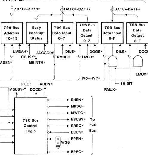
796 Bus Interface
3.20 Refer to Figure 3-3 for the description which follows. The 796 Bus Interface is made up of two subsections.
(1) Data and address registers which commu-nicate with the 796 Address Bus, ADO*-ADI3*, and 796 Data Bus, DATO*-DATF*.
(2) Control signals and logic for timing data transfers with the 796 Bus.
3.21 Signal ADEN* from the 796 Bus Control
Logic gates the 796 Address 0-7. 8-F. and
10-/3 registers on to the 796 Bus. The 796 Address
registers are loaded from the IV Bus, IVO*-IV7*. Fast IV device decodes are supplied to load each register.
(1) LMBAM* to 796 Bus 8-F register, (2) LMBAH* to 796 Bus 10-13 register,
(3) PMBRD* or PMBWR* to 796 Bus Address
0-7 register.
Each time read or write request, PMBRD* or PMBWR*, is made to the 796 Bus COlltrol Logic
the least significant bits of the address are loaded into the pP.
3.22 The pP monitors the 796 Address Bus, ADRO-ADR2, and IOWRDEC during I/O cycles through the 796 Bus Command Gate. if the WDC is idle, the pP checks 10WRDEC. If set, ADRO-ADR3, are checked to determine what to do with the data presented on the 796 Data Bus.
It will interpret this as:
(1 ) The least significant 8 bits of a Command Block Pointer.
(2) The next 8 bits of a Command Block Pointer.
(3) The most significant 8 bits of a Command Block Pointer.
05-0003-01
This operation l)('rforms the function of an address decoder normally performed by firm ware. After this is stored in a pP register, an external acknow-ledge, XACK* is issued completing the 796 I/O cycle. Typically this cycle will be 1.5 ps, because of the fast pP response time.
3.23 796 Bus address lines, ADR3* through ADF*, are input to Address Decode and compared to the Address Optioll ./umper thereby determining the unique 796 Bus device I/O address. The 8 or 16-bit Optioll Jumper determines the address length. The address option jumpers apply to A4-A 7 and AS-AF. For example, if the desired address for 8-bit addressing is 90H, the same strapping would make the 16-bit address 9090H.
3_24 The output of the Address Decoder(s) is a device select to Input Output COlltrol
created from:
(1) 796 Bus I/O Write, IOWC*, or I/O Read, IORC*.
(2) A comparison between the address pre-sented on the 796 Bus and the unique WDC address.
3.25 Illput Output Control performs two func-tions.
(1) On an I/O Read, and I/O Read Decode, IORDDEC, is issued to the Bllsy Illterrupt Status.
(2) On an I/O Write, and I/O Write Decode, IOWDEC, is issued to the 796 Bus
Com-malld Gate.
3.26 The WDC data register is made up of four 8-bit registers.
(1) 796 Blls Data Illput 0-7.
(2) 796 Bus Data IIIPllt 8-F.
The 796 Data Bus is connected to the register inputs and the IV Bus is connectp.d to the> register outputs.
(31 7'16 HilS Data Output 0-7.
( 4) 796 IJ II S Data 0 II {P III 8- F.
05-0003·01
ADECODE~
Address
Jumper
Option
/
8
A
..
5
Address
Decode
Address
Decode
~~
t
t
8 or
16-Bit
Option
Jumper
8
ADRO*-ADR7*
,It'ADR8*
I'.
~OWRDEC
8,ADRF*
3
8~
+
P---~
r---,
796 Bus
Address
0-7
i
ADEN*
8 ,
796 Bus
Command
Gate
796 Bus
Address
8-F
i
~~
i
4
ADEN* 1MBAM*
~
,
B
.... - - - -
- - - _ _ _
-+-_-+-~...:..::.IVQ*-IV7*
_
__=_=~ _ __L~+_-~C---L----/
r
IOWC*~
IORC *
---<;L---I ___
--
~
IOWRDEC IORDDEC
t
t
Input
~
Output
Control
To
796
Bus
I
AACK*.-- -
---~XACK*
16 BIT
1-MRESET*
--;-PMBRD*
tPMBWR* .
-~,
XACK*
XACK*.,---~~---~---~ ~
Interrupt
-"'" y
MBINTR*
Priority
Options
•
_.
y
Jumper
W19-W26
~y
-Fiqure 3-3 - 796 Bus Interface Block Diagram
INTO*-l
INT1*
INT2* To
INT3* 796
INT4* Bus
INT5*
I
INT6*
j
INT7*
-05-0003·01
- To 796 Bus - - - -______________________
"
/['- AD 1 O*-AD 13*
4
/
796 Bus
Address
10-13
Busy
Interrupt
Status
t
796 Bus
Data Input
0-7
~
i
4~1MBAH*
ADGCODE
4~
i
DllE*
ADEN*
CBUSY~,
MBINTR*
8
RMBD*
796 Bus
Data
Output
0-7
~
i
DOOE*
8
1MBD*
:-8
DAT8*-DATF*
796 Bus
Data Input
8-F
i
DllE*
8f-'r
796 Bus
Data
Output
8-F
I
I
i
DOOE*
I
lMUX*
/ /
/ IVO*-IV 7* /
DllE*
ADEN*
-MBUSY*~
DOOE*
4~..
...
..
t
t
796 Bus
Control
logic
h
h
~---~~
r--..
..
..
...
..
..
_
...
...
W25
...
BHEN*
MRDC*
MWTC*
BBUSY*
BREa*
BClK*
BPRN*
BPRO*
To
796
Bus
' - 16 BIT
RMUX*
[image:13.621.62.559.79.629.2]05-0003-01
3_27 In the OMA mode, the loading and reading of these registers is in part under control of the 796 COlltrol Logic.
(1) DILE* - Data Input Load Enable,
(2) DOOE* - Data Output Output Enable,
To load data from the 796 Bus into the 796 Blls
Input register DILE* is asserted. Data is sent to the
796 Bus from the 796 Bus OllfoUf register when DOOE* is asserted. Both of these signals apply to the external side of the WOC and are dependent on the direction or transfer of data.
3.28 On the internal side, Fast IV select decode signals handle loading and reading of these registers to IV Bus.
(1) RMBD*
(2) LMBO*
Read 796 Bus Dala Register.
Load 796 Bus Data Register.
(3) RMUX* - Read Multiplexer.
(4) LMUX* - Load Multiplexer.
Table 3-2 - Winchester Disk Controller Active 796 Bus Signals
Diagram 796 Bus
Mnemonic Mnemonic (1) Pin Function
BCLK* BCLK* 13 Bus Clock_
MBINIT* INIT* 14 Initialize_
BPRN* BPRN* 15 Bus Priority In_
BPRO* BPRO* 16 Bus Priority Out.
•
BBUSY* BUSY* 17 Bus Busy.
BREQ* BREQ* 18 Bus Request_
MRDC* MRDC* 19 Memory Read Command_
MWTC* MWTC* 20 Memory Write Command.
IORC* IORC* 21 I/O Read Command.
-IOWC* IOWC* 22 I/O Write Command.
XACK* XACK* 23 Xfer Acknowledge:
AACK* LOCK* 25 Lock.
BHEN* BHEN* 27 Byte High Enable.
INTO*-INT7 * INTO*-INT7 * 35-42 Parallel Interrupt Requests.
AO*-A13* ADRO* Various 20-Bit Address Bus.
OBO*-DBF* DATO*-DATF* Various I6-Bit Data Bus.
Note:
(1) Addr~ss and data bus lines are In hexadecimal notation.
3.29
(1) (2) (3) (4) (5) (6)
(7)
(8)
The 796 Bus Control Logic "'exchanges the
796 Bus arbitration signals.
BHEN*, MRDC*, MWTC*, BBUSY*, BREQ*, BCLK*, BPRN*, BPRO*,
The functions of each are described in Table 3-2. Option Jumper, W25, provides for making the WDC highest priority Bus Master.
3.30 On the other side of the 796 Bus Control
Logic are the signals generated on the WDC
or used to control the 796 Bus signals.
(1) 16 BIT - defines whether the WDC is transferring 8- or I6-bit words to the 796 Bus.
(2) MRESET* - is the WDC reset.
(3) PMBRD* - a Fast IV Select Decode signal. (4) PMBWR * - a Fast IV Select Decode signal. When (3) or (4) are strobed, the 796 Bus Control
Logic initiates the 796 Bus handshaking, and
transfers the data. During the transfer, the J.lp
checks:
(5) MBUSY* - 796 Bus Busy over the IV Bus to determine when ~he transfer is com-pleted.
3.31 Option Jumpers, WI6-W26, set the
Inter-rupt Priority for MBINTR* to the 796 Bus
Interrupt Levels, INTO*-INT7*. MBINTR* is gen-erated by the J.lP over the IV Bus at the end of a . data transfer.
3.32
05-0003-01
The transfer acknowledge, XACK*, has two possihle directions.
(1) This signal is created on the WDC and sent to the 796 Bus in response to an I/O read or write.
(2) This signal is input to the WDC from the 796 Bus at the completion of a data tran-fer from another Bus Master.
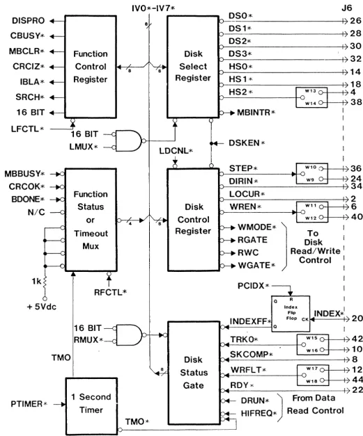
Control and Status
3.33 Figure 3-4 illustrates the internal WDC status and control registers and transfer gates in block diagram. The Disk Select Register,
Disk Control Register, and Disk Status Gate
connect directly to the Winchester Drive by the disk status and control cable.
3.34 Option Jumpers, WI3-W1S, provide for alternate, J6, wiring to accommodate two different Winchester disk drives.
(1) Seagate Technology 506. The 506 uses a 34-conductor connector.
(2) Shugart Associates 1000. The 1000 uses a 50-conductor connector.
3.35 The Disk Select and Control Registers are enabled with DSKEN*. This provision is made to prevent invalid write operation to the disk drive before the J.lP sets up the initial values in the registers, e.g., during power on operation. The Disk Select Register determines which drive and surface is accessed.
(1) DSO*-DS3* are the drive select lines for up to four drives. Only one of these are assert-ed at a time.
(2) HSO*-HS2* are coded head select lines for up to 8 heads.
The remammg register output is used internally to the WDC.
05-0003-01
0 . .
-DISPR
CBUSY
MBCLR
* .
-*
..-*
+-*
*
..-CRCIZ
IBLA
SRCH
16 BI
T+-LFCTL *
*
-.c
MBBUSY
CRCOK
BOONE
N/C
*
-.c
*
-.c
--c
-
...r ~ ~ ~1k
(Function
Control
Register
~
16 BIT -c
LMUX* -c
Function
Status
or
hI'-'
Timeout
Mux
,~
t
~v
~SO*
h
DS1*
I'-'
DS2*
h
Disk
hOS3*
, /~
Select
HSO*
8 h.
Register
h
HS1 *
h
HS2*
I'-'
p..-.
MBINTR*
(:Y
-h
,... ~
OSKEN*
LDCNL*
*
')h
STEP*
h
DIRIN*
h
LOCUR*
:-'
Disk
hWREN*
/
..
/~
Control
I'-'4 ..
p.-..WMODE*
Register
b--+RGATE
b--+RWC
p.-..
WGATE*
,
W13 ().
W14(}.
Wl0 (\ ~
-
.
W9 n
W110
..
-.
W120To
Disk
J6
26
28
30
32
14
18
4
11 " ' ; " I) " ' / " 1 / " ,/ 1 1 1 1 1 1 " ' / ',
:-( T7 ":(
T7 " C7 1 i38
36
24
34
2
6
40
Read/Write
IControl
II I
RFCTL*
PCIDX*~ I+5V dc
16 BIT-c
RMUX*---c
TMO
1 Second
PTIMER*
--Timer
~
....'-Disk
~
Status
Gate
TMO*
h
I'"'
a R
Index
Flip
h...LINDEXFF*
FlopI'--' a
-h...
TRKO*
.
h.LSKCOMP*
.... ~WRFLT* 1'-''''h.LRDY ",
.... I IINDEX*"
CK :-'" T7
20
W15 ().
W16 ().
W170
W180
I
" C7
J71
42
o
8
2
44
22
',
C781
" T7 ,,-17p.-
DRUN*
J
From Data
~
HIFREQ* Read Control
[image:16.615.57.578.61.687.2]3.36 Head position and write control informa-tion are determinC'd by the value in the
J)isk COl/trol Register.
(1 ) STEP* moves the head one increment. (2) DlRIN* determines the direction of the
hC'ad movement.
(3) LOCUR * is a control signal furnished to the drive to reduce the write current on different tracks. These tracks vary for different drive types. This line allows the control
pro-gram to adjust the current when appropriate. (4) WREN* is the write enable signal to the
drive.
The four remaining lines are supplied to the Disk Read Write Control. Refer to Figure 3-5.
(5) WMODE* sets the Read/Write logic to Write Mode.
(6) RGATE* sets the Read/Write logic to Read Mode.
(7) RWC* is Reduce Write Current and means to internally perform write precompensa-tion in the Read/Write logic.
(8) WGATE* is the Write Gate or data. LDCNL* from the Fast IV Select Decode fur-nishes the control for this register.
3.37 Current disk status information is gated onto the IV Bus, IVO*-IV7*, through the
Disk Status Gate.
(1) IND EX
*
is a short duration pulse furn-ished by the drive at the start of each disk revolution. The II/dex Flip Flop functions as a storage register and is cleared by the control program with Fast IV Select Decode PCIDX*.(2) TRKO* indicates the drive heads are posi-tioned at Track 0, the lateral indexing location on the disk.
(3) SKCOMP* is the Seek Complete signal. (-i) Vdo: U' i: i::; the Writ" Fault signal.
(5) RDY* is the disk drive Ready signal.
05-0003-01
The three remammg status signals are generated within the WDC.
(6) DRUN* indicates the Synch Field Detector has detected a field of all zero's. This is the synch field before the Address Mark.
(7) HlFREQ* indicates the Address Mark De-tector has detected a high frequency field. This is a 5 MHz signal which may be an all zero's pattern. The all zero '5 pattern is the bitsynch
field preceeding an ID Address Mark or a Data Address Mar k.
(8) TMO* indicates the data transfer was abortive and must be restarted.
3.38 The FUI/ction Status or Timeout
Multi-plexer monitors the WDC status lines:
(1) MBBUSY* is the signal furnished from the
796 COl/trol Logic indicating the 796 Bus
is performing a data transfer.
(2) CRCOK* is the signal furnished from the Read and Write logic indicating that the CRC check was made.
(3) BDONE* is the signal furnished from the Read and Write logic indicating serial to parallel conversion was performed.
The control program cannot interleave the status-ing of these lines within every data transfer opera-tion and maintain high speed operaopera-tion. At the start of transfer the control program asserts Fast IV Select Decode PTIMER * starting the 1 Second Tim er. Should any of lines (1), (2) or (3) above not go high in 1 second, the WDC control program considers the operl1tion abortive. The WDC logic must be cleared and the operation restarted. After one second TMO* forces the outputs high and asserts TMO* to the Disk Status Gate. At the completion of each transfer, the control program checks TMO*. If a time out has decoded, it asserts RFCTL* and checks the FIII/ction Statlls to determine which input caused the aborted opera-tion and then restarts the data transfer.
3.39 The Functiol1 CUlltrol Register outputs are used withill Lht! WDC.
05·0003·01
RCLK RCLK* RDAT* CLKS* DRUN
Address Mark Detector
RDSKDAT*
Serial To IVO*-IV7* Parallel
8 Converter
WMODE*
SRCH HIFREQ AMDET*
BOONE DOUT
SELD
Read Data Demux
ASEL*
W----~=__B J2.1
/h.:...:.::...:=-~ J2.17
M--< J2.18
H---==_=_~ J3.1
/1'"'1_-~ J3.17
14--<
J3.18H - - - = = ' - B J4.1
..-'h.=..:....:::::::--~ J4.17
[image:18.618.63.565.143.605.2]14--< J4.18
...
----==~-t7 JS.1/r>=-=--':=--+-> JS. 1 7 14--< JS.18
'----_...I
LD SKDAT*
CRCIZ* CRCOK*
Parallel
To DOUT
Serial
a...;. _ _ _ ...1 BOONE
Delay
WCLK* Line
CRC Generator
And Check
I
WCLK
DIN*
NRZD*
TIMCLK
RWC DL YDAT WGATE
MFM Encoder
NOM LATE EARLY
WCLK WCLK*
Mux
Figure 3·5 - Read and Write Logic Block Diagram
WRDATA
0 - - - - l - ' > J2.14 J3.14 ~---l4 J2.13 J3.13
" " , " - - + ' ; J4.14 JS.14
'---/ J4. 13 JS.13
0 - - - - l - ' > J2. 1 0 J3. 1 0 ~-~ J2.9 J3.9
(2) CBUSY* indicates the controller is busy and is USl'cl hy tlH' Busy Interrupt Status. (3) MBCLR * genNutps a 796 Bus INIT* and will initialize the Bus if Option Jumper W47 is installed.
(4) CRCIZ* initializes the CRC Generation and Check. Refer to Figure 3-5.
(5) IB LA * generates an Address Mark.
(6) SRCH* initiates a search for an Address Mark in the read data. Refer to Figure 3-5. (7) 16 BIT indicates a 16 bit data transfer.
Read and Write Logic
3.40 Refer to Figure 3-5 for the description which follows. The Read and Write Logic perform the function of MFM Generation and Decode.
3.41 In the Read Mode, the first operation to perform is to locate the Address Mark in the Read data, so the preamble can be checked for addressed sector and cylinder number. The Address
Mark Detector has four signals from the
Phase-Locked Data Recovery input to it.
(1) RCLK and RCLK* are the Read Clock generated by the VCO.
(2) RDAT* is the Read Data and is synch-ronized to the VCO. A RDAT* transition indicates a data transition.
(3) CLKS* is the signal clock. CLKS* indicates a clock transition.
(4) DRUN* indicates the Synch Field Detector has detected a field of all zero's. This is the synch field before the Address Mark.
3.42 The pP uses two signals to control and monitor the Address Mark Defec/or.
(1) SRCH * initiates a search for an Address Mark in the read data.
(2) HfFREQ* indicates the A ddress Mark
De-tector has detected a high frequency field.
This is a 5 MHz signal which mayor may not
hp all zero's.
05·0003·01
When the A(lclre.H Mark fJeteclor deleds the Address Mark, AMDET* is ass\~rtC'cl to the Serial to Parallel COl/perler.
3.43 RCLK* and RDAT* are both uSl'd as inputs to the Snial III Parallel COIII'erln.
Read Data is shifted into an internal shift register until an 8-bit word has been assembled. The converter then asserts BDONE.
(1) BDONE at this time indicates to the pP that a word has been assembled and been transferred to a separate internal buffer register. This provides the J.1P with one word time to read the assembled word onto the IV Bus and clear BDONE.
The Fast IV Select Decode asserts RDSKDAT* to gate this word onto the IV Bus and clear BDONE.
3.44 The last operation performed in the Read Mode is to make a CRC check on the Preamble and the Read Data words. RCLK * clocks these words through the CRC Gel/erator
ol/d Check. If the check is determined to be
correct:
(1) CRCOK * is asserted to the Disk Status Gate.
(2) CRCIZ* is issued from the Function Con-trol Register to clear out the CR C
Genera-tor alld Check before it is used again.
3.45 In the Write Mode, the first operation to perform is a Read Mode operation until the addressed sector is located. A switch is made at the end of the Preamble to the Write Mode by asserting WMODE*.
3.46 LDSKDAT* loads the 8-bit Write Data word from the IV' Bus into an internal register of the Parallel III Serial COI/I'erter. The Write Data word is shifted out as serial data, DOUT*, and on to DIN* of the CR C Gel/era/or
alld Check. The clocking is performed by WCLK*.
3.47 A CRC word is cakulatpu from and appended to the Write Data. Output data:
05-0003-01
' - - ' E ---+ Synch
T---+ Field RGAT
MRESE
SEl D - .. Detector
Start In Ph •••
Synch Field
Detected
Delayed
SRC H
~
Synch Field
Detected
.t
,
Phase
~ MUX
-.
Detector
110
MHzWrite ~ WClK (5 MHz) Clock
--+
WClK*t
20 MHz
DLYDAT
1
...
SRCH
Start In Ph ••• Control
Up
Error 10 MHz
~
Amplifier Voltage And
,.
ControlledDown
~ Filter Oscillator
f
f
R23 R34
Balance Osillator Adjust
Analog +5 Vdc
~
+5VdcCrystal +12Vdc -- Regulator
-12 Vdc --.
1 SHOT
•
DRUN*
r
DRUN DlYDAT r
RDAT*
Data Or
...
Clock
Detector ClKS* RClK RClK*
--+
Derive 1---<1-+ Clock Phasing
-5 Vdc - . Analog
Regulator -5Vdc
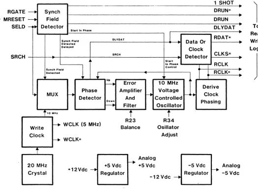
-Figure 3-6 - Phase-Locked Data Recovery Block Diagram
l
To Read Write logic
[image:20.620.58.584.197.583.2]3.48 Tht> M FM Ellcodu pt'rforms two opera-tions to the Write Data.
(1) TIll' Write Data is converted from NRZ format to a M FM encoded signal.
(2) The Encoder provides the control lines NOMINAL, LATE or EARLY for the write precompensation. A particular write tran-sition will be held at its true potran-sition which falls on either a data or clock transition, if the NOMINAL line is selected. If the LATE line is selected, the write transition will shift 12 ns after the true position, or if the EARLY line is selected, the shift will be 12 ns before the true position. The true position is referenced to the WCLK
*
transition.3.49 A Delay Line furnishes the delay outputs to the Multiplexer.
(1) Early is a 24 ns delay.
(2) Nominal is a 36 ns delay.
(3) Late is a 48 ns delay.
3.50 Write precompensation is necessary when the disk has bit crowding. Bit crowding is caused by higher bit densities in sectors toward the center of the disk. Exact cylinder positions to begin with precompensation depend on the disk drive type. For this reason, exact cylinder locations for write precompensation are provided in the control program. Write precompensation has the effect of restoring the phase relationship in the Read Data during data recovery.
3.51 Two control lines are input to the M FM Encoder.
(1) RWC activates write precompensation to the Write Data. RWC is not asserted in those sectors of the disk which do not have bit crowding.
(2) DLYDAT is generated in the Read Data Phase Detector. It is the Write Clock delayed by 60 ns.
3.52 WRDATA, the Write Da~a uu~put line, is distributed through two differential line drivers to up to four disk drives. Each drive has a
OS-0003-01
separate disk data connectors, J2-J5. Additionally, TIMCLK, Time Clock, a general purpose reference frequency required by some drive types, is also distributed from these disk data connectors.
3.53 MFM Encoded Read Data is input to four differential receivers connected to the disk data connectors as lines:
(1) ARD*/ARD.
(2) BRD*/BRO.
(3) CRD*/CRD.
(4) DRD*/DRD.
Note each differential line has an associated select line, A/B/C or DSEL*. Incorrect cable connections
between the disk drives and the WDC are elimina-ted through a unique design. The select line from the accessed disk drive is asserted by the drive. The
Read Data Multiplexer then connects its input to
the associated receiver. SELD, Selected Data, is output to the Phase-Locked Data Recovery.
Phase-Locked Data Recovery
3.54 Figure 3-6 illustrates the Phase-Locked Data Recovery in block diagram for the description which follows. Initially, the MFM encoded Selected Data Line, SELD, is input to the
Synch Field Detector which looks for a series of
zero's proceeding an Address or Data Mark. Since this same pattern can also appear in a normal data field, the pP causes the detector to read the incoming data for a preset interval until it does or does not read an Address Mark.
3.55 Once a synch field is detected, the
Multi-plexer is switched by the Synch Field
Detected line. The Multiplexer has two inputs.
(1) A 10 MHz reference from the Write
Clock is initially connected to the Phase
Detector to develop DLYDAT for Write Mode.
(2) When a potential synch field is detected,
the Multilllexer switches to SELD as the
05·0003·01
3.56 The Phasp·Lock loop is made up of three sections.
(1) The Phase /)etector which produces an error signal derived from a phase compari· son of Read Data and the 10 MHz output of the
Voltage Control/ell Oscillator (VCO).
(2) The error signals, Up and Down, are filtered in the Error Am [JIi/ier alld Filter to provide the proper loop response.
(3) The 10 MHz Voltage COlltro/led Oscillator
is adjusted in frequency by the error signal.
The VCO output is phase·locked to the incoming Read Data.
3.57 The purpose of the Derived Clock Phasing
is to produce a 5 MHz Read Clock, RCLK/RCLK*, which is in half bit synchroniza· tion with the incoming Read Data.
3.58 The DLYDAT line derived in the Phase
Detector is input to the Data or Clock
Detector and output to the Read Write Logic for
the Write Mode. RCLK/RCLK* is input to the
Data or Clock Detector as a reference. The
outputs are:
(1) RDAT* is the Read Data. A transition indicates Read Data.
(2) CLKS* is the Signal Clock. A transition indicates a clock.
3.59 A second input to the Data or Clock
Detector is search, SRCH, a control line
from the /JP. Once a possible synch field has been located and the VCO is locked onto the Read Data, SRCH is asserted. This causes the Data or
Clock Detector to start generating data for the
Read Logic.
3.60 The J.l.P monitors DRUN* to determine when a possible synch field has been detected, phase locked and acquiring data. A built in delay is provided in the control program to allow for the phase lock to take place before the J.l.P asserts SRCH.
3.61 Exceptionally fast aquisition time is pro· vided by the Start in Phase line from the
SYllcll Fieltl Detector. The phase lock does not
have to go through a long initialization period since the VCO is started in phase. The oscillator is actually stopped and restarted again to assure proper phasing. There is some phase delay be· tween the VCO and the Read Data immediately after starting the oscillator. For this reason, a delay of about 1 ns is built into the control pro-gram to allow for the phase lock to take place.
3.62 The status line, ONE SHOT, is used by the
J.l.P to determine if the SYllcll Field Detect·
or is still in a possible synch field. A One Shot is held retriggered while a 5 MHz signal is detected, as soon as it becomes untriggered, the bounds of a possible synch field have been exceeded. In this case, the J.l.P restarts the phase lock procedure by looking for a synch field. The trigger is set for 270 ns or 1.5 clock times.
3.63 The criteria for a valid synch field are: (1) The ONE SHOT is retriggered.
(2) 16 hits of all zero's counted by the Synch
05-0003-01
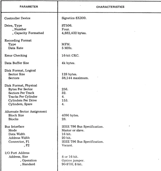
4. SPECIFICATIONS
4.01 Tht.' following furnishes till' user with
if they are performed. Minor deviations from the specifications tabulated in Table 4-1 which do not affect the Winchester Disk Controller performance are excluded from the Codata Systems Corp. warranty.
information for shipping and installation and should be lIsl'd to establish acceptance criteria
Table 4-1 - Winchester Disk Controller 92-1011-xx Specifications
PARAMETER
Controller Device Drive, Type
, Number
, Capacity Formatted Recording Format
Type Data Rate Error Checking Data Buffer Size Disk Format, Logical
Sector Size Sectors
Disk Format, Physical Bytes Per Sector Sectors Per Track Tracks Per Cylinder Cylinders Per Drive Cylinders, Spare
Alternate Sector Assignment Block Size
Blocks Bus Interface
Mode Data Width Address Width Connector, P1 , P2 I/O Port Address Address, Size
, Operation , Standard
Signetics 8X300. ST506.
Four.
4,882,432 bytes.
MFM. 5 MHz. I6-bit CRC. 4k bytes.
128 bytes.
38,144 maximum.
256. 32. 4. 153. 4.
4096 bytes. 28.
CHARACTER ISTICS
IEEE 796 Bus Specification. Master or slave.
16 bit. 20 bit.
IEEE 796 Bus Specification. Vacant.
[image:23.623.44.562.165.718.2]u:")-\)003·0 1
Table 4-1 - Winchester Disk Controller 92·1 011·xx Specifications (Continued)
PARAMETER CHARACTERISTICS
Interrupt
Operation Option jumper.
Type Level.
Levels Eight.
Reset
796 Bus INIT* Option jumper; master or slave. External Switch contact closure optional.
PCA Dimensions IEEE 796 Bus Specification. Length 30.5 cm (12.0 inch).
Width 17.1 cm (6.75 inch). Spacing 1.3 cm (0.5 inch).
Input Output Connector, J2-J5 20-conductor; mates to Ansley 609-2015M. , J6 50-conductor; mates to Ansley 609-5015M.
Environment Temperature
Operating 4 C to 55 C (32 F to 131 F). Storage OCto 65 C (32 F to 149 F). Humidity 5% to 90%, noncondensing.
Power Requirements
+12 Vdc Bus 0.5 A. +5 Vdc Bus 2.5 A. -12 Vdc Bus 0.5 A.
Weight 397 g. (14.0 oz.).
5. OPERATION AND PROGRAMMING Options
5.01 Before the Winchester Disk Controller WOC is installed into the Mainframe card cage, the PCA options should be verified.
(1) Check the WI through W47 Option Jump-ers. Refer to Table 5-1.
(2) Check U30, U31, U48, U49, U76, and U77 ROM. Refer to Table 5-1.
5.02 Install the PCA into card position designa-ted for the WDC. Refer to the Mainframe Hardware Reference Manual. Connect the disk I/O cables to J1 through J6.
Controller Programming - General
5.03 Disk commands and addressing parameters are sent to the WDC by a Command Parameter Block (CPB) located in system RAM. The pointer to the CPB address is sent to the WDC by a series of bytes output via I/O ports.
5.04 The CPB contains information defining two other blocks of system RAM, the Data Block and a Status Block. A typical command sequence is:
(1) Read I/O port WDCBASE+O and wait until the WDC is not busy.
(2) Set up the CPB in system RAM for the next operation.
(3) Issue the pointer to the CPB using I/O writes to WDCBASE+O, WDCBASE+2, and WDCBASE+4 in that order.
(4) Start the controller by issuingWDCBASE+6. If not operating under interrupts, wait until:
(5) The WDC is not busy by reading I/O port WDCBASE+O until the busy bit is reset.
05·0003·01
(6) Check the status of the last operation by referring to the status block in system RAM.
If operating under interrupts:
(7) Return to normal processing until an interrupt from the WDC occurs.
(8) When the interrupt has occurred, check that the interrupt was caused by this de· vice by reading I/O port WDCBASE+O and inspecting the interrupt bit. If this device caused the interrupt, clear the interrupt by issuing a write to I/O port WDCBASE+7 to clear the interrupt.
(9) Determine the status of the last operation by referring to the status block in system RAM.
I/O Ports - CPB Pointer
5.05 Eight Consecutive I/O port addresses are used by the WDC to provide the following control information described below. The base address of the block WDCBASE is set by option jumpers. Table 5-2 tabulates these I/O port address assignments.
5.06 WDC Busy and Interrupt Status - The
byte read at WDCBASE+O represents the following:
(1) Bit 7 WDC Busy. If set, the WDC is busy with an operation. If reset, the WDC may accept a new command.
(2) Bit 6 WDC Interrupting. If set, the WDC is currently interrupting at the priority level set by option jumpers.
(3) Bits 5-0 are not assigned.
5.07 CPIJ Address - The 20-bit address formed
05-0003-01
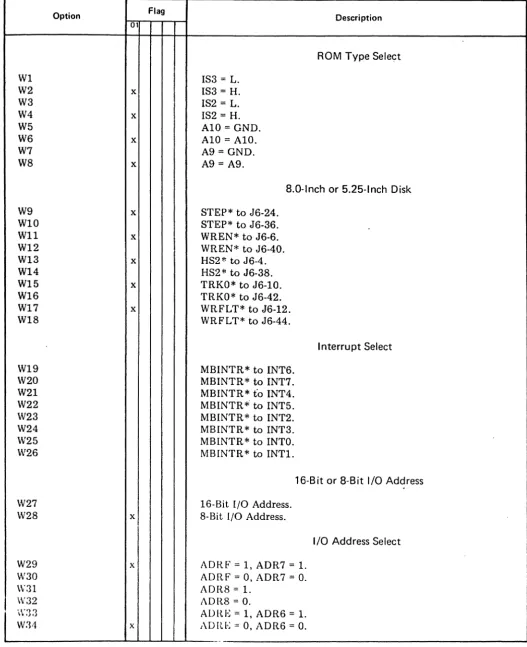
Table 5-1 - Winchester Disk Controller Options - PIN 92-1011-xx
Option
01
Flag
Description
ROM Type Sele<;:t
WI IS3
=
L_W2 x IS3
=
H.W3 IS2
=
L.W4 x IS2
=
H.W5 AIO
=
GND.W6 x AIO
=
AIO.W7 A9
=
GND.W8 x A9
=
A9.S.O-Inch or 5.25-lnch Disk
W9 x STEP* to J6-24.
WIO STEP* to J6-36.
Wll x WREN* to J6-6.
WI2 WREN* to J6-40.
WI3 x HS2* to J6-4.
WI4 HS2* to J6-38.
WI5 x TRKO* to J6-IO.
WI6 TRKO* to J6-42_
WI7 x WRFLT* to J6-I2.
Wl8 WRFLT* to J6-44.
Interrupt Select
WI9 MBINTR * to INT6_
W20 MBINTR * to INT7.
W21 MBINTR * to INT4.
W22 MBINTR'" to INT5.
W23 MBINTR * to INT2.
W24 MBINTR * to INT3.
W25 MBINTR * to INTO.
W26 MBINTR* to INTI.
16-Bit or S-Bit I/O Address
-W27 16-Bit I/O Address.
W28 x 8-Bit I/O Address.
I/O Address Select
W29 x ADRF
=
1, ADR7=
l.W30 ADRF = 0, ADR7
=
O.W31 ADR8
=
I.W32 ADR8 = O.
W33 ADH.E
=
1, ADR6 = l.W:J4 x ADRE
=
0, ADR6 = O. [image:26.617.53.581.78.725.2]--05·0003·01
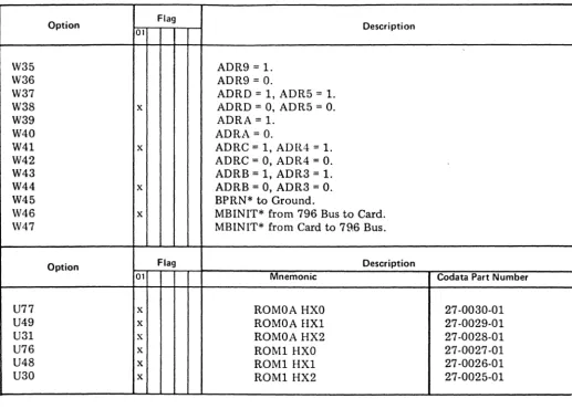
Table 5·1 - Winchester Disk Controller Options - PIN 92·1011·xx (Continued)
Option Flag Description
01
!
W35 ADR9
=
l. IW36 ADR9
=
O.W37 ADRD
=
1, ADR5 = l.W38 x ADRD
=
0, ADR5=
O.W39 ADRA
=
l.W40 ADRA
=
O.W41 x ADRC
=
1, ADHA = l.W42 ADRC
=
0, ADR4=
O.W43 ADRB
=
1, ADR3=
l.W44 x ADRB
=
0, ADR3=
O.W45 BPRN* to Ground.
W46 x MBINIT* from 796 Bus to Card.
W47 MBINIT* from Card to 79.6 Bus.
Option Flag Description
01 Mnemonic Codata Part Number
U77 x ROMOA HXO 27·0030·01
U49 x ROMOA HX1 27·0029·01
U31 x ROMOA HX2 27·0028·01
U76 x RaMI HXO 27·0027·01
U48 x RaMI HX1 27·0026·01
U30 x RaMI HX2 27·0025·01
Notes:
[image:27.620.34.552.76.446.2](1) An X in the Flag column indicates a jumper is installed. a wrapped wire is installed. the switch is set or the ROM is installed.
Table 5·2 - I/O Port Address Assignments
Address Type Function
WDCBASE+O Read WDC Busy and Interrupt Status. WDCBASE+O Write CPB Address Bits 0--7.
WDCBASE+2 Write CPB Address Bits 8-15. WDCBASE+4 Write CPB Address Bits 16-19.
WDCBASE+6 Write WDe Configuration Parameters and GO. i
05·0003·01
5.08 WDC Configuration and GO - Issuing
this byte performs two functions. Certain configuration parameters of the WDC are defined and the WOC is commanded to GO. This byte should be issued only after the CPB has been defined in system RAM, and all three bytes of the CPB pointer have been output. The meaning of the configuration portion of this byte are:
(1) Bit 7 Interrupt Enable. If set an interrupt will be generated at the end of the current operation. If reset no interrupt will be issued.
(2) Bit 6 Data Word Length. If set the Data Word Length is 16 bits. If reset the Data Word Length is 8 bits.
(3) Bits 5-0 are not assigned.
5.09 Reset WDC Interrupt - Issuing an I/O
write to this port causes the Interrupt from the WDC to be reset. In addition, the interrupt status, Bit 6, of WDCBASE+O Read will be reset.
Command Parameter Block
5.10 The CPB organization is listed in Table 5-3.
The Command Byte code description is
listed in Table 5-4.
Table 5·3 - Command Parameter Address Block Assignments
location Description
CPB+O Command Byte. CPB+l Unit Number.
CPB+2 Logical Sector Number Bits 0·7. CPB+3 Logical Sector Number Bits 8-15. CPB+4 Logical Sector Number Bits 16-23. CPB+5 Byte of 00 (1)
CPB+6 Byte Count Bits 0-7. CPB+7 Byte Count Bits 8-15. CPB+8 System RAM Address Bits 0·7. CPB+9 System RAM Address Bits 8·15. CPB+10 System RAM Address Bits 16-19. CPB+ll Byte of 00 (1)
CPB+12 Status Block Pointer Bits 0·7. CPB+13 Status Block Pointer Bits 8·15. CPB+14 Status Block Pointer Bits 16·19. CPB+15 Byte of 00 (1)
Nut .. :
(I) Reserved (ur expansiun.
5.11 Unit Numbl'r - This defines the logical unit number of the disk drive. Option jumpers on each drive define the individual disk. The allowed range of unit is 0 to 3.
5.12 Logical S('ctor Number (LSN) - Refers to the 128 hyte logical sector used to address the disk. The range of addressing is 0 to 094FFH.
5.13 Ilyle Count - Refers to the number of bytes to be transferred. If a count is given which when taken with the System RAM Address exceeds the currently defined 64k Bank, transfer will continue into the next bank.
5.14 If a byte count is given which whel?- taken with the LSN, exceeds the capacity of the drive, an error flag will be returned.
IMPORTANT
If all odd byte COUllt is specified, tlze COlltrol/er will transfer data ill an 8·bit word lellgth evell if a word lellgth of 16 bits was specified ill the data sent to I/O port
WDCBASE+5.
5.15 System RAM Address - The System RAM Address defined in the CPB consists of a 16-bit RAM address and a 4-bit bank address. If the address speCified does not exist, then MBTMO, 796 Bus TIMEOUT, status will be returned.
IMPORTANT
If the starting address specified is an odd address, DMA data transfers will be perform-ed Oil a 8-bit basis evtll if the word length
was defilled to be 16 bit.
The WOC uses the INTEL (R) convention of byte addressing when usink 16-bit memory ad-dressing;
(1) Least significant byte is an even address.
[image:28.613.56.301.435.716.2]OS·0003·01
Table 5·4 - Command Byte Code
Code Description
OOH Return st.atus of specified drive.
0IH Seek/Read.
02H Close Buffer.
03H Close Buffer then verify after write is complete. 04H Not assigned.
05H Format Disk.
06H Surface Analysis.
07H Restart WDC.
OSH Reserved for diagnostic operation code. 09H Reserved for diagnostic operation code. OAH Reserved for diagnostic operation code. OBH Reserved for diagnostic operation code. OCH Reserved for diagnostic operation code. ODH Reserved for diagnostic operation code. OEH Reserved for diagnostic operation code. OFH Reserved for diagnostic operation code. 10H Reserved for diagnostic operation code. llH Reserved for diagnostic operation code.
I2H Seek/Write.
I3H Seek/Write then verify CRC after write is done. I4H Seek/Write unallocated.
I5H Seek/Write unallocated then verify CRC after write is done. I6H·FFH Not assigned.
5.16 Status Block Pointer (SBP) - The SBP Status Block
defined by the SBP refers to the location of system RAM where the two byte status block is to be retumed. If the SBP refers to a location which does not actually exist in system RAM, then the WDC will time out while attempting to return the status. Busy will be cleared and an interrupt, if requested, will be generated. Since the Status Block is illegal, however, the system will be unable to determine status.
Table 5·5 - Status Block Address Assignments
Location Description
SBP+O Current Status.
SBP+I Current Configuration.
5.17 The Status Block is returned to system RAM after the completion of an operation. The location of the Status Block is defined by the Status Block Pointer in the CPB. Table 5·5 lists the Status Block address assignments.
5.18 Status Code
status code.
Table 5·6 describes the
5.19 Configuratio/l Code - The byte returned
defines the drive type for which the WDC is configured. Normally this is OOH.
Data Block
05-0003-01
Table 5-6 - Status Byte Code
Code Description
AxH No error after x retries, alternate sector was assigned_ 9xH No error after x retries_ Alternate sector was used_ 8xH No error after x retries_
Operator Correctable Errors
41H Drive not ready.
Unrecoverable System Errors
21H Unrecoverable Read Error.
22H Preamble not found in three revolutions. 23H Timeout during preamble search.
24H Timeout during 796 Bus transfer. 25H Timeout during write operation.
26H Timeout during seek or restore. 27H Timeout during Format. 28H Timeout during Read.
29H Alterna,te Sectqr Table full. Cannot reassign.
2AH Unrecoverable error during alternate table save. 2BH Sequence Error - IDAM instead of DAM. 2CH Cannot read alternate sector table.
Programming Parameter Errors
llH Unit Address Error.
12H Logical Sector Address Error. 13H 796 Bus Memory Address Error. 14H Illegal Command Error.
Interrupts (1) I/O write to WDCBASE+7, or
5.21 An interrupt to one of the 796 Bus pins (2) Starting a new operation by issuing a CPB pointer, an I/O sequence ending in an I/O write to WD.CBASE+6.
INTO* through INT7* will be generated after completion of an operation under the following circumstances:
(I) The interrupt level has been option Jump-ered on PCA.
(2) Interrupt enable has been set in I/O port WDCBASE+6, Bit 7
=
1, during command set up.5.22 The interrupt appears as a low true level on the 796 Bu~. The level will be reset to a high level by issuing either:
Power On Sequence
5.23 The power on sequence is as follows: (1) WDC Busy is set and WDe Interrupt is
clear as soon as power is applied.
(2) Approximately one second after power on, WDC Busy is reset and the WDC Interrupt remains inactive.
05-0003-01
Table 5·7 - a-Bit Address Option Jumpers
-,I
" Options
WDCBASE
W30 W29 W34 W33 W38 W37 W42 W41 W44 W43 W27 W28
OOH X X X X X X
OSH X X X X X X
lOH X X X X X X
1SH X X X '\ X X X
20H X X X X X X
2SH X X X X X X
30H X X X X X X
3SH X X X X X X
40H X X X X X X
48H X X X X X X
50H X X X X X X
5SH X X X X X X
60H X X X X X X
6SH X X X X X X
70H X X X X X X
7SH X X X X X X
80H X X X X X X
8SH X X X X X X
90H X X X X X X
98H X X X X X X
AOH X X X X X X
ASH X X X X X X
BOH X X X X X X
BSH X X X X X X
COH X X X X X X
C8H X X X X X X
DOH X X X X X X
DSH X X X X X X
-EOH X X X X X X
ESH X X X X X X
FOH X X X X X X
[image:31.618.36.546.72.628.2]