10
The Hardware Implementation of Three- Phase
Split-Source Inverter (SSI)
Fadhil Abbas M. Al-Qrimli
Electrical Engineering
College of Engineering
University of Baghdad
Yasmeen Sh. Al-Hasnawi
Electrical Engineering
College of Engineering
University of Baghdad
ABSTRACT
Several applications that depend on electrical DC-AC conversion sometimes need the AC output voltage to be higher than the input voltage. In case of use the traditional voltage source inverter (VSI) an additional DC-DC boosting stage is required. For this reason the single-stage DC-AC power converters are recently gaining higher attention due to their merits compared to the two-stage equivalent in terms of size, cost, weight, and complexity. They are also less complex in nature. Different impedance network converters are used in this field such as Z-source inverter (ZSI), the buck-boost voltage source inverter (BBVSI), and the Y-source inverter (YSI). In this paper another single-stage DC-AC power converter, called the split-source inverter (SSI) which has some features that is not exist in other topologies, the important one being the possibility to use the conventional modulation that used with the traditional voltage source inverter (VSI) without any modification. Here sinusoidal PWM (SPWM) and Third Harmonic Injected PWM (THPWM) are used and compared. The analysis of (SSI) has been verified by simulation. The simulation is done in MATLAB/SIMULINK.
General Terms
DC–AC, pulse-width modulation (PWM), single-stage, split-source inverter (SSI), voltage-split-source inverter (VSI), Z-split-source inverter (ZSI), Y-source inverter (YSI).
Keywords
Split-source inverter (SSI), SPWM, THPWM.
1.
INTRODUCTION
Voltage source inverter (VSI) is The most popular DC- AC power converter that used in power electronic systems but its buck capability .Since the VSI can only be used as a buck inverter; the output AC makes the need to an additional DC-DC boosting stage for several applications which needs a high AC voltage exceed the available DC input voltage. It is not a matter for many applications with high DC rail, but more important for the applications require higher output AC voltage than input DC voltage such as fuel-cell based systems and renewable energy systems. So to decrease the cost, complexity, size and weight the additional boosting stage must be eliminated by using single-stage DC-AC converters which have the buck-boost capability in a one stage. This research focuses on most popular and common single-stage DC-AC power converters such as the conventional Z-source inverter(ZSI),the buck-boost voltage source inverter (BBVSI), and the Y-source inverter (YSI) shown in Fig. 1 [1]-[3]. As shown in fig.1 The (ZSI) and (YSI) have a huge impedance networks between the source and the inverter bridge. BBVSI suffers from utilizing an additional semiconductor switch in
its circuit. Many other inverter topologies that are derived from ZSI or impedance fed inverter. Most of them are reviewed in [4], but their different modulation techniques are reviewed in [5]. As seen in fig.1 all ofthese topologies have discontinuous input current and an oscillated voltage cross the inverter bridge, which is between zero and a controlled value.
(a)
(b)
(c)
Fig.1: Common single-stage DC-AC power converters (a) Z-source inverter (ZSI) (b) Buck-boost voltage source
inverter (BBVSI) (c) Y-source inverter (YSI).
11 the ZSI and the YSI, in addition it uses an additional three
diodes compared to the BBVSI that uses an additional active semiconductor switch [4], [5]. The voltage across the bridge of the SSI is constant unlike the above topologies, utilizing the states of the voltage source inverter (VSI) with the conventional modulation schemes. It is combination of the boost converter with the three-phase VSI by connecting the input inductor to the split points of the B6- Bridge via diodes that prevent the capacitor discharging. Thus it is a boost inverter. SSI uses the same states of VSI, so the same modulation schemes are applied. Here sinusoidal PWM (SPWM) and third harmonic injected PWM (THPWM) are used and compared.
2.
SPLIT-SOURCE INVERTER (SSI)
OPERATION
,
MODULATION
,
AND
MATHEMATICAL DERIVATION
2.1
SSI Operation
Fig.2: Split-source inverter (SSI)
The three-phase SSI, shown in Fig. 2, uses the same B6-bridge of the traditional three-phase VSI and the same eight states (000,001,…,111).When at least one of the lower switches S2, S4, and S6 is ON the inductor L gets charged. During 111 state only the upper switches is ON the inductor, L will be discharged and charge the DC link capacitor C via the freewheeling diodes [6].
2.2
SSI Modulation
The three phase split-source inverter SSI can use the conventional modulation schemes of the VSI.Here the sinusoidal pules width modulation (SPWM) and the third-harmonic injected pulse width modulation (THPWM) schemes are used and compared. The reference and carrier signals for the two schemes (SPWM) and the (THPWM) are shown in Fig. 3[6].
2.3
SSI Mathematical derivation
The duty cycle ratio D at which the inductor L of the SSI is charged can be calculated by (1) for the SPWM and the THPWM schemes respectively. Depending on (1) and Fig. 3; the duty cycle D is not constant, it varies with a low frequency equals to three times the fundamental frequency in SPWM. This variation is small in the case of the THPWM scheme compared to the SPWM scheme [6] - [10].
(a)
(b)
Fig.3: Employed modulation schemes reference and carrier signals (a) Using the SPWM scheme (b) Using the THPWM scheme with a third-harmonic component of 1/6
of the fundamental component.
D(θ) = 0.5 −
M2
sin(
θ)
SPWM
D(θ) = 0.5 −
M3
{sin(θ) +
16
sin( 3θ)}
…THPWM (1)
Where M is modulation index shown in Fig. 3. The inductor is charged with an average duty cycle Dav given by (2):
Dav = 0.5 +
3 34πM
SPWM
Dav = 0.5 +
2π3M
THPWM … (2)Thus capacitor voltage VC and the inverter voltage V
inv willbe as given by:
Vc = Vinv =
11−Dav
VDc
… (3)
Where, VDC is the input DC voltage. Substituting the equation
(2) in (3) gives the inverter voltage Vinv using the SPWM and
the THPWM schemes, and they are given in (4). From (4), the output fundamental peak phase voltage Vϕ1 will be as given
by (5) for the SPWM and the THPWM schemes
.
Vinv =
4π12
Vinv =
π−3M 2πVDc
THPWM … (4)
V∅1 =
2πM2π−3 3M
VDc
SPWM
V∅1 =
3π−3 3M 2πMVDc
THPWM … (5)The inductor current ripples can be calculated by (6)
assuming low variations of capacitor voltage, where the desired capacitance can be obtained from (7).
L ≈
KMVinv6πf1∆IL
+
DmaxVDc
2fs ∆IL
… (6)
C ≈
KMIDc6πf1∆Vinv
+
1−Dmin IDc
2fs ∆Vinv
… (7)
Where, IDC and Iϕ1 are the average input DC current and the Peak value of the fundamental output phase current respectively, ΔIL is the overall inductor current ripple including the low frequency component, ΔVC is the overall capacitor voltage ripple including the low frequency component, and K is a constant given by:
K =
3 3 8π 27−4π 3
36π
+
3 35π
And Dmin, and Dmax are the minimum and the maximum values of the duty cycle can be calculated by (9), and (10):
𝐃𝐦𝐢𝐧 =
𝟏
𝟐
+
𝟏
𝟒
𝐌
𝟏
𝟐
+
𝟐 𝟑
𝟗
𝐌
Dmax =
12
+
1 2
M
3.
SIMULINK MODEL AND
SIMULATION RESULTS
3.1
SIMULINK Parameters
[image:3.595.309.539.85.747.2] [image:3.595.53.239.86.182.2]A MATLAB/SIMULINK model has been build considering the parameters given in TABLE 1 using SPWM and THPWM modulations.
Table 1: Simulink parameters of the 2.0 KW Split-Source Inverter (SSI).
Graphics Equation used SPWM THPWM
Required M
(5)
0.799
0.711
Required
L(mH)
(6)
8mH
Required
C(μf)
(7)
470μF
f
s18 KHZ
RL
loaodR=200Ω,L=10mH
LC
filterL=2mH,C=1μF
3.2
SIMULINK MODEL
[image:3.595.60.221.245.303.2]Fig.4: Simulink model of SSI.
Fig.5: Subsystem SPWM.
SPWM
THPWM … (9) [image:3.595.329.524.396.712.2]13
Fig.6: Subsystem THPWM
Fig.4 shows the SIMULINK model of the split-source inverter (SSI) using the parameters given in TABLE 1. Fig. 5 & 6 shows the subsystems to generate the gate pulses for the switches in SPWM and THPWM modulation schemes.
3.3
Simulation results
Fig.7: The fundamental output phase voltage Vphase using
the SPWM.
Fig.8: The fundamental output phase voltage Vphase using
the THPWM.
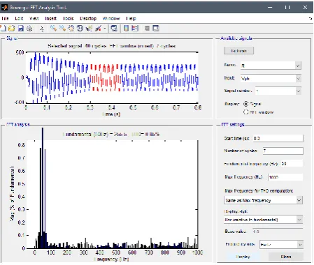
Fig.9: FFT Analysis of output phase voltage inSPWM
14
Fig.10: FFT Analysis of output phase voltage in THPWM modulation.
Fig.7& 8 shows the simulation results using both modulations. From the FFT analysis of output phase voltage shown in Fig.9& 10 it can be seen that in the case of SPWM modulation THD is 1.05% and in case of THPWM modulation it is 0.85% only.
4.
HARDWARE IMPLEMENTATION
[image:5.595.55.280.76.266.2]AND EXPERIMENTAL RESULTS
[image:5.595.58.286.437.566.2]Fig. 11 shows the experimental setup, while Fig.12 report the main waveforms recorded with the different modulation schemes.
Fig.11: The THPWM/SPWM three-phase SSI-inverter
.
a)
(b)
Fig. 12 the output waveform when using: (a) SPWM modulation, (b) THIPWM modulation. (15V/div. was used
with a 1/10X probe).
Regarding the hardware implementation, Three-phase split-source inverter is designed using Protues software and implemented to convert the 100V input DC voltage into three-phase 180V/50Hz. A prototype of the Three-three-phase inverter, which is controlled by STM32F103C8T6 MCU is implemented. The inverter consists of six IGBT transistors, which are working as switching devices, the switching frequency of the transistors is 18 KHz, and the result of output voltage is 184Vrms when using SPWM method and 181Vrms when the THPWM is used. The experimental results show satisfactory performance regarding the DC-to-DC boosting stage and DC-to-AC stage of the inverter with a reasonable THD in both modulation schemes. The resulting THD was 3.89% when using SPWM modulation, 2.67% when using THPWM.
5.
CONCLUSION
The SPWM modulation method was less satisfactory as it needs much larger inductance value and the total harmonic distortion (THD) was slightly bigger (3.89%) than the THD achieved using the THPWM which was 2.67%. In future another modulation scheme can be examined in order to eliminate the low-frequency component in the inductor current and the capacitor voltage.
6.
ACKNOWLEDGMENTS
It is a great pleasure to acknowledge all those who have assisted and supported me for successfully completing the paper. I express my deep sense of gratitude to Asst. Prof. Dr. Fadhil Al-Qrimli, for the valuable guidance as well as timely advice, his guidance, patience and encouragement which helped me a lot in completing the paper successfully.
7.
REFERENCES
[1] F. Z. Peng, “Z-source inverter,” Industry Applications, IEEE Transactions on, vol. 39, no. 2, pp. 504–510, Mar 2003.
[2] Y. Siwakoti, G. Town, P. C. Loh, and F. Blaabjerg, “Y-source inverter,” in Power Electronics for Distributed Generation Systems (PEDG), 2014 IEEE 5th International Symposium on, June 2014, pp. 1–6. [3] A. Abdelhakim, “Analysis and modulation of the
[image:5.595.56.277.602.752.2]15 stresses,” in Industrial Technology (ICIT), 2015 IEEE
International Conference on, March 2015, pp. 926–934. [4] Y. Siwakoti, F. Z. Peng, F. Blaabjerg, P. C. Loh, and G.
Town, “Impedance-source networks for electric power conversion part i: A topological review,” Power Electronics, IEEE Transactions on, vol. 30, no. 2, pp. 699–716, Feb 2015.
[5] Y. Siwakoti, F. Z. Peng, F. Blaabjerg, P. C. Loh, G. Town, and S. Yang, “Impedance-source networks for electric power conversion part ii: Review of control and modulation techniques,” Power Electronics, IEEE Transactions on, vol. 30, no. 4, pp. 1887–1906, April 2015.
[6] Ahmed Abdelhakim, Paolo Mattavelli, Giorgio Spiazzi, „Split-Source Inverter‟, IECON2015-Yokohama November 9-12, 2015.
[7] R. Caceres and I. Barbi, “A boost dc-ac converter: analysis, design, and experimentation,” Power Electronics, IEEE Transactions on, vol. 14, no. 1, pp. 134–141, Jan 1999.
[8] Fang Zheng Peng, Miaosen Shen, Zhaoming Qian, “Maximum Boost Control of the Z-Source Inverter”, IEEE Transactions on Power Electronics, VOL. 20, No. 4, July 2005.
[9] Ahmed Abdelhakim, Paolo Mattavelli, Giorgio Spiazzi, “Three-phase Split-Source Inverter (SSI): Analysis and Modulation”, IEEE Transactions on Power Electronics, DOI 10.1109/TPEL.2015.2513204.
[10] D.A. Grant and J. A. Houldsworth, “ PWM AC Motor Drive Employing Ultrasonic Carrier”, IEE Conf. PE-VSD, London, 1984, pp. 234-240.