Modified qHAADF method for atomic column-by-column compositional quantification of semiconductor heterostructures
Atif A. Khan*,1, M. Herrera1, J. Pizarro2, P. L. Galindo2, P. J. Carrington3, H. Fujita4,5, A. Krier4, S. I. Molina1
*
Corresponding author: e-mail: [email protected], Phone: +34 65 443 08 21, ORCID: 0000-0002-0322-5024
1
Department of Material Science, Metallurgical Chemistry and Inorganic Chemistry, IMEYMAT, University of Cádiz, 11510 Puerto Real, Spain.
2
Department of Computer Engineering, ESI, University of Cádiz, 11510 Puerto Real, Spain. 3
Department of Engineering, Lancaster University, Lancaster, LA1 4YW, UK. 4
Physics Department, Lancaster University, Lancaster, LA1 4YB, UK 5
Asahi Kasei Corporation, 2-1 Samejima, Fuji-city, Shizuoka 416-8501, Japan
Authors: M. Herrera; e-mail: [email protected], ORCID: 0000-0002-2325-5941
J. Pizarro; e-mail: [email protected], ORCID: 0000-0002-4295-6743
P.L. Galindo; e-mail: [email protected], ORCID: 0000-0003-0892-8113
P.J. Carrington; e-mail: [email protected], ORCID: 0000-0003-2107-5602
H. Fujita; e-mail: [email protected], ORCID: 0000-0001-5081-5417
A. Krier; e-mail: [email protected], ORCID: 0000-0003-4098-5206
S.I. Molina; e-mail: [email protected], ORCID: 0000-0002-5221-2852
Abstract
The qHAADF method allows the quantification of the composition at atomic column resolution in semiconductor materials by comparing the HAADF-STEM intensities between a region of interest to a region of the material of known composition. However, the application of this qHAADF approach requires both regions to be differentiable and included in the same micrograph at close proximity. This limits the application of this approach to certain materials and magnifications where this requirement is fulfilled. In this work, we extend the qHAADF method to analyses where the reference region is imaged in a separate micrograph. The validity of this modified method is proved by comparison to the original qHAADF approach using HAADF-STEM simulated images of the semiconductor heterostructure InSb/InAs. Additionally, the methods are applied successfully to experimental images both of a simple InSb/InAs interface and of a complex InSb/GaSb heterostructure, justifying the significance of the modified method over the original method.
Keywords: HAADF-STEM, Modified qHAADF, Atomic-column resolution, Quantitative composition analysis, Semiconductors.
Introduction
the incident electron beams in order to quantify ADF images [24,26,27]. Additionally, it has been shown that empirical incoherent parametric imaging can be combined with frozen lattice multislice simulations in order to evolve from a relative toward an absolute quantification of the composition of single atomic columns [28]. Although theses methodologies have been shown to provide reliable results, they either require time consuming multiple experimental analyses in terms of variable image acquisition parameters or require additional complex instrumentation or not compatible to material segregation associated compositional quantification. As a result, a direct and faster compositional quantification model of quantitative HAADF (qHAADF) [29] has been developed that compares experimental HAADF-STEM integrated intensities of the region of interest (ROI) with the intensity of a homogenous (reference) area to quantify the composition [30], using a single set of image acquisition parameters. For example, the compositional distribution of Sb has been quantified within GaAs capped GaSb nanostructures [22] and in GaAsSbN capped InAs quantum dots (QDs) [31] using this method. However, this program only works when the ROI and reference regions are at the same HAADF-STEM image. This basic requirement limits this method to function in low magnification in terms of multi-layered structures, where the ROI and the reference area (typically, substrate) could be positioned far away from each other. Moreover, in the compositional quantification of highly segregating materials like Sb [32], locating a homogenous region is rather complicated, restraining functionality to this method.
In this paper, a modified version of the qHAADF program is presented. This version compares the integrated intensities of a ROI area to a homogenous (reference) area present in two separate HAADF-STEM images in order to generate a compositional map on the ROI image. The InSb/InAs material is considered to exemplify the method. Primarily, the compositional outcomes of the modified method applied to simulated InSb/InAs images are compared to the existing qHAADF method using various image-pixel accumulation areas (integration areas), and to the real composition in the simulated models, proving its validity. Later, the compatibility of the modified method to the original method is demonstrated in terms of experimental HAADF-STEM InAs/InSbxAs1-x/InAs images. As the final demonstration, another experimental HAADF-STEM image of alternating InSb/GaSb structure is considered which can potentially be analyzed by the modified method due to the absence of a reference region close to the ROI.
Materials and Methods
The electron transparent specimens for the HAADF-STEM analysis associated to both samples were prepared by mechanical thinning and Precision Ion Polishing System (PIPS) associated Ar+ ion milling. All experimental high resolution HAADF-STEM images of the prepared specimens were obtained using a JEOL JEM ARM 200cF single aberration corrected (condenser aberration) microscope working at an operating voltage of 200 kV, while having imaging parameters of Cs= -611 nm, C5= 817.2 mm, HAADF detector inner angle= 90 mrad, objective aperture angle= 15.2 mrad and defocus= -1 Å.
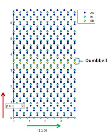
[image:4.595.182.369.364.598.2]Simulated HAADF images of InAs/InSb/InAs structures along [110] zone axis have been computed using the model illustrated in Fig. 1 where As columns are included as blue circles, In as cyan circles and Sb as yellow circles. In each simulated model, Sb columns are included within 3 central monolayers (MLs) as shown in Figure 1, with partial presence of As (InSbxAs1-x). Here, the nominal Sb composition (x) is varied from 0 to 0.5 with 0.1 increment. All the simulations were performed using SICSTEM software that runs on CAI supercomputer in UCA. The working principle of the SICSTEM software can be found here [33]. Aberration correction associated spatial incoherence was also considered during simulations [34].
Figure 1 Schematic of the model used for the simulation of the InAs/InSb/InAs layers. Results and discussion
Implementation of the method
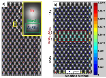
Figure 2 (a) HAADF-STEM simulated image of InSb0.5As0.5 where the group III (In) atomic columns are marked with red dots and the group V (As/Sb) atomic columns with blue dots. The inset represents a single dumbbell where a group V atomic column is surrounded by a Mask1 (green rectangle). (b) The modified qHAADF method generated 'R' map corresponds the image in a). The red rectangle represents the InSb0.5As0.5 area.
In order to assess the validity of the modified method, it has been compared to the original qHAADF method. For this, InAs dumbbells from the same image of InSb0.5As0.5 analyzed have been taken as the reference region for the calculation, and the same Mask 1 has been used while having the sample thickness of 20 nm. Our results have shown that the original method generates same 'R' values over same group V columns (not shown) as in Figure 2b. This outcome confirms that for a homogenous and same ROI-reference thickness, the modified method is compatible to the original method in terms of simulated images.
[image:6.595.112.486.103.377.2]Ri = 1 + a.xi (1)
where, xi represents As composition. They obtained the constant 'a' value by evaluating an As based statistical Ri vs. xi graph in terms of a few known xi compositions. They have also experimentally ensured that the effect of certain range of sample thicknesses over 'Ri' values is insignificant and hence, the variation in xi is the only effective contributing parameter here. Later on, the validity of the above mentioned equation was justified at [36] for other III-V ternary alloys. Here, the researchers proposed a direct approach to obtain the constant 'a' value by summing monolayer-by-monolayer average 'Ri' values within certain number of MLs (N), where the both analyzing and
reference materials must be present at the same HAADF-STEM image. Their proposed equation was
= N + a. (2)
This equation illustrates the total change in the Ri value due to total deposition of xi within certain number of MLs (N). This equation provides the 'a' value, which later can be used to obtain average monolayer-by-monolayer or column-by-column xi values.
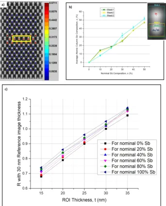
We have applied the methodology above for the quantification of Sb in our simulated HAADF images using the 'R' values obtained with the modified method shown in Figure 2b. Initially, 'a' has been obtained using total deposited xi values and corresponding average monolayer-by-monolayer Ri values within N MLs. For that, 17 MLs in the ROI image have been chosen (N = 17) as it ensures that the 3 Sb containing MLs are present within that 17 MLs while ignoring the simulation oriented boundary errors. Next, the obtained 'a' value is used in the first equation and Sb associated by-column local composition map is generated. Figure 3a represents the column-by-column local composition values calculated for the image corresponding to InSb0.5As0.5 through red dots. Here, to maintain simplicity evaluating the Mask1 associated deviation between the nominal (x = 0.5) and calculated values, four central group V columns have been chosen, represented within a yellow rectangle. The obtained average value of Sb composition associated to those four dumbbells has been found to be 47.38 % with a standard estimation error of 3.77%. This error falls within 99.9% of confidence level to the average value associated to statistical two-sided t-distribution, signifying that the composition of 47.38±3.77% assures 99.9% certainty to the true (nominal) value. In order to determine whether this method is also good for other nominal compositions, column-by-column Sb composition quantification maps have been generated for the Sb nominal values of 0.1≤x≤0.4 (not shown) with 0.1 increment. Figure 3b shows a graph of the average atomic column Sb composition (xi) vs. nominal Sb composition associated to Mask1 for images with 0≤x≤0.5 (in green). Here, the Mask1 based overall standard error obtained from the calculated profile (Mask1) is found to be only 4.37%, assuring that the modified qHAADF method is in a good agreement with the expected values in terms of all nominal compositions of 0≤x≤0.5.
would be more appropriate for composition quantification. For example, Mask1 functions appropriately in terms of very thin samples, ranging from 15-40 nm [34] since the investigating atomic column stays unaffected by the surrounding dumbbells in this thickness range [29]. On the other hand, some researchers suggested a Mask that contains the whole analyzing atomic column proving to provide better HAADF quantitative approach in terms of varying convergence angle, magnification, source size and defocus [38], sample associated small mis-tilt [39], aberrations and astigmatism [40] and scan induced noises [41], as long as the probe size does not change with the sample thickness. These characteristics allow possibility analyzing even thicker samples than of Mask1. In addition, another Mask has been suggested that imposes rectangular Voronoi cell [42] around each whole dumbbell that allows analyzing even thicker samples by providing an average value closer to the nominal [37]. Moreover, for a HAADF-STEM detection angle of 90 mrad, these Voronoi cells are sensitive to sample thickness induced effect [25] and hence, compositional quantification with a higher precision is expected as the thickness contribution to the HAADF-STEM signal can be identified. Because of these arguments, along with Mask1, the modified qHAADF program has been examined with two other Mask sizes, termed as Mask2 (covers each whole group V column) and Mask3 (covers each whole dumbbell) in terms of simulated images, while both ROI and reference images possess same specimen thickness of 20 nm. Figure 3b shows Mask1 (green), Mask2 (yellow) and Mask3 (cyan) originated graphs in terms of the average atomic column Sb compositions (xi), associated to the same dumbbells within the yellow rectangle as in Figure 3a vs. varying nominal Sb composition (0≤x≤0.5). For clarity, Figure 3b includes an inset showing a single In-As/Sb dumbbell where the three masks considered have been graphically represented. Here, the Mask1 based overall standard error obtained from the calculated profile (Mask1) is found to be only 4.37%. Again, the overall standard errors corresponding to Mask2 and Mask3 have also been found to be very small as 3.96% and 2.63%, respectively. Thus, our results show that in terms of simulated HAADF-STEM images with same specimen thickness, the three mask sizes considered are appropriate for the composition quantification. The high level of accuracy obtained could face slight degradation in terms of experimental analysis if the required parameters are not calibrated properly during the image acquisition. For example, to obtain the 'R' values, it is essential that both the ROI and reference HAADF-STEM images possess same image contrast, brightness and magnification. Once the necessary calibrations are performed, this modified method will offer benefits analyzing high resolution HAADF-STEM images associated to very high magnifications, since the ROI and reference regions do not need to be present in the same image. For example, the high resolution compositional quantification of a highly segregating material such as Sb [32] within a complex micro structure can be performed using this method without finding a pure homogenous area in the same HAADF-STEM image.
of this, in the present paper we address the issue of errors due to the specimen thickness considering the case where the ROI and the reference images correspond to regions of the specimen with different thicknesses. For this, we have measured the R values for InSbxAs1-x (ROI) images with thickness 15 nm to 35 nm considering reference InAs regions with average thickness of 30 nm, for Sb compositions of 0% to 100%, and we show the results obtained in Figure 3.c. As observed in this Figure, for each 1 nm increment at the specimen thickness, the R values increase by a factor of ~ 0.02 ± 0.004 for every Sb composition. For this thickness range, equation (1) can be re-written as
R = 1 + a.xi ± 0.02.Δt (3)
Figure 3 (a) Atomic column composition map calculated from the modified qHAADF originated 'R' values shown in Figure 2b, superimposed to the HAADF-STEM simulated image. (b) Graph of the average atomic column Sb composition calculated from the modified qHAADF originated 'R' values vs. the nominal Sb composition for the three masks considered. The error bars illustrates standard deviations to the corresponding averages. The inset represents the three mask areas considered: Mask1 (green), Mask2 (yellow) and Mask3 (cyan), surrounding a single In-As/Sb dumbbell. (c) Plots of Sb composition induced R vs specimen thickness effect as per simulated HAADF-STEM signals with ROI thicknesses of 15-35 nm in association to average reference thickness of 30 nm.
[image:10.595.145.488.104.530.2]for quantitative purposes, image simulations need to be taken into account to recalculate the obtained values considering the thickness variations measured in order to obtain precise composition values. In order to do that, in this case equation (3) above can be used. For values of Δt of 1nm and R ~ 1.06, we obtain a x value of ~ 26%, which is very close to the value obtained with the original method, as expected.
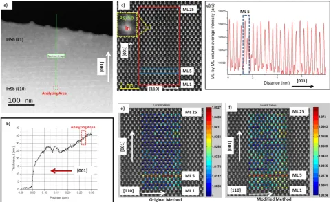
Figure 4 (a) Low-mag HAADF-STEM image where the red rectangle depicts the location of the analyzing ROI and Reference areas; (b) corresponding thickness profile associated to the Spectrum image line (green line), along with the analyzing area in Fig. 4a. (c) Experimental HAADF-STEM image of InSb/InAs (single In-As/Sb dumbbell at the inset); (d) intensity profile obtained from the image in Fig. 4c, evidencing the position of the InSb layer; R map calculated with the original (e) and modified (f) methods, from the HAADF-STEM image in Fig. 4c.
[image:12.595.56.538.194.488.2]Figure 5 (a) HAADF-STEM image of InSb/GaSb (ROI area) and (b) the corresponding absolute thickness profile; (c) HAADF-STEM image of the GaSb buffer layer (reference area) and (d) the corresponding thickness profile taken from the region on the white rectangle at Fig. 5c; (e) R map on the ~ 4 nm ROI area within the selected thickness range in Fig. 5b, calculated with the modified method; (f) Plots of In composition induced R vs specimen thickness effect as per simulated HAADF-STEM signals with ROI thicknesses of 21-27 nm in association to average Reference thickness of 21 nm.
Conclusions
We have developed a modified qHAADF method for the quantitative analysis of the composition with atomic column resolution for cases where the ROI and the reference regions are imaged in separate HAADF-STEM micrographs. The compatibility of this method to the original method has been justified with the help of simulated HAADF-STEM images of InAs/InSbxAs1-x/InAs, where 0≤x≤0.5. The compatibility between the methods in terms of experimental InSb/InAs structures HAADF-STEM images has also been proved. Additionally, the significance of the modified method over the original method is justified in terms of HAADF-STEM compositional analysis of InSb/GaSb structure, situated far away from the homogeneous GaSb buffer layer.
Acknowledgements
This work was supported by European Union (UE) (post graduate research on dilute metamorphic nanostructures and metamaterials in semiconductor photonics (PROMIS) Horizon 2020 initial training network (ITN) project), Spanish MINECO (projects TEC2014-53727-C2-2-R and TEC2017-86102-C2-2-R) and the Junta de Andalucía (PAI research groups TEP-946 INNANOMAT and TIC-145). Co-financing from UE-FEDER is also acknowledged.
Conflict of interest
The authors declare that they do not have any conflict of interest. References
[1] Pennycook SJ, Rafferty B and Nellist PD (2000) Z-contrast imaging in an aberration-corrected scanning transmission electron microscope, Microsc.& Microanal.6:343-352.
[2] Pennycook SJ and Boatner LA (1988) Chemically sensitive structure-imaging with a scanning electron microscope, Nature 336:565-567.
[3] Batson PE, Dellby N and Krivanek OL (2002) Sub-ångstrom resolution using aberration corrected electron optics, Nature 418:617-620.
[4] Muller DA, Nakagawa N, Ohtomo A, Grazul JA and Hwang HY (2004) Atomic-scale imaging of nanoengineered oxygen vacancy profiles in SrTiO3, Nature 430:657-661.
[6] Kaiser U, Muller DA, Grazul JL, Chuvilin A and Kowasaki M (2002) Direct observation of defect-mediated cluster nucleation, Nat. Mat. 1:102-105.
[7] Yamazaki T, Nakanishi N, Recnik A, Kawasaki M, Watanabe K, Ceh M and Shiojiri M (2004) Quantitative high-resolution HAADF-STEM analysis of inversion boundaries in Sb2O3-doped zinc oxide, Ultramic. 98:305-316.
[8] Anderson SC, Birkeland CR, Anstis GR and Cockayne DJH (1997) An approach to quantitative compositional profiling at near-atomic resolution using high-angle annular dark field imaging, Ultramic. 69:83-103.
[9] Klie RF and Zhu Y (2005) Atomic resolution STEM analysis of defects and interfaces in ceramic materials, Micron 36:219-231.
[10] Klenov DO and Stemmer S (2006) Contributions to the contrast in experimental high-angle annular dark-field images, Ultramic. 106:889-901.
[11] Wang P, Bleloch AL, Falke M, Goodhew PJ, Ng J and Missous M (2006) Direct measurement of composition of buried quantum dots using aberration-corrected scanning transmission electron microscopy, Appl. Phys. Lett. 89:072111.
[12] Mokkapati S and Jagadish C (2009) Review: III-V compound SC for optoelectronic devices, Mater. Today 12:22-32.
[13] Semenov A, Lyublinskaya OG, Solov’ev VA, Meltser BY and Ivanov SV (2007) Surface segregation of Sb atoms during molecular-beam epitaxy of InSb quantum dots in an InAs(Sb) matrix, J. Cryst. Growth 301-302:58-61.
[14] Namazi L, Ghalamestani SG, Lehmann S, Zamani RR and Dick KA (2017) Direct nucleation, morphology and compositional tuning of InAs1-xSbx nanowires on InAs (111) B substrates, Nanotech. 28:165601.
[15] Zhang Y, Wu J, Aagesen M and Liu H (2015) Review: III-V nanowires and nanowire optoelectronic devices, J. Phys. D: Appl. Phys. 48:463001.
[16] Bonef B, Gérard L, Rouvière JL, Grenier A, Jouneau PH, Bellet-Amalric E, Mariette H, André R and Bougerol C (2015) Atomic arrangement at ZnTe/CdSe interfaces determined by high resolution scanning transmission electron microscopy and atom probe tomography, Appl. Phys. Lett. 106:051904.
[17] Tey CM, Liu HY, Cullis AG, Ross IM and Hopkinson M (2005) Structural studies of a combined InAlAs-InGaAs capping layer on 1.3-µm InAs/GaAs quantum dots, J. Cryst. Growth 285:17-23.
[18] Chery N, Ngo TH, Chauvat MP, Damilano B, Courville A, Mierry PD, Grieb T, Mehrtens T, Krause FF, Caspary KM, Schowalters M, Gil B, Rosenauer A and Ruterana P (2017) The microstructure, local indium composition and photoluminescence in green-emitting InGaN/GaN quantum wells, J. Mic. 00:1-8.
[19] Groiss H, Spindlberger L, Oberhumer P, Schäffler F, Fromherz T, Grydlik M and Brehm M (2017) Photoluminescence enhancement through vertical stacking of defect-engineered Ge on Si quantum dots, Semicond. Sci. Technol. 32:02LT01.
[20] Nie JF (2017) IOP Conf. Series: Mat. Sci. Eng. 219:012005.
[22] Molina SI, Beltrán AM, Ben T, Galindo PL, Guerrero E, Taboada AG, Ripalda JM and Chisholm MF (2009) High resolution electron microscopy of GaAs capped GaSb nanostructures, Appl. Phys. Lett. 94:043114.
[23] Broek WVD, Rosenauer A, Goris B, Martinez GT, Bals S, Aert SV and Dyck DV (2012) Correction of non-linear thickness in HAADF-STEM electron tomography, Ultamic. 116:8-12. [24] Rosenauer A, Gries K, Müller K, Pretorius A, Schowalter M, Avramescu A, Engl K and
Lutgen S (2009) Measurement of specimen thickness and composition in AlxGa1-xN/GaN using high-angle annular dark field images, Ultramic. 109:1171-1182.
[25] Caspary KM, Oppermann O, Grieb T, Krause FF, Rosenauer A, Schowalter M, Mehrtens T, Beyer A, Volz K and Potapov P (2016) Material characterization by angle-resolved scanning transmission electron microscopy, Sci. Rep. 6:37146.
[26] LeBeau JM, Findlay SD, Allen LJ and Stemmer S (2008) Quantitative atomic resolution scanning transmission electron microscopy, Phys. Rev. Lett. 100:206101.
[27] LeBeau JM, Findlay SD, Wang X, Jacobson AJ, Allen LJ and Stemmer S (2009) High-angle scattering of fast electrons from crystals containing heavy elements: simulation and experiment, Phys. Rev. B 79:214110.
[28] Martinez GT, Rosenauer A, Backer AD, Verbeeck J and Aert SV (2014) Quantitative composition determination at the atomic level using model-based high-angle annular dark field scanning transmission electron microscopy, Ultramic. 137:12-19.
[29] Molina SI, Sales DL, Galindo PL, Fuster D, González Y, Alén B, González L, Varela M and Pennycook SJ (2009) Column-by-column compositional mapping by Z-contrast imaging, Ultramic. 109:172-176.
[30] Molina SI, Galindo PL, Gonzalez L, Ripalda JM, Varela M and Pennycook SJ (2010) Exploring semiconductor quantum dots and wires by high resolution electron microscopy, J. Phys.: Conf. Series 209:012004.
[31] Reyes DF, González D, Ulloa JM, Sales DL, Dominguez L, Mayoral A and Hierro A (2012) Impact of N on the atomic-scale Sb distribution in quaternary GaAsSbN-capped InAs quantum dots, Nanosc. Res. Lett. 7:653.
[32] Lu J, Luna E, Aoki T, Steenbergen EH, Zhang YH and Smith DJ (2016) Evaluation of Sb segregation in InAs/InAs1-xSbx type-II superlattices grown by molecular beam epitaxy, Appl. Phys. Lett. 119:095702.
[33] Pizarro J, Galindo PL, Guerrero E, Yáñez A, Guerrero MP, Rosenauer A, Sales DL, Molina SI (2008) Simulation of high angle annular dark field scanning transmission electron microscopy images of large nanostructures, App. Phys. Lett. 93:153107.
[34] Molina SI, Guerrero MP, Galindo PL, Sales DL, Varela M and Pennycook SJ (2011) Calculation of integrated intensities in aberration-corrected Z-contrast images, J. Elect. Microsc. 60:29-33.
[35] Galindo PL, Kret S, Sanchez AM, Laval JY, Yáñez A, Pizarro J, Guerrero E, Ben T, Molina SI (2007) The Peak Pairs algorithm for strain mapping from HRTEM images, Ultramic. 107:1186-1193.
[37] Jones L (2016) Quantitative ADF-STEM: acquisition, analysis and interpretation, IOP Conf. Series: Mat. Sci. Engg. 109:012008.
[38] MacArthur HE, MacArthur KE, Pennycook TJ, Okunishi E, D’Alfonso AJ, Lugg NR, Allen LJ and Nellist PD (2013) Probe integrated scattering cross sections in the analysis of atomic resolution HAADF STEM images, Ultramic. 133:109-119.
[39] MacArthur KE, D’Alfonso AJ, Ozkaya D, Allen LJ and Nellist PD (2015) Optimal ADF STEM imaging parameters for tilt-robust image quantification, Ultramic. 156:1-8.
[40] Martinez GT, Backer AD, Rosenauer A, Verbeeck J and Aert SV (2013) The effect of probe inaccuracies on the quantitative model-based analysis of high angle annular dark field scanning transmission electron microscopy images , Micron 63:57-63.
[41] Jones L and Nellist PD (2013) Identifying and correcting scan noise and drift in the scanning transmission electron microscope, Microsc. & Microanal.19:1050-1060.
[42] Aurenhammer F (1991) Voronoi diagrams - A survey of fundamental geometric data structure, ACM Comp. Surv. 23:345-405.
[43] Malis T, Cheng SC and Egerton RF (1988) EELS log-ratio technique for specimen-thickness measurement in the TEM, J. Elect. Micro. Tech. 8:193-200.
[44] Wiener N (1949) Extrapolation, Interpolation and Smoothing of stationary time series. Wiley, New York.
[45] Haxha V, Drouzas I, Ulloa JM, Bozkurt M, Koenraad PM, Mowbray DJ, Liu HY, Steer MJ, Hopkinson M and Migliorato MA (2009) Role of segregation in InAs/GaAs quantum dot structures capped with a GaAsSb strain-reduction layer, Phys. Rev. B 80:165334.