ENGINEERING COMMITTEE
Interface Practice Subcommittee
AMERICAN NATIONAL STANDARD
ANSI/SCTE 46 2014
NOTICE
The Society of Cable Telecommunications Engineers (SCTE) Standards and Recommended Practices (hereafter called documents) are intended to serve the public interest by providing specifications, test methods and procedures that promote uniformity of product, interchangeability, best practices and ultimately the long term reliability of broadband communications facilities. These documents shall not in any way preclude any member or non-member of SCTE from manufacturing or selling products not conforming to such documents, nor shall the existence of such standards preclude their voluntary use by those other than SCTE members, whether used domestically or internationally.
SCTE assumes no obligations or liability whatsoever to any party who may adopt the documents. Such adopting party assumes all risks associated with adoption of these documents, and accepts full responsibility for any damage and/or claims arising from the adoption of such Standards. Attention is called to the possibility that implementation of this document may require the use of subject matter covered by patent rights. By publication of this document, no position is taken with respect to the existence or validity of any patent rights in connection therewith. SCTE shall not be responsible for identifying patents for which a license may be required or for conducting inquiries into the legal validity or scope of those patents that are brought to its attention.
Patent holders who believe that they hold patents which are essential to the implementation of this document have been requested to provide information about those patents and any related licensing terms and conditions. Any such declarations made before or after publication of this document are available on the SCTE web site at http://www.scte.org.
All Rights Reserved
© Society of Cable Telecommunications Engineers, Inc. 140 Philips Road
TABLE OF CONTENTS 1.0 SCOPE ...1 2.0 NORMATIVE REFERENCES ...1 3.0 COMPLIANCE NOTATION ...1 4.0 DEFINITIONS ...2 5.0 EQUIPMENT ...4 6.0 SET-UP ...4 7.0 TEST PROCEDURES ...6 LIST OF FIGURES
FIGURE 1 – POWER TRIANGLE 2
FIGURE 2 – CONNECTION DIAGRAM 5
FIGURE 3 – PROBE CONNECTION EXAMPLE 10
FIGURE 4 – HOLD-UP TIME 11
FIGURE 5 – IN-RUSH CURRENT 13
FIGURE 6 – START-UP TIME 15
LIST OF TABLES
TABLE 1 – TEST EQUIPMENT 4
TABLE 2 – HOLD-UP TIME TEST – OSCILLOSCOPE CONFIGURATION 10 TABLE 3 – IN-RUSH CURRENT TEST – OSCILLOSCOPE CONFIGURATION 12 TABLE 4 – START-UP TIME TEST – OSCILLOSCOPE CONFIGURATION 14
1.0 SCOPE
The purpose of this standard is to characterize, document and define test methods for AC to DC outdoor plant power supplies. These tests involve the measurement of AC input parameters and DC output parameters. The application of uniform test methods for power supplies will allow fair performance comparisons to be made between different power supplies.
There are repetitive tests throughout this test document, in which many of the tests can be combined and performed at the same time.
2.0 NORMATIVE REFERENCES
The following documents contain provisions, which, through reference in this text, constitute provisions of the standard. At the time of Subcommittee approval, the editions indicated were valid. All standards are subject to revision; and while parties to any
agreement based on this standard are encouraged to investigate the possibility of applying the most recent editions of the documents listed below, they are reminded that newer editions of those documents may not be compatible with the referenced version. 2.1 SCTE References
ANSI/SCTE 96 2008 – Cable Telecommunications Testing Guidelines
ANSI/SCTE 82 2012 – Test Method for Low Frequency and Spurious Disturbances
3.0 COMPLIANCE NOTATION
“SHALL” This word or the adjective “REQUIRED” means that the item is an absolute requirement of this specification.
“SHALL NOT” This phrase means that the item is an absolute prohibition of this specification.
“SHOULD” This word or the adjective “RECOMMENDED” means that there may exist valid reasons in particular circumstances to ignore this item, but the full implications should be understood and the case carefully weighted before choosing a different course.
“SHOULD NOT”
This phrase means that there may exist valid reasons in particular circumstances when the listed behavior is acceptable or even useful, but the full implications should be understood and the case carefully weighed before implementing any behavior described with this label.
“MAY” This word or the adjective “OPTIONAL” means that this item is truly optional. One vendor may choose to include the item because a particular marketplace requires it or because it enhances the product, for example; another vendor may omit the same item.
4.0 DEFINITIONS
4.1 Power Consumption
4.1.1 Apparent AC Power: the scalar product of the RMS input voltage and RMS input current (Eq. 1)
(Eq.1) PIN(app)=VIN×IIN (VA)
The apparent power unit is volt-ampere (VA) and is the vector sum of the real and reactive power vectors in the power triangle (Figure 1)
Figure 1 – Power Triangle
4.1.2 Real AC Power: the instantaneous product of the time varying voltage and time varying current (Eq. 2)
(Eq. 2) =
∫
T ⋅ 0 IN v (t) i (t)dt T 1 (real) P IN IN (watts)where T is the period of the waveform
4.2 Efficiency: the ratio of output power to input power. This unit-less parameter will be expressed in percentage form. Efficiency is calculated using (Eq. 3)
(Eq. 3)
where POUT= VOUT × IOUT and ‘n’ represents the number of outputs
Real Power Reactive Power Apparent Power × =
∑
= (real) p p 100 %Eff IN n 1 m m OUT4.3 AC Input Loading: the relationship of a change in the input current usage versus a change in the input voltage for a constant load on the output. This is a directly measured set of data.
4.4 Line Regulation: the relationship of a change in the output DC voltage versus a change in the AC input voltage while holding the load current constant. This may be expressed as a difference between two input conditions.
(Eq. 4) Lineregulation (mV)= (VOUT)INPUTSTATE 1 −(VOUT)INPUTSTATE 2 4.5 Load Regulation: the relationship of a change in the output DC voltage versus a
change in the DC output load current while holding the input voltage constant. This may be expressed as a difference between the rated load state and the specified minimum load state.
(Eq. 5) Loadregulation (mV)= (VOUT)LOADSTATE1−(VOUT)LOADSTATE2
4.6 Power Factor: the ratio of the real power to the apparent power required to operate a device (see Figure 1). Power Factor may be measured directly (from a power
analyzer) or it may be calculated using the following relationship (refer to Eq. 1 and Eq. 2)
(Eq. 6)
4.7 Voltage Ripple: the amplitude of any residual AC voltage which is present on the DC output of the DUT. The “voltage ripple” is a directly measured quantity.
4.8 DUT: the “device under test” for this test procedure refers to the DC power supply assembly only. It may be tested within the confines of the "intended device" (for heat distribution and filtering purposes), but the input and output connections must be separated from the “intended device” to allow greater control of test conditions. Final performance within the “intended device” should reflect equivalent performance. 4.9 Hold-up Time: the time duration from when the AC input voltage is removed from
the power supply input until the output voltage falls below the minimum
specification. The AC input voltage shall be removed at the zero crossing (within ±1 msec of the zero crossing) of the input waveform.
4.10 In-rush Current: the instantaneous peak input current that is measured during the initial powering sequence. It shall be performed with the AC input voltage at or near
(app) P (real) P PF IN IN =
the zero crossing (within ±1 msec of the zero crossing). It is to be performed with the power supply capacitors completely discharged (>99% discharged).
4.11 Start-up Time: the time duration from the first in-rush current pulse to the time when all DC output voltages reach their minimum specified operating points. Note that the in-rush current timing reference is the same as in 4.10 (above).
5.0 EQUIPMENT
5.1 The Test Procedure Introduction document, ANSI/SCTE 96 2008, describes and specifies some of the basic test equipment which may be required. Much of the equipment required for these procedures is more specialized in nature. Details as to specific requirements will be called out within the individual test procedures, as needed.
5.2 Table 1 is a list of suitable test equipment. Functionally equivalent units may be substituted as desired.
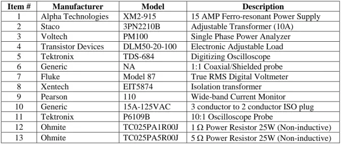
Table 1 – Test Equipment
Item # Manufacturer Model Description
1 Alpha Technologies XM2-915 15 AMP Ferro-resonant Power Supply 2 Staco 3PN2210B Adjustable Transformer (10A)
3 Voltech PM100 Single Phase Power Analyzer 4 Transistor Devices DLM50-20-100 Electronic Adjustable Load 5 Tektronix TDS-684 Digitizing Oscilloscope 6 Generic NA 1:1 Coaxial/Shielded probe 7 Fluke Model 87 True RMS Digital Voltmeter 8 Xentech EIT5874 Isolation transformer
9 Pearson 110 Wide-band Current Monitor
10 Generic 15A-125VAC 3 conductor to 2 conductor ISO plug 11 Tektronix P6109B 10:1 Oscilloscope Probe
12 Ohmite TC025PA1R00J 1 Ω Power Resistor 25W (Non-inductive) 13 Ohmite TC025PA5R00J 5 Ω Power Resistor 25W (Non-inductive)
6.0 SET-UP
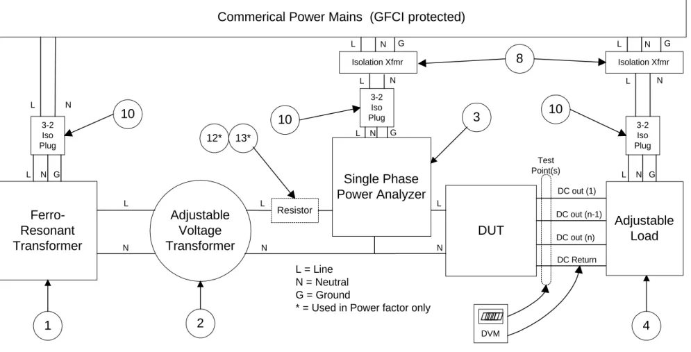
6.1 Construct the test system as shown in Figure 2. Note the use of “isolation” plugs isolates the ground return; therefore the devices should be powered from a ground fault circuit interrupting system (GFCI).
6.2 All wiring should be of a sufficient gauge to minimize voltage drops due to wire resistance.
Note: Extreme care should be exercised whenever exposed AC wiring and hazardous voltages and high temperatures are present
Figure 2 – Connection Diagram
Ferro-Resonant Transformer Adjustable Voltage Transformer
Commerical Power Mains (GFCI protected)
DUT Single Phase Power Analyzer 3-2 Iso Plug 3-2 Iso Plug 3-2 Iso Plug 1 2 3 4 L N G L N G L N G L N L N L N DC out (1) DC out (n) DC out (n-1) 10 10 10 DC Return L = Line N = Neutral G = Ground
* = Used in Power factor only
Resistor 13* L N 12* L N Isolation Xfmr L N G L N Isolation Xfmr L N G 8 DVM Adjustable Load Test Point(s)
7.0 TEST PROCEDURES
The power supply unit (DUT) will be tested as a stand-alone unit electrically independent of the intended equipment. It may be tested within the confines of the "intended device" (for heat distribution and filtering purposes), but the input and output connections must be separated from the “intended device” to allow greater control of test conditions. Final performance within the “intended device” should reflect equivalent performance. To evaluate noise and other spurious emissions, testing should be performed within the intended equipment by referring to ANSI/SCTE 82 2012.
7.1 Power Consumption
7.1.1 Set the input AC voltage to the maximum specified input level using the adjustable transformer (Figure 2 Item #2). Measure the input voltage using the power analyzer (Figure 2 Item #3).
7.1.2 Set the electronic load (Figure 2 Item #4) to the specified maximum output load current. Use a DVM (Figure 2 Item #7) in series with the DC output or the electronic load ammeter (Figure 2 Item #4) may also be used. If the power supply being tested has multiple DC voltage outputs adjust each DC output to the specified maximum output load current. Readjust the input AC voltage if it has changed.
7.1.3 Using the power analyzer, measure and record the input AC power consumption, PIN(real), and the input AC voltage, VIN (Figure 2 Item #3). 7.1.4 Holding the input AC voltage constant, adjust the electronic load(s) on the DC
output(s) to the next load current(s) as desired. Readjust the input AC voltage (Figure 2 Item #2) if it has changed. Repeat the measurements of 7.1.3 for each current.
7.1.5 Repeat 7.1.2 through 7.1.4 while adjusting the input AC voltage transformer in steps, as desired, from the maximum to the minimum rated input levels for the AC voltage.
7.2 AC Input Loading
7.2.1 Set the input AC voltage to the maximum specified input level using the adjustable transformer. Measure the input voltage using the power analyzer (Figure 2 Item #3).
7.2.2 Adjust the electronic load (Figure 2 Item #4) to the specified maximum output load current. Use a DVM (Figure 2 Item #7) in series with the DC output or the electronic load ammeter may also be used. If the power supply being tested has multiple DC voltage outputs adjust each DC output to the specified maximum output load current. Readjust the input AC voltage if it changed.
7.2.3 Using the power analyzer (Figure 2 Item #3), measure and record the input AC current, IIN, versus the input AC voltage, VIN.
7.2.4 Holding the input AC voltage constant, adjust the electronic load(s) on the DC output(s) to the next load current(s) as desired. Readjust the input AC voltage (Figure 2 Item #2) if it has changed. Repeat the measurements of 7.2.3 for each current.
7.2.5 Repeat 7.2.2 through 7.2.4 while adjusting the input AC voltage transformer in steps, as desired, from the maximum to the minimum rated input levels for the AC voltage.
7.3 Efficiency
7.3.1 Set the input AC voltage to the maximum specified input level using the adjustable transformer. Measure the input voltage using the power analyzer (Figure 2 Item #3).
7.3.2 Adjust the electronic load (Figure 2 Item #4) to the specified maximum output load current. If the power supply being tested has multiple DC voltage outputs adjust each DC output to the specified maximum output load current. Readjust the input AC voltage if it changed.
7.3.3 Using the power analyzer (Figure 2 Item #3), measure and record the input AC “real power,” PIN(real).
7.3.4 Calculate the power of the DC output(s) using the following equation: (Eq. 7)
7.3.5 Calculate and record the efficiency using Eq. 3.
7.3.6 Holding the input AC voltage constant, adjust the electronic load(s) on the DC output(s) to the next load current(s) as desired. Readjust the input AC voltage if it changed. Repeat the measurements of 7.3.3 through 7.3.5 for each current. 7.3.7 Repeat 7.3.2 through 7.3.6 while adjusting the input AC voltage transformer in
steps, as desired, from the maximum to the minimum rated input levels for the AC voltage.
7.4 Load Regulation
7.4.1 Connect the DC voltmeter to the output of the power supply when making a DC voltage measurement.
∑
∑
= =×
=
=
n 1 m OUT OUT n 1 m OUT TOTALP
(V
I
)
P
m m m7.4.2 Using the power analyzer (Figure 2 Item #3), set the input AC voltage to the maximum specified input level using the adjustable transformer (Figure 2 Item #2).
7.4.3 Adjust the electronic load (Figure 2 Item #4) to the specified maximum output load current. If the power supply being tested has multiple DC voltage outputs adjust each DC output to the specified maximum output load current. Readjust the input AC voltage if it changed.
7.4.4 Using the DC voltmeter (Figure 2 Item #7), measure and record the DC voltage, VOUT.
7.4.5 Adjust the electronic load(s) on the DC output(s) to the next desired value of current load. Readjust the input AC voltage if it changed. Using the DC
voltmeter (Figure 2 Item #7), measure and record the DC voltage. Calculate and record the load regulation from Eq. 5.
7.4.6 Repeat 7.4.5 for each desired load current using uniform steps, as desired, from the maximum to the minimum rated levels for each output current.
7.5 Line Regulation
7.5.1 Connect the DC voltmeter to the output of the power supply when making a DC voltage measurement (Figure 2 Item #7).
7.5.2 Using the power analyzer (Figure 2 Item #3), set the input AC voltage to the maximum specified input level using the adjustable transformer (Figure 2 Item #2).
7.5.3 Adjust the electronic load (Figure 2 Item #4) to the specified maximum output load current. If the power supply being tested has multiple DC voltage outputs adjust each DC output to the specified maximum output load current. Readjust the input AC voltage if it changed.
7.5.4 Using the DC voltmeter (Figure 2 Item #7), measure and record the DC voltage, VOUT.
7.5.5 Adjust the AC input voltage using the adjustable transformer (Figure 2 Item #2) to the next desired value. Using the DC voltmeter (Figure 2 Item #7), measure and record the DC voltage for each input setting. Calculate and record the line regulation from Equation 4.
7.5.6 Repeat 7.5.5 for the entire AC input voltage range using uniform steps, as desired, from the maximum to the minimum rated levels for input AC voltage.
7.6 Noise and Ripple
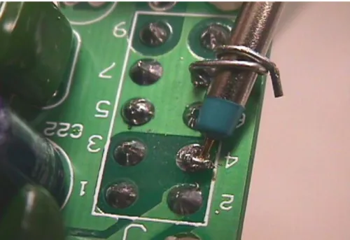
7.6.1 Connect an oscilloscope (Figure 2 Item #5) to the output of the power supply with a 1:1 probe (Figure 2 Item #6). The probe should consist of a short section of shielded coaxial cable.
7.6.2 For best results, minimize the distance from the power supply printed wiring board (PWB) to the probe on both the DC out and the ground connections. Shorter lead lengths lower the potential for picking up extraneous noise during the measurement.
7.6.3 If the final stages of power supply filtering are external to the DUT, it is
permissible to include the filtering circuitry in this test. This should be done by placing the DUT and the filtering circuitry in their "intended device." The connections between the filtering circuitry and the "intended device" must be broken to allow connection of the DUT output to the electronic load. The scope probe should be connected as close as possible to the output of the filtering circuitry.
7.6.4 If possible, remove the alligator clip ground from the probe and take a very small jumper from the ground of the PWB to the ground sheath of the probe (refer to Figure 3).
7.6.5 Using the power analyzer (Figure 2 Item #3), set the input AC voltage (Figure 2 Item #2) to the maximum specified input level using the adjustable transformer. 7.6.6 Adjust the electronic load (Figure 2 Item #4) to the specified maximum output
load current. If the power supply being tested has multiple DC voltage outputs adjust each DC output to the specified maximum output load current. Readjust the input AC voltage if it changed.
7.6.7 Using the oscilloscope (Figure 2 Item #5) with the 20 MHz bandwidth limit filter enabled, measure and record the peak-to-peak amplitude of the DC output voltage ripple and switching noise (Note that when using a digital sampling oscilloscope to measure noise and transient type signals, that some form of peak-detection sampling should be used).
7.6.8 The noise and ripple amplitude is the highest peak-to-peak combination of the power line frequency (and harmonically related) ripple and the other high frequency noise. Record the noise and ripple amplitude.
7.6.9 Holding the input AC voltage constant, adjust the electronic load(s) on the DC output(s) to the next load current(s) as desired. Readjust the input AC voltage if it changed. Repeat the measurements of 7.6.7 through 7.6.8 for each current. 7.6.10 Repeat 7.6.6 through 7.6.9 while adjusting the input AC voltage transformer in
steps, as desired, from the maximum to the minimum rated input levels for the AC voltage.
Figure 3 – Probe Connection Example
7.7 Hold-up Time
7.7.1 Using a dual channel digitizing storage oscilloscope (Figure 2 Item #5), probe the DC output on channel 1 and the AC input on channel 2. If the DUT has more than one output, all outputs should be tested and characterized. Set up the oscilloscope as outlined below:
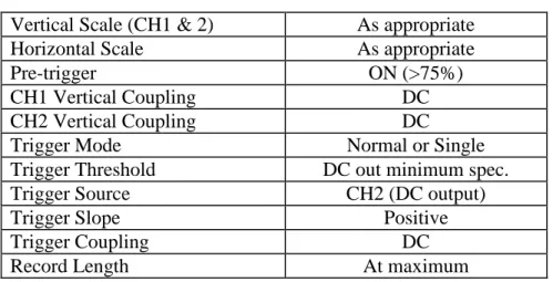
Table 2 – Hold-up Time Test – Oscilloscope Configuration
Vertical Scale As appropriate
Horizontal Scale As appropriate
Pre-trigger ON
CH1 Vertical Coupling DC
CH2 Vertical Coupling AC
Trigger Mode Normal or Single
Trigger Threshold 10% below DC out minimum spec.
Trigger Source CH1 (DC output)
Trigger Slope Negative
Trigger Coupling DC
7.7.2 Verify that the DUT is operating and set the load at the output(s) using the electronic load(s) to the specified maximum output load current. Note that in this test, all output(s) must be properly loaded although only one output is measured at a time. Set the AC power source to the minimum specified operating voltage.
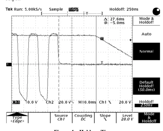
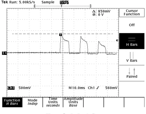
7.7.3 Find out where you are within the cycle, to make sure you have zero crossing correct to within ±1 milliseconds. Turn the AC source off. The oscilloscope should have triggered as the output voltage decreased below the trigger
threshold. The oscilloscope should display the AC and DC waveforms similar to the sample plot in Figure 4.
7.7.4 The holdup time is the time duration of when the AC input voltage is removed to the time until the output voltage falls below the minimum specification. The AC input voltage shall be removed within ±1 milliseconds of the zero crossing. This is shown in Figure 4 by the two vertical cursors. Record the holdup time. 7.7.5 If the DUT has multiple DC voltage outputs, repeat 7.7.1 through 7.7.6 for each
output.
Figure 4 – Hold-up Time
7.8 In-Rush Current
7.8.1 Feed the non-grounded DUT AC voltage input line through the wide-band current monitor (Figure 2 Item #9). Connect the output of the current monitor to channel 1 of the digitizing oscilloscope (Figure 2 Item #5).
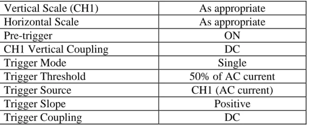
Table 3 – In-Rush Current Test – Oscilloscope Configuration
Vertical Scale (CH1) As appropriate
Horizontal Scale As appropriate
Pre-trigger ON
CH1 Vertical Coupling DC
Trigger Mode Single
Trigger Threshold 50% of AC current
Trigger Source CH1 (AC current)
Trigger Slope Positive
Trigger Coupling DC
7.8.3 Set the input AC voltage to the maximum specified input level using the adjustable transformer (Figure 2 Item #2).
7.8.4 Adjust the electronic load to the specified maximum output load current. If the power supply being tested has multiple DC voltage outputs adjust each DC output to the specified maximum output load current. Readjust the input AC voltage if it changed.
7.8.5 Turn off the AC input voltage to the DUT and allow all of the capacitors to fully discharge (>99% discharged). Consult the manufacturer’s data for the AC/DC power pack to determine the capacitor locations and normal voltages present within the power pack.
7.8.6 Verify that the DUT has zero DC output, and then turn on the AC supply. It is required that the AC supply voltage is applied to within ±1 milliseconds of the zero crossing point.
7.8.7 The oscilloscope should display a few impulses after the time the AC supply was turned on. These impulses are related to the in-rush current.
7.8.8 The in-rush current is the peak level of the highest of the in-rush impulses multiplied by the current to voltage ratio as stated on the current monitor. This ratio is typically 0.1 volt per ampere. Refer to Figure 5. Record the in-rush current.
Figure 5 – In-Rush Current
7.8.9 Holding the input AC voltage constant, adjust the electronic load(s) on the DC output(s) to the next load current(s) as desired. Readjust the input AC voltage if it changed. Repeat the measurements of 7.8.5 through 7.8.8 for each current. 7.8.10 Repeat 7.8.4 through 7.8.9 while adjusting the input AC voltage transformer in
steps, as desired, from the maximum to the minimum rated input levels for the AC voltage.
7.9 Start-up Time
7.9.1 Use the in-rush current set up as specified in section 7.8. Channel 1 should be monitoring the AC input current. Connect Channel 2 to the DC output voltage. 7.9.2 Configure the oscilloscope as outlined in the Table 4:
Table 4 – Start-up Time Test – Oscilloscope Configuration
Vertical Scale (CH1 & 2) As appropriate
Horizontal Scale As appropriate
Pre-trigger ON (>75%)
CH1 Vertical Coupling DC
CH2 Vertical Coupling DC
Trigger Mode Normal or Single
Trigger Threshold DC out minimum spec.
Trigger Source CH2 (DC output)
Trigger Slope Positive
Trigger Coupling DC
Record Length At maximum
7.9.3 Set the input AC voltage to the maximum specified input level using the adjustable transformer.
7.9.4 Adjust the electronic load to the specified maximum output load current. If the power supply being tested has multiple DC voltage outputs adjust each DC output to the specified maximum output load current. Readjust the input AC voltage if it changed.
7.9.5 Turn the AC supply “off” and allow time for the filter capacitors to fully discharge (discharge > 99%).
7.9.6 Find out where you are within cycle, to make sure you have zero crossing correct to within ±1 milliseconds. Turn the AC supply “on” and measure the time from the first in-rush current impulse to the point where the DC output voltage reaches the minimum operating specification. Refer to Figure 6. 7.9.7 Holding the input AC voltage constant, adjust the electronic load(s) on the DC
output(s) to the next load current(s) as desired. Readjust the input AC voltage if it changed. Repeat the measurements of 7.9.5 through 7.9.6 for each current. 7.9.8 Repeat 7.9.4 through 7.9.7 while adjusting the input AC voltage transformer
(Figure 2 Item #2) in steps, as desired, from the maximum to the minimum rated input levels for the AC voltage.
Figure 6 – Start-up Time
7.10 Power Factor
7.10.1 Connect the DUT to the setup as shown in Figure 2. Insert the 1 Ω power resistor (Figure 2 Item #12).
7.10.2 Set the AC voltage to the maximum specified input level using the adjustable transformer (Figure 2 Item #2).
7.10.3 Adjust the electronic load (Figure 2 Item #4) to the specified maximum output load current. If the power supply being tested has multiple DC voltage outputs, adjust each output to the specified maximum output load current. Readjust the input AC voltage if it has changed.
7.10.4 Using the power analyzer (Figure 2 Item #3) measure and record the power factor. If the power analyzer does not measure power factor, measure and record the AC input power, PIN(real), AC input voltage, VIN, and AC input current, IIN, and calculate the power factor from Equations 1 and 6.
7.10.5 Holding the input AC voltage constant, adjust the electronic load(s) on the DC output(s) to the next load current(s) as desired. Readjust the input AC voltage if it changed. Repeat the measurement of 7.10.4 for each current.
7.10.6 Repeat 7.10.3 through 7.10.5 while adjusting the input AC voltage transformer in steps, as desired, from the maximum to the minimum rated input levels for the AC voltage.
NOTE: The following set of tests is considered optional. They are unnecessary for power factor corrected supplies.
7.10.7 The previous series of tests were performed using the 1 Ω series resistor. The following steps will increase the resistance to simulate the coaxial loop resistance. Insert the 5 Ω power resistor (Figure 2 Item #13).
7.10.8 Set the AC voltage to the maximum specified input level using the adjustable transformer (Figure 2 Item #2).
7.10.9 Adjust the electronic load (Figure 2 Item #4) to the specified maximum output load current. If the power supply being tested has multiple DC voltage outputs, adjust each output to the specified maximum output load current. Readjust the input AC voltage if it has changed.
7.10.10Using the power analyzer (Figure 2 Item #3) measure and record the power factor. If the power analyzer does not measure power factor, measure and record the AC input power, PIN(real), AC input voltage, VIN, and AC input current, IIN, and calculate the power factor from Equations 1 and 6.
7.10.11Holding the input AC voltage constant, adjust the electronic load(s) on the DC output(s) to the next load current(s) as desired. Readjust the input AC voltage if it changed. Repeat the measurement of 7.10.10 for each current.