www.ijseat.com
Page 265
The Evolution of Microprocessor Chip: A historic overview of development
Waqar Ahmad Jang
1, Waseem Khan
1*, Sadawat Shah
1, Aadil Ahmad
11
Department of Computer Science, Abdul Wali Khan UniversityMardan, KPK, Pakistan
Email:
*[email protected], *[email protected]Abstract-In this paper we aredescribing the more interesting segments like, external structure of microprocessor chip(the birth of microprocessor) from silicon element becausemost of IT student does not have knowledge about the external structure. Also this paper presentsthe conventional silicon based computing technology for manufacturing of microprocessors but as we know that siliconreached to its upper limit of physical design therefore we also discussed the alternative of silicon in the future to makeprocessor more efficient with changing technology.
Keywords: Silicon Ingot, wafers, Exposure, Photo Resist, Etching, Electroplating, Binning,
I. INTRODUCTION
It is very crucial to design an electronic circuit in such a way that it will perform some very special function. In this circuit, transistors, diodes, capacitors and resistor are used which are small in size, they are combined together to make a chip which is made of silicon and are connected with one another through rope of aluminium [1]. It is commonly known as IC Chip or Microchip. In birthday musical card, the chips contains only few electronic component such as transistors and resistors, while Pentium processor contain about 800,000,000 (800 millions) transistors. When an IC goes towards more complexity then it is knowns as microprocessor.
The shape of silicon microprocessor chip is like a small rectangle, whose area is about 4 or 5 sq.cm. The size of these chips is regularly rising. In some cases, silicon is used as a base, on which chips is built. Silicon small rectangle chip consist of many layers. The lowermost part of it form the operative part (active), which is usually concerned with transistors, while the uppermost part is passive part and are concerned with wires. Around the boundary of chip there are pads, which are used to connect with outer world [2-5]. As size of microprocessor is
regularly rising, so number of layer is decreasing. The size of commercial microprocessor chips is about 65nm to 90nm. In 2007-08 the size of it was 45nm. Commonly on a silicon microprocessor chip we can fit up to 1000 million transistors, which are very large in number compared to the current processor. For comparison [6-11], we can make a logic gate from 2 to 10 transistors and memory circuit can be made from 1 to 12 transistors.
II. Manufacturing of Microprocessor chip
Silicon is 2nd most frequent chemical element on the earth surface after oxygen. It is about 25%. Especially in the Sand has a lot of SiO2 and is base element for the semiconductor manufacturing. First impure Silicon is purified in many steps to become semiconductor the resulting mono crystal is called Ingot [12-19]. Ingot is created from electronic grade silicon. It weight is about 100KG.one ingot is 99.99% pure.
Figure 1: Design of Ingot
www.ijseat.com
Page 266
printed circuits. Now a days Intel using 300mmwafers which decreased cost per chip. The blue fluid is depleted on the wafer while it twists is a photograph oppose wrap up. Amid turning, the wafer turns out to be slim and this is a use of the photograph oppose layer.
The photograph oppose completion is revealed to ultra violet light. This procedure step is like what happens to film material in a film camera the minute you press the shade catch. The photograph oppose completion that is presented to UV light will get to be dissolvable that demonstration like stencils in this procedure step A lens (center) diminishes the veil's picture to gets littler straightly imprinted on the wafer than the covers unique example. Albeit normally several chip are based on a solitary wafer, a microchip comprises of transistors. For controlling the stream of current in a PC chip, transistor goes about as a switch. Intel authority has delivered little transistors on which around 30 million can fit on the tip of pen. The photograph oppose is totally broken down by a dissolvable. The example of the photograph oppose is uncovered by the cover. The photograph oppose secure material that ought not be scratched away. Uncovered material will be expelled with chemicals [20-24]. After the scratching the photograph oppose is evacuated and the fancied shape gets to be unmistakable. There's photograph oppose (blue shading) connected uncovered and uncovered photograph oppose is being washed off before the following stride. The photograph oppose will secure material that ought not get particles embedded. Through a procedure called particle implantation (one type of a procedure called doping) the uncovered ranges of the silicon wafer are shelled with different compound polluting influences called Ions [25-29]. Particles are embedded in the silicon wafer to modify the route silicon in these ranges conducts power. At fast particles are shot on the wafer surface. At the point when electric field is connected, it quicken the particles to the rate of 300000km/h which is roughly equivalent to 185000mph. Photograph oppose will be disposed of after the particle implantation and the material that ought to have been doped has outsider iotas embedded at this point.
a. ReadyTransistor
Prepared transistor is near being done. Over the transistor three openings have been scratched into the protection layer (maroon shading). At that point copper is filled into these three openings which will make up the associations with different transistors. At this stage the wafers are put into a copper sulfate arrangement. Through a procedure called electroplating the copper particles are stored onto the transistor. The copper particles go from the positive terminal (anode) to the negative terminal (cathode) which is spoken to by the wafer.
On the wafer surface the copper particles settle as a dainty layer of copper as appeared in Figure 2. The abundance material is finished in the wake of electroplating. At this stage different metal layers are made to interconnect (think: wires) in the middle of the different transistors. How these associations must be "wired" is dictated by the engineering and plan groups that build up the usefulness of the individual processor (e.g. Intel Core i7 Processor). While PC chips look to a great degree level they may really have more than 20 layers to shape complex hardware [30-34]. On the off chance that you take a gander at an amplified perspective of a chip profoundly then you will see that an unpredictable system of circuit lines and transistors that resemble a modern multi-layered thruway framework.
Figure 2: Design of a Ready Transistor
Now this fraction of a ready wafer is being put to a first functionality test, and in this stage test patterns are fed into every single chip and the response from the chip monitored and compared to “the right answer”.
III. Wafer Sort Test
www.ijseat.com
Page 267
a. Wafer SlicingIn this piece of wafer is made called dies. When dies responds right answer to the test pattern it will be put forward for the next further step called packaging. The wafer pieces which have fault are discarded. An individual die has been cut out in the previous step (slicing). The die shown here is a die of an Intel Core i7 Processor.
Figure3 : Water Slice
b. Packaging
A processor is completed when die is substrated and the heat spreader is put together. The electrical and mechanical interface for the processor is built with green substrate to interact with the rest of the PC system. The silver heat spreader is a thermal interface where a cooling solution will be put on to [33-36]. This will keep the processor cool during operation.
c. Processor
Hundreds of steps are required for completed processor (Intel Core i7 Processor in this case). A microprocessor is the most complex manufactured product on earth. The world‟s best cleanest environment (a microprocessor lab) is required to make microprocessors. For key characteristics (are power dissipation and maximum frequency) processor is tested for the final test.
Processors with the same capabilities are put into the same transporting trays. Then after thatthe readily manufactured and tested processors (again Intel Core i7 Processor is shown here) either go to system manufacturers in trays or into retail stores in a box.
IV. Future Work
In this paper we statedabout the processor chip which is manufactured from the very commonly used element silicon. But we know thatsilicon is not enough for it, becauseconventional computing technology which is based on silicon has reached to its upper physical limits of Design complexity, processingpower, memory, energy consumption, density and heat dissipation, that is why what we need here is searching for new alternative computing medias, such as germanium which is used before, can overcome all these conventional computation problems. But to structure processor from these elements which are given below is a major challenge.Also different elements can be mixed together for achieving appropriate result.
a. The silicon alternative
There are some alternatives of silicon which can be used for transistors. These can be single elements or mixtures of the elements. The silicon is not only the element or substance which can be used for making the transistors. In the early days, the element germanium was also used for transistors. In here we are not suggesting that it should be used but it is an option of course, there are some other elements which are semimetal can be used as mixtures and better result can be achieved. Intel is experimenting on these semiconductors. Mixing these elements can give better outcome, because good properties of these elements can be fined tuned. Whereas by using only single element gives no such flexibility. Intel has more recently used the mixture of indium, arsenic and gallium and has referred, tantalizingly, to “very high performing devices” [37-39]. According to Stanford University carbon nanotubes made transistors have the potential to operate at 1THz.beyond this.
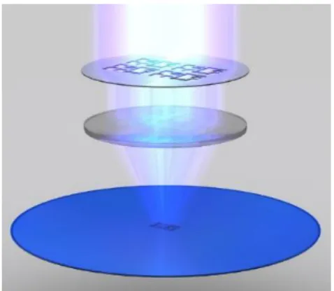
b. Light beam computing
www.ijseat.com
Page 268
technology. These computers also use binary valuesof „0‟ or „1‟ to represent information like traditional computers but at much faster speed as compared to the traditional computers. A table-top optical computer can process multiple operations at the same time with fast speed which is 100,000times faster than a traditional conventional computer. However, this technology (optical computers) may require one or two decade to bring for commercial use in markets.
c. Biological computing
Biological computing is the hot topic of science fiction. The artificial biological computing network is implemented by using analog electronics. In this DNA is used by the researchers. The human beings and all the living things relay on this complicated structure of the DNA molecules. Information is passed during the division of the cell and chemical reaction is the key factor. Because, data can be thought as sequence of bases and also chemical reaction of the DNA can be thought as processing, so there is potential of it that DNA can be used as processor. Traditional computing system can be replaced by biological computing. It provides an excellent way for computing.When DNA is filled to the test tube it consists of thousands of molecules. So DNA provides thousands of ways by which information can be routed in parallel. It might be strange using a test tube full of the chemicals but using biological material is even stranger of it. At the university of Florida neurons is used by the researchers from the rats as a replacement for the silicon chips. Here we are not suggesting that silicon should be replaced by biological computing but it needs to be considered. Chemical computer is a strange thing but processing of the data and its storage using DNA is possible.
V. Conclusion
In this paper we discuss about manufacturing of silicon chip in conventional method. Also we discussed that what the alternative of silicon for manufacturing of processor are, so we reached to the conclusion that presently silicon is still the best choice because of its efficient amount of availability and heat absorption.A processor is Integrated on a single chip is having many advantages. First, the components are interconnected closer, so by which communication is faster: in general, shorter communication paths are quicker. Faster clock rate occurs when the size of the processor shrinks, so do
certain unhelpful electronic properties (essentially capacitance) which enhance the processing speed. But chip size and transistor counts also have some restrictions. The processor has to fit in a small chip. Chips are, by nature, flat. Although there are wiring layers available, it is not a good idea to incorporate too many long wires (e.g. a few mm or more) into chips.Signals travelling down such wires may be unacceptably slow, resulting in lower clock rates
REFERENCES
[1]. Shazia Hassan, LIMITATION OF SILICON BASED COMPUTATION AND FUTURE PROSPECTS. [2]. Khan. F., Bashir, F. (2012). Dual Head Clustering
Scheme in Wireless Sensor Networks. in the IEEE International Conference on Emerging Technologies (pp. 1-8). Islamabad: IEEE Islamabad.
[3]. Syed Roohullah Jan, Farman Ullah, Hashim Ali and Fazlullah Khan, " Enhanced and Effective Learning through Mobile Learning an Insight into Students Perception of Mobile Learning at University Level", International Journal of Scientific Research in Science, Engineering and Technology(IJSRSET), Print ISSN : 2395-1990, Online ISSN : 2394-4099, Volume 2 Issue 2, pp.674-681, March-April 2016. URL : http://ijsrset.com/IJSRSET1622209.php [4]. Khan. F., Nakagawa. K. (2012). Cooperative
Spectrum Sensing Techniques in Cognitive Radio Networks. in the Institute of Electronics, Information and Communication Engineers (IEICE), Japan , Vol -1, 2.
[5]. Puthal, D., Nepal, S., Ranjan, R., & Chen, J. (2015). A Dynamic Key Length Based Approach for Real-Time Security Verification of Big Sensing Data Stream. In Web Information Systems Engineering–WISE 2015 (pp. 93-108). Springer International Publishing. [6]. M. A. Jan, P. Nanda, X. He, Z. Tan and R. P. Liu, “A
robust authentication scheme for observing resources in the internet of things environment” in 13th International Conference on Trust, Security and Privacy in Computing and Communications (TrustCom), pp. 205-211, 2014, IEEE.
[7]. Khan. F., Nakagawa, K. (2012). Performance Improvement in Cognitive Radio Sensor Networks. in the Institute of Electronics, Information and Communication Engineers (IEICE) , 8.
[8]. Puthal, D., Nepal, S., Ranjan, R., & Chen, J. (2015, August). DPBSV--An Efficient and Secure Scheme for Big Sensing Data Stream. InTrustcom/BigDataSE/ISPA, 2015 IEEE (Vol. 1, pp. 246-253). IEEE.
www.ijseat.com
Page 269
Internet Communication, Lecture Notes in Computer Science, pp. 154–167, Springer, Berlin, Germany, 2013.
[10].Khan. F., Kamal, S. A. (2013). Fairness Improvement in long-chain Multi-hop Wireless Adhoc Networks. International Conference on Connected Vehicles & Expo (pp. 1-8). Las Vegas: IEEE Las Vegas, USA. [11].Puthal, D., Nepal, S., Ranjan, R., & Chen, J. (2016). A
dynamic prime number based efficient security mechanism for big sensing data streams.Journal of Computer and System Sciences.
[12].M. A. Jan, P. Nanda, X. He and R. P. Liu, “Enhancing lifetime and quality of data in cluster-based hierarchical routing protocol for wireless sensor network”, 2013 IEEE International Conference on High Performance Computing and Communications & 2013 IEEE International Conference on Embedded and Ubiquitous Computing (HPCC & EUC), pp. 1400-1407, 2013.
[13].Jabeen. Q., Khan. F., Khan, Shahzad, Jan. M. A., Khan. S.A (2016). Performance Improvement in Multihop Wireless Mobile Adhoc Networks. in the Journal Applied, Environmental, and Biological Sciences (JAEBS), Print ISSN: 2090-4274 Online ISSN: 2090-4215
[14].Khan. F., Nakagawa, K. (2013). Comparative Study of Spectrum Sensing Techniques in Cognitive Radio Networks. in IEEE World Congress on Communication and Information Technologies (p. 8). Tunisia: IEEE Tunisia.
[15].Puthal, D., Sahoo, B., &Sahoo, B. P. S. (2012). Effective Machine to Machine Communications in Smart Grid Networks. ARPN J. Syst. Softw.© 2009-2011 AJSS Journal, 2(1), 18-22.
[16].Khan. F. (2014). Secure Communication and Routing Architecture in Wireless Sensor Networks. the 3rd Global Conference on Consumer Electronics (GCCE) (p. 4). Tokyo, Japan: IEEE Tokyo.
[17].M. A. Jan, P. Nanda, X. He and R. P. Liu, “PASCCC: Priority-based application-specific congestion control clustering protocol” Computer Networks, Vol. 74, PP-92-102, 2014.
[18].Khan. F. (2014). Throughput & Fairness Improvement in Mobile Ad hoc Networks. the 27th Annual Canadian Conference on Electrical and Computer Engineering (p. 6). Toronto, Canada: IEEE Toronto. [19].M. Usman, M. A. Jan, X. He and P. Nanda, “Data
Sharing in Secure Multimedia Wireless Sensor Networks,” in 15th IEEE International Conference on Trust, Security and Privacy in Computing and Communications (IEEE TrustCom-16), “accepted”, 2016,
[20].Khan. S., Khan. F., (2015). Delay and Throughput Improvement in Wireless Sensor and Actor Networks. 5th National Symposium on Information Technology: Towards New Smart World (NSITNSW) (pp. 1-8). Riyadh: IEEE Riyad Chapter.
[21]. Shahzad Khan, Fazlullah Khan, FahimArif, QamarJabeen, M.A Jan and S. A Khan (2016). “Performance Improvement in Wireless Sensor and Actor Networks”, Journal of Applied Environmental
and Biological Sciences, Vol. 6(4S), pp. 191-200,
Print ISSN: 2090-4274 Online ISSN: 2090-4215, TextRoad.
[22].Puthal, D., &Sahoo, B. (2012). Secure Data Collection & Critical Data Transmission in Mobile Sink WSN: Secure and Energy efficient data collection technique. [23]. M. Usman, M. A. Jan, X. He and P. Nanda, “Data
Sharing in Secure Multimedia Wireless Sensor Networks,” in 15th IEEE International Conference on Trust, Security and Privacy in Computing and
Communications (IEEE TrustCom-16), “accepted”,
2016,
[24].QamarJabeen, Fazlullah Khan, Muhammad Nouman Hayat, Haroon Khan, Syed Roohullah Jan, Farman Ullah, " A Survey : Embedded Systems Supporting By Different Operating Systems", International Journal of Scientific Research in Science, Engineering and Technology(IJSRSET), Print ISSN : 2395-1990, Online ISSN : 2394-4099, Volume 2 Issue 2, pp.664-673, March-April 2016. URL : http://ijsrset.com/IJSRSET1622208.php
[25].M. A. Jan, P. Nanda, X. He and R. P. Liu, “A Sybil Attack Detection Scheme for a Centralized Clustering-based Hierarchical Network” in Trustcom/BigDataSE/ISPA, Vol.1, PP-318-325, 2015, IEEE.
[26].Jabeen. Q., Khan. F., Hayat, M.N., Khan, H., Jan., S.R., Ullah, F., (2016) A Survey : Embedded Systems Supporting By Different Operating Systems in the International Journal of Scientific Research in Science, Engineering and Technology(IJSRSET), Print ISSN : 2395-1990, Online ISSN : 2394-4099, Volume 2 Issue 2, pp.664-673.
[27].Syed Roohullah Jan, Syed TauhidUllah Shah, Zia UllahJohar, Yasin Shah, Fazlullah Khan, " An Innovative Approach to Investigate Various Software Testing Techniques and Strategies", International Journal of Scientific Research in Science, Engineering and Technology(IJSRSET), Print ISSN : 2395-1990, Online ISSN : 2394-4099, Volume 2 Issue 2, pp.682-689, March-April 2016. URL : http://ijsrset.com/IJSRSET1622210.php
[28].Khan. F., Khan. F., Jabeen. Q., Jan. S. R., Khan. S., (2016) Applications, Limitations, and Improvements in Visible Light Communication Systems in the VAWKUM Transaction on Computer Science Vol. 9, Iss.2, DOI: http://dx.doi.org/10.21015/vtcs.v9i2.398
www.ijseat.com
Page 270
[30].M. A. Jan, “Energy-efficient routing and secure communication in wireless sensor networks,” Ph.D. dissertation, 2016.
[31].M. A. Jan, P. Nanda, X. He, and R. P. Liu,“A Sybil Attack Detection Scheme for a Forest Wildfire Monitoring Application,” Elsevier Future Generation Computer Systems (FGCS), “Accepted”, 2016.
[32].Syed Roohullah Jan, Faheem Dad, Nouman Amin, Abdul Hameed, Syed Saad Ali Shah, " Issues In Global Software Development (Communication, Coordination and Trust) - A Critical Review", International Journal of Scientific Research in Science, Engineering and Technology(IJSRSET), Print ISSN : 2395-1990, Online ISSN : 2394-4099, Volume 2 Issue 2, pp.660-663, March-April 2016. URL : http://ijsrset.com/IJSRSET1622207.php [33].
http://www.pcadvisor.co.uk/feature/tech-industry/processor-tech-of-future-3454672/
[34].http://www.quepublishing.com/articles/article.aspx?p= 482324&seqNum=5
[35]. http://science.opposingviews.com/silicon-used-computer-chips-1802.html
[36]. http://cacm.acm.org/magazines/2011/5/107702-the-future-of-microprocessors/fulltext
[37]. http://apcmag.com/picture-gallery-how-a-chip-is-made.htm/
[38]. http://atechjourney.com/future-of-microprocessor-in-the-next-couple-of-years.html/