Volume 3, Issue 2, 2016
73 Available online at www.ijiere.com
International Journal of Innovative and Emerging
Research in Engineering
e-ISSN: 2394 - 3343 p-ISSN: 2394 - 5494
Design SRAM Using FinFET -Review
Rashmi Vermaa, Prof. Rakesh Gajreb, Prof. Ankit AdesarabaPG Student, Uka Tarsadiya University, Bardoli, India b Assistant Professor, Uka Tarsaiya University, Bardoli, India
ABSTRACT:
As CMOS technology shows certain limitations on the devices, also as such the device is reduced more and more in the nanometer regime out of which power dissipation, current leakages, doping, and channel length is an important issue. FinFET is evolving to be a promising technology in this regard. In this the designing, modeling and optimizing the 6-T SRAM cell device is done. Intrinsic variations and leakage control in today’s world, is very difficult to achieve, So bulk-Si MOSFETs limit the scaling of SRAM.
Keywords:CMOS, FinFET, Spice, Read/Write Simulation
I. INTRODUCTION
As per Moore’s Law, the number of transistors in a unit chip area double every two years. But the existing technology of integrated circuit formation is posing some limitations to this law. CMOS technology shows certain limitations as the device is reduced more in the nanometer regime, out of which power dissipation, current leakages, doping, channel length is an important issue. FinFET is evolving to be a promising technology in this regard. This paper direct to analyze and compare the characteristics of CMOS and FinFET circuits at 45nm technology. Inverter circuit is implemented in order to analyze the basic characteristics such as noise margin, voltage transfer characteristics, leakage current and power dissipation. Further the efficiency of FinFET designed SRAM is increased, to reduce power as compared to CMOS using SRAM circuit. The predictive technology model (PTM) is used to simulate these CMOS and FinFET based SRAM which is a tentative model. Since the dimension of the MOSFETs are deduced considerably, it is necessary to know the potential of both technologies, with its available least dimensions..
It is found that 6-T FinFET-based SRAM cells designed with built-in feedback achieve significant improvements in the cell static noise margin (SNM) without area penalty, read/write in time analysis. Improvement in SNM (signal to noise margin) can be achieved in 6-T FinFET-based SRAM cells. Improvements in SNM as the 6-T cell, making them attractive for low-power, low-voltage applications. The long-channel-device-based SRAM cell is marginally robust than optimized SRAM; however, increased gate-edge tunneling and leakage parasitic capacitances degrade the power consumption and access time.
A. Overview Of FinFET
A multigate device refers to a MOSFET which incorporates more than one gate into a single device. Fin-type field-effect transistors (FinFETs) are more better substitutes for bulk CMOS at the nanoscale. Mostly FinFETs having double-gate control devices are preferred. In some experiment the two gates of a FinFET can either be shorted for higher performance, higher gain or independently controlled for lower leakage or reduced transistor count. These modifications gives rise to a rich design space. Since nanometre process technologies have advanced, chip density and operating frequency have increased, that makes power consumption in battery-operated portable devices a major concern.
74 replacement for the conventional bulk-CMOS devices.
In IG-FinFET, the top part of the gate is etched out, giving way to two independent gates. Because the two independent gates can be controlled separately, IG-mode FinFET offer more design options.
In LP-FinFET, in which the back-gate bias is tied to a reverse-bias voltage to reduce sub threshold leakage. FinFET offer the best drive strength in SG-mode. Ion reduces by about 60% in the IG and LP modes[1].
B. Dilemma Over CMOS based SRAM
1) While it is possible to scale the classical bulk-Si MOSFET structure down into the sub-20nm regime, SCE control requires heavy channel doping (>1018 cm-3) and heavy super-halo implants to control sub-surface leakage currents. As a result, carrier mobilities are gravely degraded due to impurity scattering and a high transverse electric field in the on state.
2) Furthermore, the increased depletion charge density results in a larger depletion capacitance hence a larger sub-threshold slope.And thus, for a given off-state leakage current specification, on-state drive current is degraded. Off-state leakage current is boosted due to band-to-band tunnelling between the body and drain.
3) Vt variability caused by unsystematic dopant fluctuations is another concern for nanoscale bulk-Si MOSFETs. Control of critical dimensions does not track its scaling, thus ratio of the standard deviation over the average increases. Designing large arrays must have design for 5 or more standard deviations. With increasing variations, it becomes difficult to guarantee near-minimum-sized cell stability for large arrays in embedded, low-power applications. Increasing transistor sizes, on the other hand, is counter to the fundamental reason for scaling in the first place – to increase density.
4) Access time is dependent on wire delays and column height. So to speed up arrays, segmentation method is commonly employed. With further reductions in bit-line height, the overhead area of sense amplifiers becomes substantial.
C. Challenges Overcome by FinFET
The FinFET has originally developed to manufacture of self‐aligned double‐gate MOSFETs. Also to address the need for improved gate control to suppress DIBL(Drain Induced Barrier Lowering), Subthreshold current and process‐induced variability for Lg < 25nm.Tri‐Gate and Bulk variations of the FinFET have been developed to improve manufacturability and cost. Multi‐gate MOSFETs provide a pathway to achieving lower power and/or improved performance. The double-gate FinFET offers distinct advantages for simultaneously suppressing the sub-threshold current and gate dielectric leakage current as compared to the traditional single-gate MOSFETs. The Random dopant fluctuation(RDF) is a form of process variation resulting from variation in the implanted impurity concentration. In MOSFET transistors, RDF in the channel region can alter the transistor's properties, especially threshold voltage. Thus Finfet technology are being carried out in order to suppress the dopant fluctuation which leads to the variation of threshold voltage.
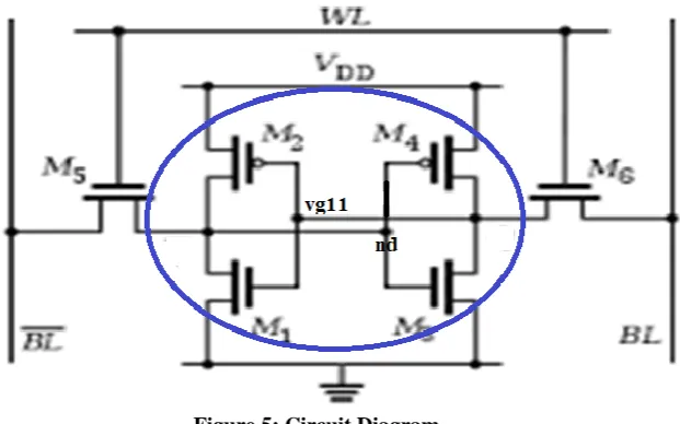
II. SRAM LAYOUT
The static random-access memories (SRAM) are most widely used, due to their high performance: microprocessors may contain up to 70% of SRAMs in transistor count or area[2]. The trend in the semiconductor market is to push for more integration and more size reduction: the development and optimization of a technological node is more and more difficult and expensive. The reduction in size of a SRAM circuit in coming nodes is nonetheless complex and it faces several limitations. The reliability of the SRAM bit-cell is degraded with ever smaller technologies and the device functionality is endangered. Designing SRAM circuits in CMOS 45nm requires technical and technological solutions to overcome the size reduction limitations, while insuring satisfactory functionality, with a guaranteed reliability so that it can be economically fabricated.
Volume 3, Issue 2, 2016
75 A. Result
Figure3 : Inverter output
Figure 4 : Butterfly curve
76
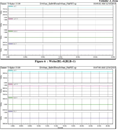
Figure 6 : Write(BL=0,BLB=1)
Figure 7 : Write(BL=1,BLB=0)
Volume 3, Issue 2, 2016
77
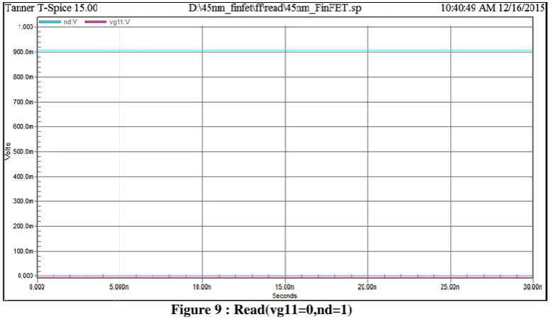
Figure 9 : Read(vg11=0,nd=1)
III.CONCLUSIONS
Based on above simulated results, I conclude that Sram Finfet of 45nm technology has higher SNM ratio as compared to CMOS based SRAM. Also the read and write operation of 1 and 0 is operated and performed and Data stored as per user requirement. Thus the analysis of read and write operation is performed perfectly and its very clear from graph.
ACKNOWLEDGMENT
I would like to express my deep sense of gratitude and indebtedness to my mentor Prof.Ankit Adesara and Prof.Rakesh Gajre for his invaluable encouragement, suggestions and support from an early stage of this dissertation and providing me extraordinary experience throughout the work. Above all, his priceless and meticulous supervision at each and every phase of work inspired me in innumerable ways.
REFERENCES
[1] Lourts Deepak A, Likhitha Dhulipalla, Dr. Cyril Prasanna Raj P,”Performance comparison of CMOS and FINFET based SRAM for 22nm Technology”,International Journal of Conceptions on Electronics and Communication Engineering Vol. 1, Issue. 1, Dec’ 2013; ISSN: 2357 – 2809
[2] Mugdha Sathe, Dr. Nisha Sarwade,” Performance Comparison of CMOS and Finfet Based Circuits At 45nm Technology Using SPICE”, Mugdha Sathe Int. Journal of Engineering Research and Applications ISSN : 2248-9622, Vol. 4, Issue 7( Version 2), July 2014, pp.39-43
[3] Brian Swahn and Soha Hassoun,” Gate Sizing: FinFET vs 32nm Bulk MOSFETs”, Tufts University Medford, MA 02155
[4] Prateek Mishra, Anish Muttreja, and Niraj K. Jha.” FinFET Circuit Design”
[5] Nahid Rahman, B. P. Singh,” Design of Low Power Sram Memory Using 8t Sram Cell”, International Journal of Recent Technology and Engineering (IJRTE) ISSN: 2277-3878, Volume-2, Issue-1, March 2013
![Figure 1: Types of FinFET[4]](https://thumb-us.123doks.com/thumbv2/123dok_us/8874661.1816135/1.595.151.447.621.734/figure-types-of-finfet.webp)
![Figure 2 : 6-T Sram[2]](https://thumb-us.123doks.com/thumbv2/123dok_us/8874661.1816135/2.595.192.424.606.768/figure-t-sram.webp)