International Journal of Innovative Research in Science, Engineering and Technology
An ISO 3297: 2007 Certified Organization Volume 6, Special Issue 5, March 2017
National Conference on Advanced Computing, Communication and Electrical Systems - (NCACCES'17)
24th - 25th March 2017
Organized by
C. H. Mohammed Koya
KMEA Engineering College, Kerala- 683561, India
A Highly Efficient SEPIC-Flyback Integrated
Converter as an LED Driver
Anusree M1, Sreeja E A2
M Tech Student, Department of Electrical and Electronics Engineering, FISAT, Angamaly, India1
Assistant Professor, Department of Electrical and Electronics Engineering, FISAT, Angamaly, India2
ABSTRACT: Light-emitting diodes (LEDs) have been widely used for various lighting applications. A high power
factor single-stage single-switch driver can be used to supply LEDs without using an electrolytic capacitor. By integrating the single-ended primary inductor converter (SEPIC) and flyback converter, LED driver could achieve nearly a unity power factor and low total harmonic distortion (THD). Since leakage energy is absorbed, there are no voltage spikes across the switch when it turns off. The SEPIC circuit is operated at discontinuous conduction mode (DCM) and there is only one active power switch which turns on under zero current switching (ZCS). Operating principles of the driver is discussed in detail. Simulation is done and results are presented to verify the theoretical analysis.
KEYWORDS: Single Ended Primary Inductance Converter (SEPIC), Flyback converter, Single-stage single-switch,
Discontinuous conduction mode (DCM), Power Factor Correction, Light-emitting diode (LED) Driver.
I. INTRODUCTION
LEDs have become increasingly common in our daily lives. With the advantages of superior longevity, fast response, small size and colour rendering, they are well suited to indoor and outdoor energy saving lighting applications, such as traffic lighting, displays, street lighting, decorative lighting and so on[1]. Since the package and costing technology are getting improved, the cost of LEDs decrease greatly, with a great potential to replace existing lighting sources such as fluorescent lamps. Being mercury free, it is less harmful for our environment.
To meet the power factor (PF) requirements, designers have to use power factor correction (PFC) techniques that improve the low frequency harmonic contents of power systems. Earlier methods for power factor correction (PFC), suggested a basic dc-dc converter [2]. But voltage ripple across the output capacitor is a major drawback in this method. To overcome this a second stage is required. A two stage LED driver is constructed by a dc-dc converter with a power factor correction (PFC) stage. The PFC stage achieves nearly a unity power factor and a low harmonic distortion, while the dc-dc converter provides a well regulated output.
and it can achieve a unity power factor. SEPIC provides an inherent input current filtering, so that an LC filter can be saved. An isolated single-stage single-switch PFC converter for LED driver is introduced which is composed of a single ended primary inductor converter (SEPIC) integrated with a flyback converter and no electrolytic capacitors are used.
Paper is organized as follows. Section II describes the operating principles and modes of operation of converter. The voltage and current across different components are presented. Section III presents simulation results showing the power factor corrected output of the converter. Finally, Section IV presents conclusion.
II.BASICOPERATINGPRINCIPLES
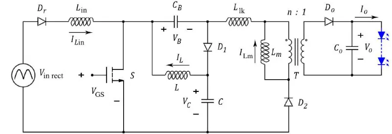
Fig. 1 shows the LED driver based on integrated SEPIC and flyback converter. There are six operating modes during one switching cycle in steady state condition. To simplify the circuit analysis, some assumptions are made:
1. All the components are ideal.
2. The capacitors C, CB and Co is large enough that their voltages are constant. 3. The switching frequency is much larger than line frequency
4. The transformer turns ratio is defined as n= Np/Ns
Fig. 1 Equivalent circuit diagram of the LED Driver
1. MODE 1 (t0 – t1)
When switch S turns ON, voltages Vin rect, VC, and VB are applied to the inductors Lin, L and Lm+ Llk respectively. The inductor current increases linearly from zero. The diodes D1 and D0 are reverse biased. Ts is the time period and D is the duty cycle. When switch S turns OFF, mode 1 ends.
2. MODE 2 (t1 – t2)
When switch S turns OFF, diodes D1 and D0 start conducting. Since D1 is conducting, Voltage across switch will get clamped. The voltage Vc – nV0 is applied to the inductor Llk inversely and its current decrease linearly to zero and hence leakage energy is absorbed. Diode D2 turns off at ZCS condition and mode 2 ends.
3. MODE 3 (t2 – t3)
During this mode, the voltages -(VB +VC + Vin rect), -VB and –nV0 are inversely applied across Lin, L and Lm respectively. Therefore current through the inductors decrease linearly and comes to zero. IL in reduces to zero first and mode ends.
4. MODE 4 (t3 – t4)
In this mode diodes D1 and D0 are still conducting and when IL becomes zero, diode D1 turns off under zero current switching condition.
5. MODE 5 (t4 – t5)
In this mode, current IL m is decreasing and no other inductor current is present. When ILm becomes zero, diode D0 turns OFF under ZCS condition.
6. MODE 6 (t5 – t6)
The main waveforms of the LED driver is presented in Fig 2.
Fig. 2 Main waveforms of the LED Driver
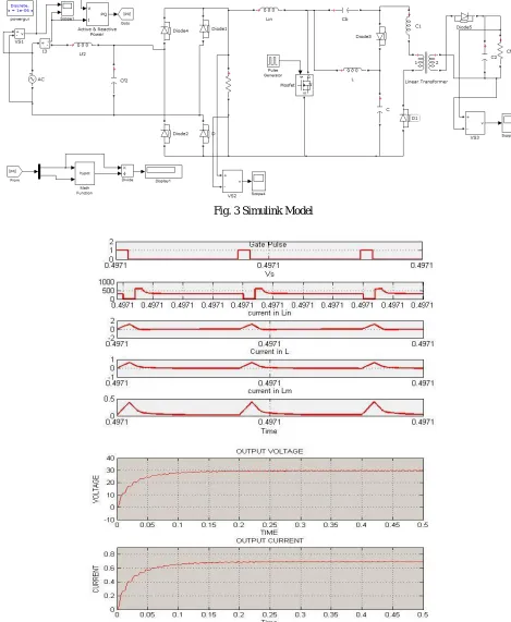
III.EXPERIMENTAL RESULTS
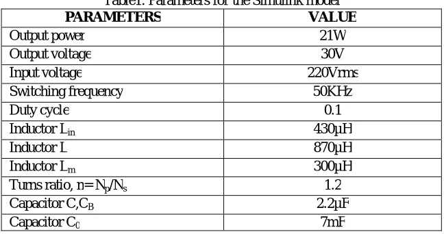
In order to verify the theoretical analysis, a Simulink model to supply a 21W/30 V LED module is implemented and required waveforms are obtained. Parameters of the model are shown in Table 1.
Table1. Parameters for the Simulink model
PARAMETERS VALUE
Output power 21W
Output voltage 30V
Input voltage 220Vrms
Switching frequency 50KHz
Duty cycle 0.1
Inductor Lin 430µH
Inductor L 870µH
Inductor Lm 300µH
Turns ratio, n= Np/Ns 1.2
Capacitor C,CB 2.2µF
Capacitor C0 7mF
REFERENCES
[1] J. Y. Tsao, “Solid state lighting: Lamps, chips, and materials for tomorrow,” IEEE Circuits Devices Mag., vol. 20, no.3, pp. 28-37, May/Jun.2004. [2] S. Dian, X. Wen, X. deng, and S. Zhang, “Digital control of isolated Cuk power factor correction converter under wide range of load
variation”, IET power electron, vol. 8, no.1, pp. 142–150, Jul. 2015.
[3] R. Redl and L. Balogh, “Design considerations for single-stage isolated power-factor-corrected power supplies with fast regulation of the output voltage,” in Proc. 10th IEEE Appl. Power Electron. Conf. (APEC), 1995, pp. 454-458
[4] H. J. Chiu et al., “A single-stage soft switching flyback converter for power factor correction applications,” IEEE Trans. Ind. Electron., vol. 57, no. 6, pp. 2187-2190, Jun.2010.