Vol. 3, Issue 10, October 2015
Noise Tolerant Current Mirror Footed
Domino Logic
Preetisudha Meher, Kamalakanta Mahapatra
Dept. of ECE, GITAM University, India
Dept. of ECE, NIT Rourkela, India
ABSTRACT: Domino logic design is preferable for designing high performance circuits because of its high operationalspeed and less number of transistor requirement as compared to the static CMOS logic style. But this logic is not widely accepted for all types of circuit implementations due to its less noise tolerance and charge sharing problems. A very small noise at the input of the dynamic logic can change the desired output of the circuit. Domino logic uses one static CMOS inverter at the output of dynamic node which is more noise immune and consuming very less power as compared to other proposed circuit. In this paper we have proposed a novel circuit for domino logic named as current mirror footed domino logic which has less noise at the output node and has very less power consumption as compared to the basic domino footed and footless logic styles. Low unity noise gain (UNG) is achieved by using the current mirror footer and also reducing leakage current when PDN is not conducting.
KEYWORDS: Dynamic logic, domino logic, Delay, current mirror, noise tolerance, power consumption, robustness, technology scaling,
I.INTRODUCTION
The rapid advancement of VLSI circuit is due to the increased use of portable and wireless systems with low power budgets and microprocessors with higher speed. To achieve this, the size of transistors and supply voltages are scaled with technology. Due to larger number of devices per chip the interconnection density increases. The interconnection density along with high clock frequency increases capacitive coupling of the circuit. Therefore noise pulses known as cross-talk can be generated leading to logic failure and delay of the circuit [1]. Again, when supply voltage is scaled the threshold voltage of the device needs to be scaled to preserve the circuit performance, which leads to increase in the leakage current of the device.
Due to high speed and low device count especially compared to complementary CMOS, dynamic-logic circuits are used in a wide veriety of applications including microprocessors, digital signal processors and dynamic memory [2]. Dynamic circuit contains a pull-down network (PDN) which realizes the desired logic functions. According to the basic theory, the dynamic logic circuit will precharge at every clock cycle. As the the clock signal frequency is high, the circuit is introduced with a lot of noise which consume extra power and slows the circuit.
Vol. 3, Issue 10, October 2015
II. DOMINO LOGIC STYLES
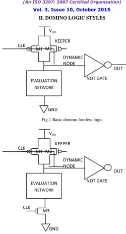
Fig.1 Basic domino footless logic
Fig.2 Basic domino footed logic
Fig. 1 is an example of footless domino gate. During the precharge phase when the clock is LOW, the pre-charging PMOS gets ON and the dynamic node is connected to the VDD and gets precharge to VDD. When clock goes high, the
evaluation phase starts and the output gets evaluated with the pull-down network and conditionally gets discharged if any one of the input is at logic 1. At the evaluation period, when all the inputs are at logic 0, the dynamic node should be at logic 1. But the wide fan-in NMOS pull-down leaks the charge stored in the capacitance at the dynamic node due to the subthreshold leakage. This is again compensated by the PMOS keeper, which aims to restore the voltage of the dynamic node. When a noise voltage impulse occurs at a gate input, the keeper may not be able to restore the voltage level of the dynamic node. The subthreshold leakage current is exponentially dependent upon VGS. So in the presence
of noise impulse the gate voltage increases, which leads to increase in VGS and the dynamic node gets wrongly
discharged.
To compensate the leakage current at the dynamic node a week transistor called keeper transistor is used. Keeper transistor prevents the charge loss and keeps the dynamic node at strong high when PDN is OFF. In the first domino
OUT M1 M2
M3 EVALUATION
NETWORK
VDD
GND KEEPER
CLK CLK
DYNAMIC NODE
NOT GATE OUT M1 M2
EVALUATION
NETWORK
VDD
GND KEEPER CLK
DYNAMIC NODE
Vol. 3, Issue 10, October 2015
proposal [3] the gate of the keeper transistor is tied to ground, therefore the keeper is always on. If at the beginning of evaluation the pull-down network (PDN) turns on, the dynamic node tends to discharge through the PDN. However, the keeper is injecting charge to the dynamic node as it is always on. This is called contention. Furthermore, a potential DC power consumption problem is generated. To alleviate the potential DC power consumption problem a feedback keeper was proposed in [4, 5].
Fig. 2 demonstrates the domino footed domino logic. This is the advances version of the footless domino as it contains a footer transistor in the circuit. This footer transistor acts as the stacking transistor. (Stacking effect - Subthreshold leakage current flowing through a stack of series-connected transistors reduces, when more than one transistor in the stack is turned off. This effect is known as the stacking effect).
As noise of domino gates is always more important in domino CMOS logic than the area, energy dissipation and delay issues, so recently several techniques have been proposed [6,7] to reduce the noise of dynamic circuits. All the techniques have reduced the noise sensitivity but there are many drawbacks with area, power dissipation and delay.
III. CURRENT MIRROR FOOTED LOGIC
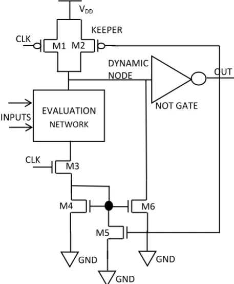
The proposed current mirror footed circuit technique is illustrated in Fig. 3. In this circuit M1 is the precharge
transistor which inputs the clock signal (CLK). M2 is the keeper transistor which prevents the charge loss and keeps the
dynamic node at strong high when PDN is OFF. M3, M4, M5 and M6 are the four footer transistors which play a great
role in making the circuit noise tolerant and consume lesser power as compared to the basic domino circuit techniques. The transistors M3 and M4are added to provide stacking effect to the circuit, which can reduce the leakage current
during the evaluation phase. However, the evaluation delay of the circuit can be increased by increasing the size of the stack in the footer. To reduce this evaluation delay, a current mirror transistor (M6) is added in parallel to the evaluation
network of the current mirror footed domino circuit technique. Which can increase the discharging current the inputs is high. Transistor M5 acts as a feedback path fromthe output node to the gates of current mirror M4 and M6. The source
of M5 is grounded. As a result, in presence of noises at inputs M9 turns off the current mirror path and stops discharging
the dynamic node.
Fig. 3 Current mirror footed domino logic
CLK
OUT M1 M2
EVALUATION
NETWORK
VDD
GND KEEPER CLK
DYNAMIC NODE
NOT GATE
GND
GND M3
M4
M5
Vol. 3, Issue 10, October 2015
The proposed circuit worksas follows:
In the charge phase, when the clock is low, the circuit is in the charge mode, and the dynamic node gets pre-charge to high. When the footer transistor(M3)is turned off a verysmall leakage current passes through M4 pulling an
eligible current from the dynamic node.
In the evaluation phase when the clock is high, this circuit show significantly improved noise immunity due to the stacking effect provided by the transistor M4.
When the clock is high, if all the inputs are zero, the setwostacked NMOS transistors M3 and M4 substantially
reduce the sub threshold current.
However, when at least one of the inputs switches to high, the mirror transistor pulls large current from the dynamic node resulting in a high to low transition on the dynamic node. In this case, output of the gate goes high turning on the NMOS transistor M5 disabling the current mirror. For the rest of evaluation phase current mirror remains
OFF.
IV. SIMULATED RESULTS
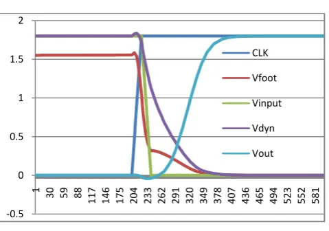
Fig. 4 Simulated waveform of proposed scheme
Fig. 4 illustrates the simulated waveform of proposed scheme. It includes the transient voltage waveform of CLK, footer voltage, input voltage, dynamic node voltage and output voltage. This is the simulated output in the evaluation period of the clock. In the evaluation period, when one of the inputs makes a transition from 1 to 0, the dynamic node also gets a transition from 1 to 0 and simultaneously the output changes from 0 to 1.
V. COMPARISON RESULTS WITH OTHER LOGIC TECHNIQUES
UNITY NOISE GAIN
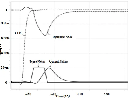
Unity noise gain (UNG) describes a method of leakage measurement of the circuit. For robustness measurement, identical noise pulses were applied to all inputs in the evaluation phase, and the amplitude of the noise at the output of the static OR gates were measured as shown in Fig. 5. While applying noise pulses, the pulse were kept constant at 30 ps (typical gate delay at 180-nm technology) and the amplitude of the output noise was observed for different amplitudes of the input noise. The metric we used for leakage and noise robustness comparison is the unity noise gain (UNG), defined as the amplitude of the input noise that causes the same amplitude of noise at the output [15] UNG (2). We used a pulse noise to simulate cross-talk type of noise at the input. The effective noise depends on both the amplitude and duration of the noise pulse. The input noise level can be increased by increasing either the noise pulse duration or amplitude. In our experiments, we change the input noise level by changing its amplitude.
UNG = {Vnoise; Vnoise = Vout}
-0.5 0 0.5 1 1.5 2
1 30 59 88
117 146 175 204 233 262 291 320 349 378 407 436 465 494 523 552 581 CLK
Vfoot
Vinput
Vdyn
Vol. 3, Issue 10, October 2015
Fig. 5 UNG-delay curves for wide dynamic OR gates
Table 1 and Fig. 6 compares the UNG of the proposed circuit with the footed and footless domino circuits in tabular form and histogram form respectively. In both the cases the fan in of the OR gate varied from 2 to 32 and the UNG were calculated in the same environment for all the logics and found that the proposed current mirror is having high noise tolerance capacity as compared to the other two schemes. The circuits were being simulated with UMC 90 nm technology using cadence spectre. The simulated voltage is 1.8 V and the operational frequency is 200 MHz simulated in 27OC.
Table 1 Unity Noise Gain Comparison with basic circuits under Same Delay (UNG Normalized To V = 1V)
Fan-in Basic Domino Footless Basic Domino Footed Proposed Scheme
2 436 567 800
4 409 530 810
8 376 493 823
16 332 448 825
Vol. 3, Issue 10, October 2015
Fig. 6 UNG comparison under Same Delay (UNG numbers normalized to V = 1V) shown in histogram formfor OR gate varying from 2 input to 32 input
Table 2 UNG and performance measurement with different width of M6 for the proposed circuit at 90 nm technology for an input of 2
Width of M6 UNG (normalized to VDD=1V) Power Delay
0.12 um 800 1.34 E-8 3.11 E-10
0.18 um 795 2.55 E-8 2.66 E-10
0.24 um 796 2.61 E-8 1.75 E-10
0.30 um 791 2.78 E-8 1.79 E-10
0.36 um 790 3.12 E-8 1.65 E-10
0.42 um 790 3.22 E-8 1.50 E-10
Transistor M6 plays a crucial role in terms of leakage and performance of gate in the proposed scheme. Its high
width improves the performance by making the speed more but penalty paid is slightly less noise robustness and more power consumption. Table 2 shows the UNG, power and delay measurements for various widths of M2 which was
simulated with UMC 1.8 V and 90 nm technology. Table 3 demonstrates the powerdissipation for the proposed circuit and the basic domino circuits simulated for 2 input OR gate in 1.8 V with UMC 90 nm technology using cadence spectre. It shows that this scheme also reduces the power dissipation of the circuit dramatically.
Table 3 Power comparison for different circuit techniques simulated for 2 input OR gate
Logic styles Power in um
Basic footless 93.9
Basic footed 40.6
Vol. 3, Issue 10, October 2015
VI.CONCLUSION
In this paper, a noise tolerant current mirror CMOS domino logic circuit technique has been proposed, which also have less power consumption. The simulation work was done with 180 nm and 1.8 V CMOS process. The results show that the proposed scheme is highly noise tolerant. It shows UNG i.e. unity noise gain nearly double to the basic CMOS domino circuits. Proposed circuit also shows less power consumption i.e. nearly 10 to 20 % of power saving as compared to the previous footed and footless domino logics. Also the circuit is flexible for wide variety of dynamic logic styles and adequate for large fan-in gates.
REFERENCES
[1]F. M. Hernandez, M. L. Aranda and V. Champac, “Noise tolerant improvement in dynamic CMOS logic circuit”, IEEE Proc.-Circuits Devices Systems, Vol 153, No. 6, Dec 2006, pp.. 565-573
[2] H.L. Yeager et al, “Domino Circuit Topology”, U. S. Patent 6784695, Aug. 31, 2004.
[3]R. H.Krambeck, C. M.Lee, and S. Law, “High-speed compact circuits with CMOS”, IEEE J. Solid-State Circuits, 1982, 17, (3), pp. 614–619 [4]V.G.Oklobdzija, and R. K. Montoye, “Design-performance tradeoffs in CMOS domino logic”. Proc. IEEE Conf. on Custom Integrated Circuits,
May 1985, pp. 334–337
[5]V.G. Oklobdzija, and R.K.Montoye,”Design-performance tradeoffs in CMOS-domino logic”, IEEE J. Solid-State Circuits, 1986, 21, (2), pp. 304–306
[6]M. H.Mahmoodi, K.Roy: „Diode-footed domino: a leakage-tolerant high fan-in dynamic circuit design style‟, IEEE Trans. Very Large Scale Integr. Syst., 2004, 51, (3), pp. 495–503
[7]F. Frustaci, P.Corsonello,G. Cocorullo: „A new noise-tolerant dynamic logic circuit design‟, IEEE Ph.D. Research in Microelectronics and Electronics, PRIME 2007, Bordeaux, France, July 2007, pp. 61–64
[8] F. Tang, K. Zhu, Q. Gan and J. G. Tang, “Low-noise and power dynamic logic circuit design based on semi-dynamic logic”, Anti-counterfeiting, Security and Identification, 2008. ASID 2008. 2nd International Conference on 20-23 Aug. 2008, pp 20-23
[9]A. Alvaizdpoul, P. L. Edefors and C. Sveizsson, “A Leakage-Tolerant Multi-Phase Keeper For Wide Domino Circuits,” Proceedings of ICECS '99. The 6th IEEE International Conference on Electronics, Circuits and Systems, pp.209, 1999.
[10] K. S. Yeo, K. Roy, “Low-voltage low-power voltage subsystems” Tata Mc-Graw-Hill edition 2009. [11]http://ptm.asu.edu/modelcard/2006/45nm_bulk.pm
[12]R. J.H. Sung, D. G. Elliott, “Clock-Logic Domino Circuits for High-Speed and Energy-Efficient Microprocessor Pipelines,” IEEE Transactions on Circuits and Systems II: Express Briefs, Vol.54(5), pp.460, May 2007.
[13] V. Sharma, W.K. Al-Assadi, “Analysis and Modeling of Crosstalk Noise in Domino CMOS Circuits,” IEEE Region 5 Technical Conference, pp.374, April 2007.
[14] S. Jia, F. Liu, J. Gao, L. Liu, X. Wang, T. Zhang, Z. Chen, L. Ji, “A 64-bit lookahead carry chain in Inverted-Domino logic,” IEEE Conference on Electron Devices and Solid-State Circuits, pp.281, Dec. 2003.