Three phase to single phase current fed high
step up ac-dc matrix converter based on CWVM
Peerila Premsagar
1& Ch. Mounika
21
PG Scholar, Dept of EEE(Power Electronics), Pathfinder Engineering College, Thimmapur,
Hanamkonda, Warangal, TS, India.
2
Assistant Professor, Dept of EEE, Pathfinder Engineering College, Thimmapur, Hanamkonda,
Warangal, Hyderabad, TS, India.
Abstract: -
A single-phase step-up ac–dc matrix converter based on Cockcroft–Walton CW) voltage
multiplier is explained in this paper. Here we are using a four bidirectional- switch matrix converter in
between the CW circuit and ac source, the modern topology gives high quality of line conditions, adjustable
output voltage, and low output ripple. The proposed matrix converter is operated with two independent
frequencies. One of the frequencies is associated with Power Factor Correction (PFC) control, and the
other frequency is to set the matrix converters output frequency. Here we are simulated 50V/12W
converter for measurement and analysis. The measured system efficiency and power factor is improved and
output voltage ripple is reduced at full load condition.
Index Terms
: -
Cockcroft–Walton voltage multiplier (CW), high step-up ac–dc converter, power factor
correction (PFC).
I.INTRODUCTION
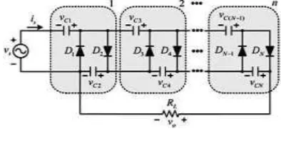
High voltage dc power supplies are commonly used in science, military, industries, medicine, such as test equipment, X-ray systems, dust-filtering, insulating test, and electrostatic coating [1]–[3]. Using the advantages of low voltage stress on the diodes and capacitors, high voltage ratio, compactness, and cost efficiency, the conventional Cockcroft–Walton (CW) voltage multiplier is commonly used for high-voltage dc applications. A conventional CW voltage multiplier is shown in Fig. 1. The well-known CW voltage multiplier is made by joining a number of diode–capacitor ladder stages with each stage containing two capacitors and two diodes. Theoretically, an n-stage CW voltage multiplier dc output voltage is equal to the value of 2n times of the magnitude of the ac voltage source under no-load condition. Due to non ideal characteristics of the circuit components the dc output voltage is practically less than the theoretic value [1], [3], [4]. Some drawback of CW multiplier is, under heavy-load condition, the CW multiplier intrinsically presents not only poor output voltage regulation but also high output ripple with line frequency. In some applications, for getting higher voltage gain we use line frequency transformers with high step-up ratio to cooperate with the CW voltage multiplier. However, sourced by the utility ac source, the transformers lead to inefficiency of bulk and cost, and the ripple problem still
topology, all capacitors in the voltage multiplier had identical voltage rating. Moreover, some non isolated high step up dc–dc converters with low-voltage dc input were proposed for renewable energy applications [16]– [18].
Figure 1: Conventional Cockcroft-Walton voltage multiplier
II.PRINCIPLE OF OPERATION OF THE
CONVERTER
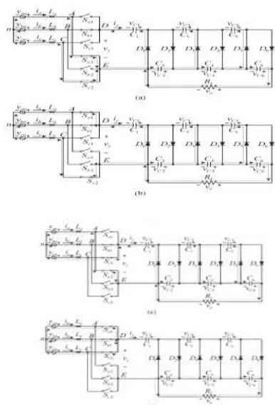
Fig.2 shows the proposed converter, which is supplied by a three-phase ac source, and the phase voltages are denoted by van, vbn, and vcn, respectively. A three-phaseto- single-phase matrix converter, which is composed of three boost inductors (La, Lb, and Lc) and six bidirectional switches (Sa1, Sb1, Sc1, Sa2, Sb2, and Sc2), is inserted between the ac source and a conventional N/2-stage CWVM circuit, where N is an even integer. Two antiseries insulated-gate bipolar transistors form one bidirectional switch, as shown in the bottom left part in Fig. 3.2.1. The six bidirectional switches are divided into two parts, namely, the upper part (Sa1, Sb1, and Sc1) and the bottom part (Sa2, Sb2, and Sc2). According to the first subscripts of the switches, the left terminals of the switches connect to the relative ac sources through three boost inductors. The three right terminals of the upper-part switches connect to the upper terminal D of the CWVM, whereas the three right terminals of the bottom-part switches connect to the bottom terminal E of the CWVM. For simplicity, the derivation of the mathematical model is divided into two parts, namely, the ac-side part and the CWVM, which are separated by terminals D and E.
Fig.2. Configuration of the proposed converter with an N/2-stage CWVM
A. Mathematical Model of the Circuit in the AC Side
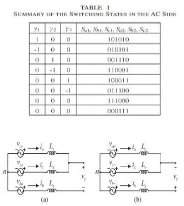
Assuming that the PFC technique is properly applied to the proposed converter and that the circuit operates under continuous conduction mode (CCM), there are eight switching states of the six bidirectional switches, which are summarized in Table I, in which three auxiliary variables γ1, γ2, and γ3 are used to determine the connection between the three input lines and the voltage multiplier. Two equivalent circuits corresponding to two of the eight switching states are shown in Fig. 3.2, and the other six can be easily obtained. It has to be noted that, in Fig. 3.2, vγ represents the terminal voltage of the CWVM, whose value is determined by the combination of the capacitor voltage(s) of the CWVM according to diode-conducting states. Consequently, the ac-side mathematical model of the proposed converter is given as
where Ls = La = Lb = Lc is the inductance of the boost inductor; vγ is the terminal voltage of the CWVM; and γa, γb,
and γc are defined as
where the current iγ is the current feeding into the CWVM and can be deemed a pulse-form current source.
Fig 3. Two circuit states of the proposed converter in ac source side. (a) Sa1, Sb2, and Sc1 are turned on. (b) Sa2, Sb1, and Sc2 are turned on.
B. Steady-State Operation of the Proposed Converter
In this paper, the CWVM is operated and analyzed by current-fed method, in which the matrix converter generates the frequency and adjustable-amplitude current, i.e., iγ, and feeds it into the CWVM. Before analyzing, some assumptions are made, as follows [27].
1) All of the circuit elements are ideal, and there is no power loss in the system.
2) All of the capacitors in the N/2-stage CWVM are large enough; thus, the voltages across them are equal and ripple free, except the first capacitor, whose voltage is one half of the others.
3) The boost-type matrix converter operates in CCM and under steady-state condition.
4) When one of the boost inductors transfers the storage energy to the CWVM, i.e., iγ _= 0, only one of the diodes in the CWVM will conduct.
5) The three-phase ac source is balanced and undistorted.
6) To avoid the open circuit of the inductors, a safe commutation technology provides enough overlap of the trig signals between the relative switches. Analysis of circuit will ignore the safe-commutation states for simplicity.
III.MODES OF OPERATION
1) Mode 1 :In this state, Sa1(Sa2) and Sc1(Sc2) turn off (on). The two boost inductors La and Lc and the two input phase voltages van and vcn transfer energy to the CWVM through one of the odd diodes in the CWVM. Thus, iγ = ib = −(ia + ic) < 0 and vγ = −Vo/N, and the equations relative to ia and ic are given as
To ensure boost operation, the dc output voltage has to meet the following condition:
2) Mode 2: In this state, Sa1(Sa2) turns on (off), and Sc1(Sc2) turns off (on). The boost inductor La is charged by van, and the boost inductor Lc and the phase voltage vcn transfer energy to the CWVM through one of the odd diodes. Thus, iγ = −ic, vγ = −Vo/N, and the equations relative to ia and ic are given as
4) Mode 4: In this state, Sa1(Sa2) and Sc1(Sc2) turn on (off). The boost inductors La and Lc are charged by van and vcn, respectively. Due to no current path, iγ = 0, and all diodes in the CWVM are off; thus, all even capacitors C6, C4, and C2 are in series and supply power to load RL, whereas the odd capacitors C5, C3, and C1 are floating. The equations relative to ia and ic are given as
For the second half of sector I, which is also denoted as mode 2, Sb2(Sb1) always turns on (off), and there are four circuit states in this mode as well. The operation of these four states is similar to that of mode 1, except that iγ and vγ have opposite polarities. Table II summarizes the switching pattern of the six bidirectional switches and the relative circuit characteristics in sector I. From this table, it can be seen that the switching states of the switch pairs (Sa1, Sa2), (Sb1, Sb2), and (Sc1, Sc2) are complementary in sector I, and this rule is also available for the operation in other five sectors. Consequently, through a similar process, the circuit operation and switching patterns can be obtained. The simulated waveforms of iγ and vγ are shown in Fig. 3.3(a) and (d), respectively; and the corresponding switching signals of the three upper-part switches are shown in Fig. 3.3(e). It can be seen that iγ changes polarity once in each
sector, i.e., the frequency of iγ is six times as high as the line frequency in this case; and in this paper, the frequency of iγ is defined as the alternation frequency. The alternation frequency is determined by the number of mode swaps in one sector, which can be implemented by changing the conduction state of Sb1 in sector I and Sa1 in sector II, etc. Obviously, higher alternation frequency leads to smoother ripple, and the ripple factor of the dc output will be significantly improved.
Fig. 4. Four circuit states of the proposed converter in mode 1 of sector I. (a) State 1. (b) State 2. (c) State 3.
(d) State 4
IV.CONTROL STARTAGY
which a phase-locked loop (PLL) subblock is used to generate the phase angle θ. Referred from the required equation for the PLL is given as
where vqs and vds are the voltages of the static reference frames ds and qs, respectively. Then the voltages vqs and vds are transformed to the voltages of the synchronous rotating frame vqr and vdr, respectively, by
where θ is the angle between the static reference frame and the rotating reference frame. The obtained angle θ and Sfa, which is a square wave signal relative to the alternation frequency, are used to generate the sector and mode signals SSec and SM according to the rule listed in Table IV.
Fig. 5. Control block diagram. (a) Control block of the proposed converter. (b) Block diagram of the
sector/mode generator.
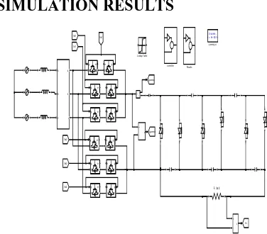
V. SIMULATION RESULTS
Fig.6. Circuit model design for proposed conveter
Fig.7.Voltage Source waveforms
Fig.8.Waveforms for current source
Fig.9voltage and current waveforms at current fed converters
Discrete, Ts = 5e-005 s.
powergui controller v + -v + -A B C a b c Results R load Lookup Table g m C E g m C E g m C E g m C E g m C E g m C E g m C E g m C E g m C E g m C E g m C E g m C E Igamma Vgamma Vo Sc2 Sb2 Sa2 Sc1 Sb1 Sa1 i +
-1 1.1 1.2 1.3 1.4 1.5 1.6 1.7 1.8 1.9 2
-200 0 200
Va
1 1.1 1.2 1.3 1.4 1.5 1.6 1.7 1.8 1.9 2
-200 0 200
Vb
1 1.1 1.2 1.3 1.4 1.5 1.6 1.7 1.8 1.9 2
-200 0 200
Time
Vc
1 1.1 1.2 1.3 1.4 1.5 1.6 1.7 1.8 1.9 2
-2 0 2x 10
-3
Ia
1 1.1 1.2 1.3 1.4 1.5 1.6 1.7 1.8 1.9 2
-2 0 2x 10
-3
Ib
1 1.1 1.2 1.3 1.4 1.5 1.6 1.7 1.8 1.9 2
-2 0 2x 10
-3
Time
Ic
1 1.1 1.2 1.3 1.4 1.5 1.6 1.7 1.8 1.9 2 -2
-1.5 -1 -0.5x 10⁻⁵
V
ga
m
m
a
1 1.1 1.2 1.3 1.4 1.5 1.6 1.7 1.8 1.9 2 -4
-2 0 2 4x 10⁻¹⁰
Time
Ig
am
m
CONCLUSION
In this paper, a three-phase-to-single-phase current-fed high step-up ac–dc matrix converter based on CWVM without a line and high-frequency step-up transformer has been presented to obtain high voltage gain. By using current hysteresis control to implement PFC, the proposed converter offers almost unity PF with low THDi at the ac mains; meanwhile, the matrix converter provided an adjustable-frequency and adjustable amplitude current to feed the CWVM to regulate the dc output and smooth ripple voltage. The programmable alternation frequency can be used to improve the ripple effect according to the application requirement. However, too much higher alternation frequency deteriorates the performance of the system; thus, the highest alternation frequency should be limited. The circuit operation, control strategy, and design considerations of the proposed converter were detailed in this paper. Two simulation cases were conducted to evaluate the performance of the proposed converter. A 500-W prototype, including the power stages and a DSP-based controller (TMS320F28069), was established for measurement and test. Both simulation and experimental work were conducted, and their results demonstrated the validity and the good performance of the proposed converter. Compared with conventional CWVM, the proposed converter sourced by a three-phase source is quite suitable for high-voltage and high-power applications.
REFERENCES
[1] Y. Xue, L. Chang, S. B. Kjaer, Jr., J. Bordonau, and T. Shimzu, “Topologies of single-phase inverters for small distributed power generators: An overview,” IEEE Trans. Power Electron., vol. 19, no. 5, pp. 1305–1314, Sep. 2004.
[2] L. S. Yang, T. J. Liang, and J. F. Chen, “Transformerless dc–dc converters with high step-up voltage gain,” IEEE Trans. Ind. Electron., vol. 56, no. 8, pp. 3144–3152, Aug. 2009.
[3] W. Li and X. He, “Review of nonisolated high-step-up dc/dc converters in photovoltaic grid-connected applications,” IEEE Trans. Ind. Electron., vol. 58, no. 4, pp. 1239–1250, Apr. 2011.
[4] D. Zhou, A. Pietkiewicz, and S. Cuk, “A three-switch high-voltage converter,” IEEE Trans. Power Electron., vol. 14, no. 1, pp. 177–183,Jan. 1999.
[5] J. Tanaka and I. Yuzurihara, “The high frequency drive of a new multistage rectifier circuit,” in Proc. IEEE
Power Electron. Spec. Conf., Apr.1988, pp. 1031–1037.
[6] J. F. Chen, R. Y. Chen, and T. J. Liang, “Study and implementation of a single-stage current-fed boost PFC converter with ZCS for high voltage applications,” IEEE Trans. Power Electron., vol. 23, no. 1, pp. 379–386, Jan. 2008.