ISSN (Print) : 2320 – 3765 ISSN (Online): 2278 – 8875
I
nternational
J
ournal of
A
dvanced
R
esearch in
E
lectrical,
E
lectronics and
I
nstrumentation
E
ngineering
(An ISO 3297: 2007 Certified Organization)
Website: www.ijareeie.com
Vol. 6, Issue 12, December 2017
Sequential Circuit Elements Using Reversible
Logic Gates with MUX
Prof.Venugopal B K , Rashmi Jakka
Associate Professor, Dept. of Electronics and Communication Engineering, University Visvesvaraya College of
Engineering, Bangalore, India
PG Student, Dept. of Electronics and Communication Engineering, University Visvesvaraya College of Engineering,
Bangalore, India.
ABSTRACT: The reversible logic circuits are becoming popular in the design of low power digital circuits. The researchers building vital circuits required in advanced computing machines using reversible logic including DNA computing, optical information processing, quantum computation and nanotechnology. The sequential circuits are complex than combinational circuits since the output depends not only on present input but on the past input. It is proposed to replace basic gates with reconfigurable gate multiplexer to reduces delay. The proposed design of reconfigurable logic will improve h throughput area, power, and delay and garbage outputs. The modules has been coded with Verilog and simulated on ISE Design suite 14.7 and Modelsim.
KEYWORDS: Reversible logic gates, quantum computers, sequential circuits, latches, flip flops,mux.
I.INTRODUCTION
The Reversible logic is drawing attention due to its ability to reduce the power dissipation. According to Landauer’s principle, the loss of one bit of information dissipates kTln2 joules of energy [1]. Later Bennett, in 1973, claimed circuits built using reversible circuits can avoid kTln2 joules of energy dissipation in a circuit [2]. The integrated circuit would continue to improve unit cost by a factor of 2, every 18 months according to Gordon Moore[3], shrinking the dimensions on integrated structures increase the speed for the same power per unit area. The power dissipation in present day computing devices are becoming very high as more and more components are getting packed onto the chip. The future technology would use reversible gates to reduce power[4]. Many people pursuing research in the area of reversible logic. Computers based mainly on reversible logic operations can reuse a fraction of the signal energy that theoretically can approach arbitrarily near to 100% as the quality of the hardware is improved[5].Like conventional digital circuits reversible logic circuits are classified into reversible combinational and reversible sequential circuits. Any arbitrary computational work and logic function can be realized using reversible in the same way it is done with conventional logic circuits. It is possible to build sequential computer with zero internal power dissipation using invertible logic gates[6].
ISSN (Print) : 2320 – 3765 ISSN (Online): 2278 – 8875
I
nternational
J
ournal of
A
dvanced
R
esearch in
E
lectrical,
E
lectronics and
I
nstrumentation
E
ngineering
(An ISO 3297: 2007 Certified Organization)
Website: www.ijareeie.com
Vol. 6, Issue 12, December 2017
II.BASIC DEFINITIONS PERTAINING TO REVERSIBLE LOGIC Reversible logic gate:
Reversible Gates are circuits in which number of outputs is equal to the number of inputs and there is a one to one correspondence between the vector of inputs and outputs [10]. It not only helps us to determine the outputs from the inputs but also helps us to uniquely recover the inputs from the outputs.
Constant Input:
Constant inputs as name indicates the input are taken constant at 0 or 1. Constant input are the series of inputs, in reversible circuit constant input are used to make the number of inputs and outputs equal, so as to produce the stated logic function.
Garbage Output:
The additional numbers in outputs, inputs which can be added where ever necessary to compile the outputs is equal to inputs number. It can also be referred to as the output number which is not considerable in the synthesis of proposed function. It is a number which is additional in output so as to make n-input k-output reversible. We refer constant inputs to denote the value that are substituted (n: k) added to build function reversible. The method to show the relation between the constant input and garbage output is as shown below.
Input + k (Constant input) = Output + n (garbage output)
Delay:
The delay of a logic circuit is the maximum number of gates in a path from any input line to any output line. This definition is based on the assumptions that: (i) Each gate performs computation in one unit time and (ii) All inputs to the circuit are available before the computation begins.
Quantum cost:
Quantum cost is referred to the circuit cost in terms of cost of the primitive gate cost. Quantum cost can be calculated by understanding the number of primitive reversible logic gate ( 1 * 1 or 2 * 2 ) necessary to realize the circuits. Table 1 contains the list of Reversible gate, Size, Quantum cost of the gate and Functionality of the gate. Table 1 shows different type of reversible gate, size, quantum cost, and functionality [11].
ISSN (Print) : 2320 – 3765 ISSN (Online): 2278 – 8875
I
nternational
J
ournal of
A
dvanced
R
esearch in
E
lectrical,
E
lectronics and
I
nstrumentation
E
ngineering
(An ISO 3297: 2007 Certified Organization)
Website: www.ijareeie.com
Vol. 6, Issue 12, December 2017
III.PROPOSED WORK
The proposed work is realizing the basic gates with the multiplexer. When designing a reconfigurable gate multiplexer by replacing the basic gates we will get reduction in delay. The proposed design of the reconfigurable logic will improve the throughput of the circuit and also experiment result provides reduction in power and area in terms of LUTs.
Feynman gate
Figure 1: Block diagram of Feynman gate with mux realization Output P=A,Q=A xor B
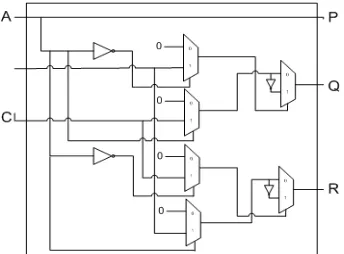
Fredkin Gate with multiplexer (mux) realization
Figure 2:Block diagram of Fredkin gate using mux Output P=A; Q=A’B+AC; R=AB+A’C
MS D Flip Flop Using Basic gates
ISSN (Print) : 2320 – 3765 ISSN (Online): 2278 – 8875
I
nternational
J
ournal of
A
dvanced
R
esearch in
E
lectrical,
E
lectronics and
I
nstrumentation
E
ngineering
(An ISO 3297: 2007 Certified Organization)
Website: www.ijareeie.com
Vol. 6, Issue 12, December 2017
MS Flip Flop using reconfigurable gates
Figure 4:Block diagram of MS FF using reversible gate
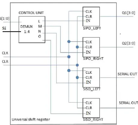
Universal Shift Register 1
Universal shift registers store binary data either it may be zero or one, or when a clock signal is applied it can be shifted left or right. Depend upon the occurrence of the clock input All modes of operation such as serial-in serial-out (SISO), parallel-in parallel-out (PIPO) operation are performed. Figure5 shows the block diagram of universal shift register 1.Figure 5 shows the block diagram of Universal shift register[12].
Figure 5:Block diagram of Universal shift register 1
ISSN (Print) : 2320 – 3765 ISSN (Online): 2278 – 8875
I
nternational
J
ournal of
A
dvanced
R
esearch in
E
lectrical,
E
lectronics and
I
nstrumentation
E
ngineering
(An ISO 3297: 2007 Certified Organization)
Website: www.ijareeie.com
Vol. 6, Issue 12, December 2017
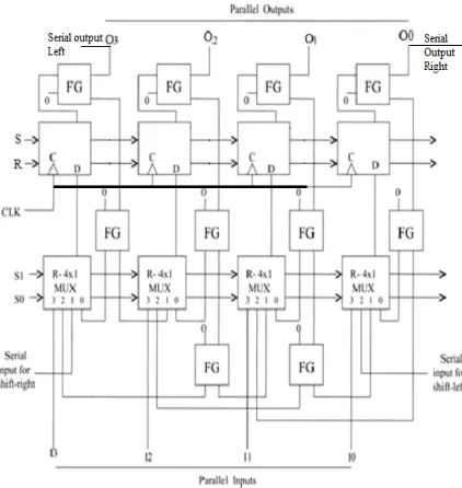
Universal Shift Register 2
The data in the universal shift register can be shifted left or right on the clock signal. The other modes of operation such as serial output left(SOL), serial output right (SOR), parallel output (PO) can also be performed depending upon the select line and occurrence of clock. Block diagram of Universal shift register shown in figure 6.
Figure 6:Block diagram universal shift register
ISSN (Print) : 2320 – 3765 ISSN (Online): 2278 – 8875
I
nternational
J
ournal of
A
dvanced
R
esearch in
E
lectrical,
E
lectronics and
I
nstrumentation
E
ngineering
(An ISO 3297: 2007 Certified Organization)
Website: www.ijareeie.com
Vol. 6, Issue 12, December 2017
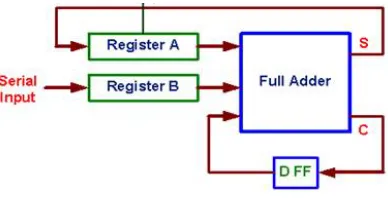
Serial Adder:
We have designed a universal shift register application serial adder shown in Figure 7. that adds two inputs serially and gives the serial output. It consists Serial In Serial Out (SISO) shift register. The block diagram of serial adder consists of two register, one full adder, and d-ff. For SISO shift register we have used the Universal Shift Register 2 with the selection lies to be S1 = 0 and S0 = 1 for making the universal shit register to behave as the SISO right shift register and the input is given to the serial in right. And the output is got from the serial output left. Serial adder is one which has delay less than that of parallel adder.
Figure 8:Block diagram of serial adder
IV.RESULTS
For the experiment considering the proposed Sequential Circuit Elements Using Reversible Logic Gates with MUX, the sequential circuit elements for serial adder using reversible gate with mux is designed using Verilog HDL and synthesized using Xilinx ISE 14.7.The experimental result shows optimal reduction performance of parameters such as Area in terms of LUTs and registers and delay in terms of nano seconds and power.
Parameter Universal shift register reversible
logic dff
Universal shift register reversible
logic -mux
BELS 43 36
Delay
13.710ns 12.576ns
Power
14.68mw 14.59mw
Table 2:Result of universal shift register design 1
Parameter Universal shift register reversible
logic dff
Universal shift register reversible logic mux
BELS 16 12
Delay 16.154ns 15.660ns Power 15.01mw 14.89mw
Table 3: Result of universal shift register design 2
Table 4: Result of serial adder Parameter
Serial Adder reversible logic mux
BELS 28
ISSN (Print) : 2320 – 3765 ISSN (Online): 2278 – 8875
I
nternational
J
ournal of
A
dvanced
R
esearch in
E
lectrical,
E
lectronics and
I
nstrumentation
E
ngineering
(An ISO 3297: 2007 Certified Organization)
Website: www.ijareeie.com
Vol. 6, Issue 12, December 2017
V.CONCLUSION
The Research in the area of Reversible logic is on the prior due to the capability of the reversible logic to lessen the power dissipated which has resulted in loss less circuits. Our proposed sequential circuit element using reversible logic gate with mux realization .the experimental result shows successful reduction in area, delay and power.
VI.FUTURE SCOPE
Sequential circuit element using reversible logic gate with mux realization can be design with using different reversible logic gateand using mux realization and get the improved results, also the proposed design can also be extended to a 8-bit Reversible Universal shift Register.
REFERENCES
[1] Landauer.R “Irreversibility and Heat Generation in the Computational Process”, IBM Journal of Research and Development, 5, pp. 183-191, 1961.
[2] Bennett C H “Logical Reversibility of Computation”, IBM J.Research and Development, pp. 525-532, November 1973. [3] Gordon E. Moore, “Cramming more components onto integrated circuits”, Electronics,Volume 38, number 8, April 19, 1965.
[4] M.Perkowski, L. Joziwak, A. Mixhchenko, A. Al-rabadi, A. Coppola,A. Buller, X. Song, M. Khan, S. Yanushkevich, V. P. Shmerko, and M. Chrzanowska-Jeske. A general decomposition for reversible logic. In Proceedings of the International Workshop on Methods and Representations (RM), 2001.
[5] M.P.Frank, Introduction to reversible computing: motivation, progress ,and challenges. In Proceedings of the 2nd Conference on Computing Frontiers, pages 385–390, 2005.
[6] Fredkin.E and Toffoli T. “Conservative logic,” Int’l.J .Theoretical Physics Vol. 21 pp 219–253. 1982.
[7] Md. Selim Al Mamun, 2Indrani Mandal, 3Md. Hasanuzzaman ,\De-sign of Universal Shift Register Using Reversible Logic IJET Publications UK. All rights reserved September, 2012
[8] H Rohini, S Rajashekar, Priyatam Kumar."Design of basic sequential circuits using reversible logic", 2016 International-l Conferenceon Electrical, Electronics, and OptimizationTechniques (ICEEOT), 2016
[9]G Sree Lakshmi, Dr Kaleem Fatima, B K Madhavi. "Compressor based 8×8 BIT Vedic multiplier using reversible logic", 2016 3rd International
Conference on Devices, Circuitsand Systems (ICDCS), 2016
[10] Feynman.R “Quantum Mechanical Computers,” Optics News, Vol.11, pp. 11–20 1985.
[11] Fredkin.E and Toffoli T. “Conservative logic,” Int’l.JTheoretical Physics Vol. 21 pp 219–253. 1982.