Design of Digital Controller and it’s
Implementation on FPGA for Single Phase
PWM Inverter
Gopal Chaudhari1, Prachi Kale2
Assistant Professor, Dept. of ECE, YTIET, Mumbai, Maharashtra, India1
PG Student, Dept. of EE, YTIET, Mumbai, Maharashtra, India2
ABSTRACT:In this paper the design of control law to calculate width of PWM pulse to generate the desire output voltage is described. Design of hardware and control law is carried out by considering 100 Watt application(load). This design is carried out with state space variable using digital control technique. Digital controlier is design using pole placement technique to achive desire transient response. Also the design of hardware required for single phase PWM inverter is described. The equation for Control law is implemented on FPGA device SPARTAN- III . The parallel processing capability of SPARTAN- III is used to reduce the total time to calculate control law. Also ADC interface circuit ,pulse generating circuit are implemented on FPGA device
KEYWORDS: FPGA ,Digital controller ,single phase ,PWM ,inverter,pole placement technique
I.INTRODUCTION
Inverter is one of important device in power electronics. It convert DC power into variable AC power. Output voltage waveform and frequency can be control by designing controller within inerter system . it is useful for those AC load which require variable AC power. In UPS system ,Inverter play important role. UPS system provide Emergency AC power when utility power system fail. It is require that THD (total harmonic distortion ) in output waveform must be low and transient response of system fast enough[1].
Generally PWM technique is used to control the output voltage of inverter. Width of output pulses is is varied so as to minimize certain harmonics in the output waveform of inverter there are different technique which are used to generate PWM pulses which are used to turn ON and turn OFF switching device of full bridge inverter e.g. i) by comparing triangular waveform with sinusoidal waveform(SPWM) ii) programmed Pwm technique with Microprocessor. These control technique have following disadvantage i) the response time of voltage regulation is usually a few cycle because only average voltage is control ii) the phase difference between reference sine wave and the filter output varied with load. One of well known technique for PWM pattern is deadbeat digital controller. This technique is unique feature of digital control system. Deadbeat means placing all the poles of system of system at origin in Z-domain. In deadbeat control any nonzero error vector will be driven to zero in at most n sampling period if the magnitude scalar.
control U(K) is unbound. Settling time of system depends on sampling period. If sampling time is very small then settling time will also be very small. In deadbeat control ,the sampling period is only the design parameter so if deadbeat response is desire ,designer must choose sampling period carefully so that extremely large control magnitude is not require in normal operation of system the switching device need to handle[7].
The organization of this paper is given as follow i) first section describe general block diagram of system. ii) Second section describes mathematical modeling of system. Iii) Third section describes FPGA implementation of Control system iii) forth section describes the simulated result of control system.
II. SYSTEM DESCRIPTION
.
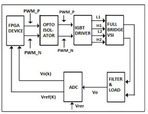
Fig. 1 Block diagram of proposed system
Proposed system is schematically described if fig. 1 full bridge VSI is power unit of system. It is responsible for the conversion of DC power to AC power. Turn ON and turn OFF of various switching device is control by digital controller which is implemented on SPARTAN-III. Width of pulse for +ve Vdc or –Vdc output depend on require voltage by Application(load). This width is calculated by control law. We require sample of output voltage and reference signal for calculation purpose. ADC7891 is used for this purpose. Its working is control by Spartan-III. Digital control law , ADC interface circuit , PWM generating circuit, Arithmetic unit all are synthesized on SPARTAN-III. FPGA device is very dedicate device (low power device) which need to be protected from power section unit (VSI) of system. Optocoupler is used for this work pulse signal from fpga device are applied to optocoupler. Output signal from optocoupler is then connected to gate circuit of IGBT.
III. MATHEMATICAL MODEL OF SYSTEM
VSI unit along with LC filter and load register Rl(plant) is shown in fig. 2
This circuit can be represent by its equivalent circuit as shown in fig 2 output of full bridge VSI circuit is +Vdc or –Vdc which is appliy to LC filter . the equivalent circuit of plant is shown in fig 3. The Gain of this system is given by
= (1)
= §
By solving above equation we will get following equation
̈ = - - 2§ ̇ + ∗ (2)
This is differential equation of VSI system. This equation decides the dynamics of system. If we select Vo and ̇ as a state variable the state equation will be given by
=AX+B (3) Vc = *X (4)
Fig. 3 Equivalent circuit of plant
Where,
X= Vo ̇ , A =−0 −2§1 , B= 0 and =[1 0 ] ;
Equation 3 and 4 represent analog system. if we want its equivalent discrete time system , these equation need to be descritised as follow [7]
X(k+1) =G X(k) + H*U(k) (5)
Y(k) =C X(k) (6)
Where G = =
H = ∫ B
Proposed system can be represented by state space modeling as shown in fig 4.
Now for a given system input reference signal is applied and hence system equation will become as follow
X(k+1) =G X(k) + H*U(k) (7)
Y(k) =C X(k)
And
U (k) =Ko *r (k) –KX (k)
In above equation K matrix is state feedback matrix and Ko is forward gain matrix . K matrix is design to place the available pole of system at desire location in Z-domain. Matrix K is calculated by [7] following equation
K =[ α - α - α - --- α - ]
(8)
Where are coefficient of original system characteristic equation and α are the coefficient of desire characteristic equation
Now transfer function of system describe by equation is given by
F(z) = ( )
( ) = C( − ) *H
Where I is unity matrix and
Characteristic equation of F(z) is given by
|( − )| = + a1 + --- an = 0 (9)
Characteristic equation with state feedback system
|( − + )| = + α + --- α = 0 (10)
And matrix T is given by
Where T = M W ;
M = [ H GH ] ;
W = 1
1 0
Now given system is design for 60Watt load as an example
We will find Rl =
And L ,C component of low pass filter can be found by using equation
Fo = √
In proposed system fundamental frequency (fm) is 50 Hz and switching frequency is 20KHz. Based upon these frequencies, lower order frequency of filter will be 2000Hz [6] Suppose we select high cut-off frequency of low pass filter is 2 kHz then
2000 = √
G = 0.787 45.86∗10
−8.1855∗10 0.7668
H = 0.2
8.3663∗10 ,
M =0.2 0.541
0 −17.852∗10
F(z) = . .
. .
Available pole are
p1 = 0.775 +j0.615 and p2 = 0.775 – j0.615
Characteristic equation of F(z) is given by
|( − )| = - 1.55 z +0.9783
Hence a1 = -1.55 and a2 = 0.9783
Desired pole location
Dp1 = 0.5 +j0.5 and Dp2 = 0.5 – j0.5
Characteristic equation of desired closed loop system
|( − + )| = ( z - 0.5 – j0.5)(z -0.5 +j0.5)
= - z + 0.5 (11)
We find α = -1 and α = 0.5
Matrix K is given by
K =[ α - α - ]
= [ -0.4783 0.55]
We will find matrix K as
K = [0.079 6.0617 *10 ]
Feedback gain matrix K is determined to yield the desired closed loop poles. State feedback through Matrix K changes the characteristic equation for the system, but in doing so the steady state gain of the entire system is changed. Therefore, it is necessary to have an adjustable gain Ko in the system. This gain Ko should be adjusted such that the unit step response of the system at steady state is unity In fig 2.9
U(k) = Ko r(k) –Kx(k)
Then, X(k+1) =(G- HK)x(k) +HKo *r(k)
X(k+1) =G1*X(k) + H1 *r(k) ( )
( ) =G(z) = C(zI – G1) *H1 ( )
( ) =
. .
. . (12)
lim → ( )=lim → (1− ) Y(z) we will find
Derivation of Control law
From fig 5 U(K) is given by,
U (k) =Ko *r (k) –KX (k)
=1.0881*r(k) - 1.079*v(k ) – 6.0617*10 * ( )̇
Now ( )̇ = ( ) ( ) & T = 50µs Hence
U (k) =1.0881 *r (k) -2.291 * ( ) +1.212 ( −1) (13)
Thus pulse width is calculated[7]. This pulse width is require is to control Vc(k) hence I0(K)
IV. FPGA IMPLEMENTATION
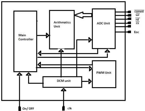
In propose system SPARTAN-III 3s400 is used for the implementation of control law. Block diagram of FPGA
implementation is shown in fig 6 main controller , ADC interfacing unit ,PWM unit , Arithmetic unit are all
implemented on FPGA system
Fig. 6 Block diagram of internal modeling of system in FPGA
V. SOFTWARE DESIGN
Hardware is designed on FPAGA device SPARTAN III (xc 3s 400) to perform following task 1) To get the discrete value of state space variable , ̇ at instant using AD7891
2) To calculate pulse width U (K) using a arithmetic unit 3) Block to generate PWM_P or PWM_N of width U(K)
A MAIN FLOW CHART
VSI. End of ADC start working of arithmetic unit which calculate pulse width. End of arithmetic unit start PWM unit which generate the pwm_p or pwm_n of width given by U (k). End of timer jump to restart cycle.
B. FLOWCHART TO CONTROL AD7891
Flow chart of controller for AD7891 is shown in fig.8. Controller of ADC unit generate the various control signal to control the functionality of AD7891.ADC is set to work in parallel mode. Hardware start conversion is used. In the first step chip enable output is set to logic 1 and control word is written to control resister of AD7891. Control word consist address of current channel and format of converted data (binary or 2s complement). Then start conversion output is set to logic 1. This initiate conversion process. By the end of 1.6 µs EOC(end of conversion)pulse of 90ns will generated by AD7891. After this data is read by setting logic 1 to RD output, Counter is increment by 1 which gives address of next channel for conversion if this data is less than 2 then process will repeat.
Fig.7. Main flow chart of VHDL program
Fig.8 Flowchart to control AD7891 and parallel mode timing diagram
C. FLOWCHART OF PWM UNIT
Fig. 9. Flowchart of PWM unit
VI. SIMULATION RESULT
A. MAIN FLOW CHART WAVEFORM
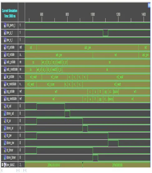
In main controller signal to start the function of ADC section, Arithmetic unit, PWM unit and Timer are generated.
B. ADC UNIT WAVEFORM
+
Fig.11 Control signal generated by ADC block
D PWM Unit Waveform
Fig.13. PWM pulse generated by PWM unit for negative output voltage
VII. CONCLUSION
New approach of real time digital feedback control method which is based on instantaneous control using FPGA (Spartan III) based hardware controller is proposed .A concept FPGA based digital controller is described. control law is design using pole placement technique to achieve desire transient response, total calculation time is approximately using 2MHz crystal freq. which is very less as a result performance of the system improved
REFERENCES
[1] A. Kawamura , T. Hancyoshi :“Deadbeat Controlled PWM Inverter with Parameter Estimation Using Only Voltage Sensor ”IEEEtrans. On PE, Vol.9, No.5,1988
[2] N.Uemura, T. Yokoyama: “Current Control Method Using Voltage Deadbeat Control for Single Phase Utility Interactive Inverter “ INTELEC03,2-2,2003
[3] T. Yokoyama, M. Horiuchi, S.Simigata, “Instantaneous Deadbeat Control for PWM Inverter Using FPGA based Hardware Controller”,IECON 2003
[4] T. Yokoyama, Motoki Horiuchi, Takahiro Fujii, “Comparission of Multirate Deadbeat Control for Single Phase PWM Inverter”IPEC2005 S33-3
[5] Dr. P.S. Bhimra : “ Power Electronics “
[6] Mohan ,Undeland,Robbins : “ Power Electronics “