Substrate Integrated Waveguide without Metallized Wall Posts
Lindo Ouseph*, Anju Mathews, and Aanandan Chandroth
Abstract—A simplified design of substrate integrated waveguide (SIW) is proposed here. The
requirement of side walls using via which is quite cumbersome in the manufacturing process is eliminated in this structure. The design is based on producing an imaginary electric boundary by exciting the SIW using differential feed. It behaves as a pair of half mode substrate integrated waveguides (HMSIWs) sharing a common electric boundary. The new structure gives similar characteristics of the conventional SIW in terms of cutoff frequency, stopband rejection and operating bandwidth.
1. INTRODUCTION
Substrate Integrated Waveguide (SIW) [1] is one of the front runners in emerging planar waveguide technologies for millimeter wave applications. Conceptually, SIW is a dielectric filled rectangular waveguide where metal clad on both sides of the substrate acting as top and bottom walls [2]. The side walls are approximated by periodically placed metal posts. It gives similar performance advantages of a dielectric filled rectangular waveguide such as signal isolation from the surroundings, low loss propagation and small footprint [3]. Several passive devices based on rectangular waveguide and some novel proposals have been implemented in SIW [4–11] in the recent years. Several variations of SIW are introduced to achieve the same level of performance with reduced size and complexity such as half mode SIW (HMSIW) and folded half-mode SIW (FHMSIW) [12, 13]. HMSIW considerably reduces the number of vertical metallizations by exploiting magnetic field symmetry [14]. Many more miniaturization techniques have been proposed with some added complexities [15]. As the operating frequency becomes higher, the dimension of the via holes should be smaller that their fabrication becomes difficult and expensive. This practically limits the application of SIW to frequencies below 100 GHz [16]. The total elimination of via holes will push this barrier to higher frequencies. The quest for total elimination of vertical metallization culminated in the symmetry properties. In this paper, we propose a method to achieve SIW like performance by creating necessary boundary conditions without vertical metal posts.
2. WAVEGUIDE DESIGN
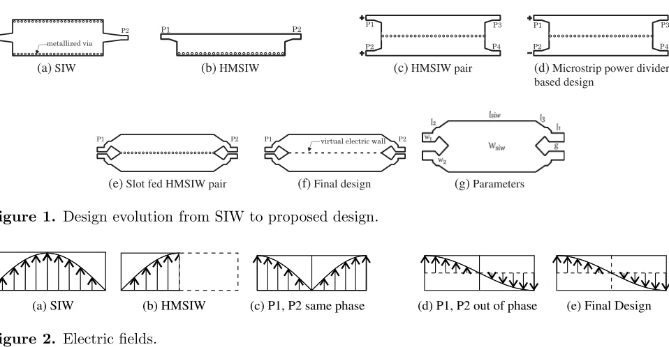
SIW shown in Fig. 1(a) is the planar equivalent of conventional rectangular waveguide. The designs in Fig. 1 have a full ground plane on the other side of the substrate. The side walls are approximated by periodic metal posts. The radius of the via and the space in between them (pitch) should be small enough to provide an effectively continuous and smooth electric boundary. Usually the pitch is set to be much smaller than the guided wavelength and close to the dimension of the metal post. The fundamental mode of propagation in SIW is TE1,0. The electric field distribution is a half wave variation across the
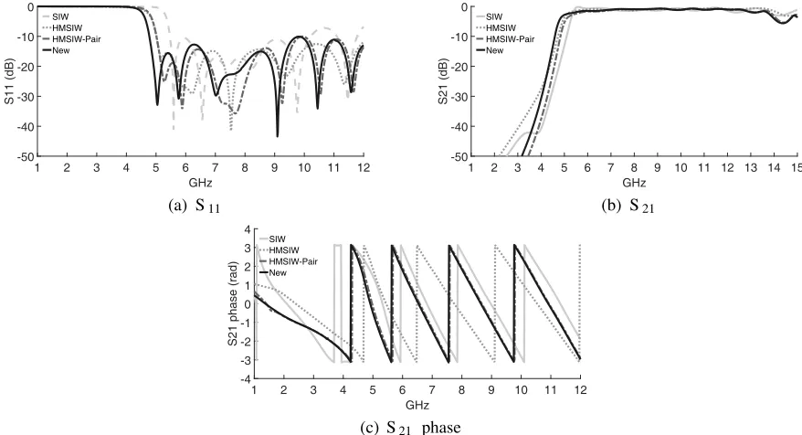
width, shown Fig. 2(a).
Received 18 April 2018, Accepted 29 May 2018, Scheduled 12 June 2018
* Corresponding author: Lindo Ouseph ([email protected]).
(a) SIW (b) HMSIW (c) HMSIW pair (d) Microstrip power divider based design
(e) Slot fed HMSIW pair (f) Final design (g) Parameters
Figure 1. Design evolution from SIW to proposed design.
(a) SIW (b) HMSIW (c) P1, P2 same phase (d) P1, P2 out of phase (e) Final Design
Figure 2. Electric fields.
HMSIW shown in Fig. 1(b) is the next important evolution of SIW. It is assumed that there exists a magnetic boundary at the centre line of the SIW [13]. This symmetry provides sufficient boundary conditions to support a propagation mode, even without half of the structure. The halved width and the reduced number of vias are the advantages of HMSIW. This gives the same properties of the SIW with a slightly different mode of propagation (TE0.5,0). The electric field inside HMSIW is plotted in
Fig. 2(b) which shows a quarter wave variation.
Figure 1(c) shows the HMSIW pair placed side by side such that they share the same electric wall constituted by the metal posts. Both HMSIWs have their feed points marked P1 & P2 as input and P3 & P4 as output. When P1 & P2 are fed in same phase, the electric field for such excitation is shown in Fig. 2(c). The electric field forms a pair of quarter-wave variations and create a mirror image across the centre. There exists a null field at the centre due to the presence of metal posts which act as an electric wall. Another possible mode of excitation is to feed 180◦ out-of-phase signal to P1 & P2 as shown in Fig. 1(d). The electric field distribution in this case is shown in Fig. 2(d). Here the field distribution is skew symmetric with a quarter-wave variation across the centre. Again, the electric field is zero at the centre due the via posts. The design shown in Fig. 1(d) can be fed using a microstrip power divider with unequal path lengths to get 180◦ out-of-phase signals. The specific length results in narrow band operation. To overcome this problem, a coplanar strip (CPS) line to microstrip transition is designed as shown in Fig. 1(e). This consists of three sections. The first part is a CPS line where the electric field is tangential to the substrate plane. The impedance of the CPS line is defined by the slot width (g) and the width of the strip (w1). The second part is a tapered transition from CPS to microstrip line. This is
to rotate the direction of the electric field from horizontal to vertical orientation. The gradual increase in the gap forces the electric field being horizontal to vertical in direction. This is because the tight coupling between the strip becomes weaker, and the interaction with the ground becomes stronger. The width and length of this section are carefully optimised to achieve less reflection. A slight meandering is introduced to make further improvement to theS parameters. The third section is a simple tapering ending with half the width of the waveguide. The length is optimised in simulation. The output of the CPS to microstrip is a differential signal required for the generation of TE0.5,0 mode pair in the
waveguide. The transition makes sure the opposite phase of the signal over much wider frequencies. The parameters used in the optimized design arel1 = 3.8 mm, l2 = 3.6 mm,l3 = 5.4 mm,lsiw = 50 mm,
g= 0.04 mm,w1 = 2.4 mm,w2 = 3.6 mm andwsiw = 20 mm. Even after the removal of metal posts, the
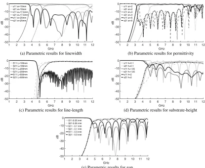
The numerical simulations are carried out using solvers in CST Studio Suite. All the simulation results reported in this paper are done using frequency domain solver which is based on finite element method with higher order tetrahedral mesh. Open boundaries are assigned for all the sides except the ground plane which is set as perfect electric boundary. Simulation results are validated using transient solver which is based on finite integral technique with hexahedral mesh, keeping adaptive refinement enabled with extended maximum solver duration. Rogers RT5880 (r = 2.2, Thickness = 0.79 mm) with loss (tanδ = 0.0009) is chosen as substrate. Perfect electric conductor is assigned for all the conducting regions.
The cutoff frequencies of all the designs are fixed around 4.7 GHz. A small decrease in cutoff frequency of open structures are due to the fringing fields which contribute to the increased effective electric width of the waveguide section. The phase ofS21 for all the structures are plotted in Fig. 3(c).
For all the four designs, the linearity of phase is preserved throughout the operating band. In the passbandS21stays above −1 dB, and S11stays below −10 dB. For all the topologies, similar results are
observed.
1 2 3 4 5 6 7 8 9 10 11 12
GHz -50
-40 -30 -20 -10 0
S11 (dB)
SIW HMSIW HMSIW-Pair New
(a) S11
1 2 3 4 5 6 7 8 9 10 11 12 13 14 15
GHz -50
-40 -30 -20 -10 0
S21 (dB)
SIW HMSIW HMSIW-Pair New
(b) S21
1 2 3 4 5 6 7 8 9 10 11 12
GHz -4
-3 -2 -1 0 1 2 3 4
S21 phase (rad)
SIW HMSIW HMSIW-Pair New
(c) S21 phase
Figure 3. Simulation results for different structures in evolution.
The simulated fields at 8 GHz inside the entire structure are shown in Fig. 4. Electric fields at three sections of the transition are shown in Fig. 4(a). In the CPS region the electric field is strong between the strips and observed a relatively small interaction with the ground plane. This behaviour starts to change when the gap diverges. The vertical field becomes strong, and the horizontal field becomes much weaker. The structure of transverse electric field is similar to the field plotted in Fig. 2(e) with the maxima at the open edges of each section. The presence of electric null is clearly visible throughout the length of the waveguide. This verifies the existence of electric wall that is essential for the operation.
The magnetic field is shown in Fig. 4(b). The presence of symmetric half circles in the waveguide region is as expected. The magnetic fields at the open faces are normal to the side of the waveguide. This is similar to the behaviour of magnetic wall. From both electric and magnetic fields, it is evident that sufficient boundary conditions exist in the design to support the propagation mode (TE0.5,0). So
with this proposal, the requirement of via from SIW is completely eliminated.
(a) Electric field
(b) Magnetic field
Figure 4. Simulated field distributions inside the proposed waveguide at 8 GHz.
1 2 3 4 5 6 7 8 9 10 11 12
GHz -50 -40 -30 -20 -10 0 dB s11 w=10mm s21 w=10mm s11 w=17.5mm s21 w=17.5mm s11 w=25mm s21 w=25mm
(a) Parametric results for linewidth
1 2 3 4 5 6 7 8 9 10 11 12
GHz -50 -40 -30 -20 -10 0 dB s11 er=2 s21 er=2 s11 er=4 s21 er=4 s11 er=5 s21 er=5
(b) Parametric results for permittivity
1 2 3 4 5 6 7 8 9 10 11 12
GHz -50 -40 -30 -20 -10 0 dB S11 L=100mm S21 L=100mm S11 L=200mm S21 L=200mm S11 L=500mm S21 L=500mm
(c) Parametric results for line-length
1 2 3 4 5 6 7 8 9 10 11 12
GHz -50 -40 -30 -20 -10 0 dB s11 h=0.1 s21 h=0.1 s11 h=1.05 s21 h=1.05 s11 h=2 s21 h=2
(d) Parametric results for substrate-height
1 2 3 4 5 6 7 8 9 10 11 12
GHz -50 -40 -30 -20 -10 0 dB S11-0.05 mm S21-0.05 mm S11 - 0.1 mm S21 - 0.1 mm S11 - 0.3 mm S21 - 0.3 mm
(e) Parametric results for gap
also verified with simulation, and results are plotted in Fig. 5(b). The frequency shifts are in agreement with the SIW model.
The effect of length of the waveguide is also studied and shown in Fig. 5(c). It proves that the responses are not much affected by the length. Since the loss in the substrate used is very small, the length also does not contribute any serious dielectric losses in the waveguide.
In rectangular waveguide, the conductive losses are related to the waveguide height. The responses of the waveguide for different heights are plotted in Fig. 5(d). Since the response includes the effects from the transition, it is difficult to differentiate the effect of height alone. However, when the height becomes too small, the performance becomes poor. This is also true for larger heights, where operation band shrinks from the optimum.
The matching of slot line is sensitive to the gap width. This is parametrically studied in Fig. 5(e). As the gap width deviates from the optimum value to either side, the reflection starts to increase and reaches a point where the transition becomes ineffective. So careful fabrication is needed for desired performance.
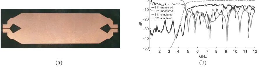
A photograph of fabricated structure is shown in Fig. 6(a). The structure is probed using a pair of wideband microstrip to coplanar slot transition [17] structures connected at the ends of the device. The measurements are taken using Rhode & Schwartz ZVB20 vector network analyser. The measured scattering parameters for the final design are plotted in Fig. 6(b) along with the simulated results. The cutoff frequency and bandwidth match with the simulation. The deteriorated performance may be due to parasitic effects and losses at the probe contact. With better fabrication and probing technique, this drawbacks may be mitigated.
(a) (b)
GHz -50
-40 -30 -20 -10 0
dB
1 2 3 4 5 6 7 8 9 10 11 12
Figure 6. (a) Photograph of fabricated structure. (b) Comparison of measured results with simulation.
4. CONCLUSION
A new SIW concept without physical metallic walls is proposed. A CPS to 180◦out of phase differential microstrip feed is designed to excite TE0.5,0 mode pair in the waveguide. The proposed and simulated
electric and magnetic fields match perfectly. The simulation and measurements of the scattering parameters also agree well. The performance of the proposed waveguide is proven similar to that of rectangular waveguide, SIW and HMSIW. Parametric studies are conducted to study the effect of key variables in the performance of the waveguide. The proposed design is less complex, cost effective and can be used for much higher frequencies than that possible with SIW.
ACKNOWLEDGMENT
REFERENCES
1. Wu, K., D. Deslandes, and Y. Cassivi, “The substrate integrated circuits — A new concept for high-frequency electronics and optoelectronics,”6th International Conference on Telecommunications in Modern Satellite, Cable and Broadcasting Service, Vol. 1, P-III-P-X, October 2003.
2. Che, W., K. Deng, D. Wang, and Y. L. Chow, “Analytical equivalence between substrate-integrated waveguide and rectangular waveguide,” IET Microw. Antennas Propag., Vol. 2, No. 1, 35–41, February 2008.
3. Deslandes, D. and K. Wu, “Accurate modeling, wave mechanisms, and design considerations of a substrate integrated waveguide,” IEEE Trans. Microw. Theory Tech., Vol. 54, No. 6, 2516–2526, 2006.
4. Cai, Y., Y. Zhang, Z. Qian, W. Cao, and S. Shi, “Compact wideband dual circularly polarized substrate integrated waveguide horn antenna,” IEEE Transactions on Antennas and Propagation, Vol. 64, No. 7, 3184–3189, July 2016.
5. Parment, F., A. Ghiotto, T. P. Vuong, J. M. Duchamp, and K. Wu, “Low-loss air-filled substrate integrated waveguide (SIW) band-pass filter with inductive posts,”European Microwave Conference (EuMC), 761–764, 2015.
6. Doghri, A., T. Djerafi, A. Ghiotto, and K. Wu, “Substrate integrated waveguide directional couplers for compact three-dimensional integrated circuits,” IEEE Trans. Microw. Theory Tech., Vol. 63, No. 1, 209–221, January 2015.
7. Cheng, Y. J., “Substrate integrated waveguide frequency-agile slot antenna and its multibeam appication,” Progress In Electromagnetic Research, Vol. 130, 153–168, 2012.
8. Huang, Y., Z. Shao, and L. Liu, “A substrate integrated waveguide bandpass filter using novel defected ground structure shape,”Progress In Electromagnetic Research, Vol. 135, 201–213, 2013. 9. Huang, J.-Q., D. Lei, C. Jiang, Z. Tang, F. Qiu, M. Yao, and Q.-X. Chu, “Novel circularly polarized SIW cavity-backed antenna with wide CP beamwidth by using dual orthogonal slot split rings,” Progress In Electromagnetic Research C, Vol. 73, 97–104, 2017.
10. Moro, R., S. Agneessens, H. Rogier, A. Dierck, and M. Bozzi, “Textile microwave components in substrate integrated waveguide technology,” IEEE Trans. Microw. Theory Tech., Vol. 63, No. 2, 422–432, February 2015.
11. Parment, F., A. Ghiotto, T. P. Vuong, J. M. Duchamp, and K. Wu, “Air-filled substrate integrated waveguide for low-loss and high power-handling millimeter-wave substrate integrated circuits,” IEEE Trans. Microw. Theory Tech., Vol. 63, No. 4, 1228–1238, April 2015.
12. Grigoropoulos, N., B. S. Izquierdo, and P. R. Young, “Substrate integrated folded waveguides (SIFW) and filters,” IEEE Microw. Wirel. Compon. Lett., Vol. 15, 829–831, 2005.
13. Hong, W., B. Liu, Y. Q. Wang, et al., “Half Mode substrate integrated waveguide: A new guided wave structure for microwave and millimeter wave application,”Proc. Joint 31th Int. Conf. Infrared and Millimeter Waves/14th Int. Conf. Terahertz Electronics Shanghai, 18–23, September 2006. 14. Lai, Q., Ch. Fumeaux, W. Hong, and R. Vahldieck, “Characterization of the propagation properties
of the half-mode substrate integrated waveguide,” IEEE Trans. Microw. Theory Tech., Vol. 57, 1996–2004, 2009.
15. Wang, N., C. Jin, X. Xu, and H. Sun, “Quarter-mode substrate integrated waveguide,”Asia-Pacific Microwave Conference, Sendai, Japan, 286–288, 2014.
16. Bozzi, M., A. Georgiadis, and K. Wu, “Review of substrate-integrated waveguide circuits and antennas,”IET Microwaves, Antennas & Propagation, Vol. 5, No. 8, 909, 2011.