3T Gain Cell EDRAM for Low Power
Application
*A.CHANDANA **MR.B.SATEESH ***MR .G.BABU
*M.TECH Dept of ECE,VAAGDEVI COLLEGE OF ENGINEERING
**Assoc. prof Dept of ECE, VAAGDEVI COLLEGE OF ENGINEERING
***Assoc. prof Dept of ECE, VAAGDEVI COLLEGE OF ENGINEERING
Abstract
—
Logic compatible gain cell (GC)-embedded
DRAM (eDRAM) arrays are considered an
alternative to SRAM because of their small
size, non rationed operation, low static
leakage, and two-port functionality. But
traditional GC-eDRAM implementations
require boosted control signals in order to
write full voltage levels to the cell to reduce
the refresh rate and shorten access times.
The boosted levels require an extra power
supply or on-chip charge pumps, as well as
nontrivial level shifting and toleration of
high voltage levels. In this paper, we present
a novel, logic compatible, 3T GC-eDRAM
bit cell that operates with a single-supply
voltage and provides superior write
capability to the conventional GC structures.
The proposed circuit is demonstrated in
0.25μm CMOS process targeted at low
power, energy efficient application.
I. INTRODUCTION
Memories have occupied large proportion of
the die area of VLSI system-on chips in
recent years. Major reason for this is
increasing number of components as in case
of 6T SRAM it has large 6-transistor the
various other reasons are area-consuming,
peripheral circuitry. Embedded memories
have turned to be an important one in the
long standby mode it continues to leak more
power which characterize the system
Initially SRSAMs are used for storing
data bits in memory. But it has some of the
disadvantages like large area, more power
consumption even though it has been the
traditional choice for the implementation of
embedded memories due to its high-access
speed and refresh-free data retention time. It
also have some other disadvantages like
static leakage of current, under voltage
scaling and large transistor count. These
limitations can be overcome by usage of
gain-cell (GC)-embedded DRAM (eDRAM)
such as circuit in Fig. 2 and Fig. 3 [3]-[8].
Which provides full CMOS logic
compatibility of transistor (2T) or
2-transistor (3T) GC-eDRAMS resulting in
nonratioed operation and low static leakage
currents from VDD to GND. Inspite of
overcoming most of the disadvantages of
static memories GC-eDRAM requires
periodic refreshing operation. However, as
opposed to static memories the data
retention time of GC-eDRAM depend on
dynamically stored charge.
II. EXISTING METHOD
A. 6T SRAM
Basic static RAM circuits can be viewed as
vibrations on the designs used for latches
and flip-flops more aggressive static RAMs
make use of design tricks originally
developed RAMs to speed up the system.
The value is stored in the middle four
transistors, of Fig.1 which form a pair on
inverters connected in a loop. The other two
transistors control access to the memory cell
by the bit lines. When select = 0, the
inverters reinforce each other to store the
value. A read or write is performed when
To read, bit and bit are precharged to before
the select line is allowed to go high. One of
the cell’s inverters will have its output at 1,
and the other at 0, which inverter is 1
depends on the value stored. The right hand
inverter’s pull down and the bit line will be drained to through that inverter’s pull down
and the bit line will remain high. If the
opposite value is stored in the cell, the bit
lines will be pulled own while bit remains
high.
To write, the bit and bit lines are set to the
desired value, then select is set to 1.charge
sharing forces the inverters to switch values,
if necessary, to store the desired value. The
bit lines have much higher capacitance than
the inverters, so the charge on the bit lines is
enough to overwhelm the inverter pair and
cause it to flip state.
B. 2T Mixed Gain Cell
2T mixed GC can be implemented with
either an NMOS or a PMOS device as
shown in Fig.2. Moreover, both MW (write
transistor) and MR (read transistor) can be
implemented with standard threshold
voltage core or high threshold voltage I/O
devices in the considered CMOS
technology. Due to the voltage drop across
MW, a boosted write word line
(WWL)voltage is required during write
access above for NMOS operation and
below for PMOS operation.
For a read operation a PMOS MR requires a
pre-discharge of the parasitic RBL
capacitance followed by raising the read
word line (RWL). If the selected bitcell’s
storage mode (SN) holds a loop value,MR is
conducting and charges RBL post a
detectable sensing threshold. If SN holds
value MR is cut-off such that RBL remains
discharged below the sensing threshold. For
operation is exactly opposite i.e. RBL is
precharged and RWL is lowered to initiate a
read.
III.
PROPOSED METHOD
In this brief, we present a new topology for a
3TGC, featuring a complementary
transmission gate in the write port. While
the proposed solution is quite straight
forward it is novel and its impact in very
high. We demonstrate the functionality of
the proposed system used in ultra-low power
applications such as biomedical sensor
nodes and implants. The proposed 3T
GC-eDRAM macro is shown to be fully
functional with a supply voltage ranging
from 600mv to 2.5v.
A. 3T Gain Cell eDRAM
3T GC consists of write port featuring a
complementary transmission gate PMOS
write (PW) and NMOS write (NW) a
storage node (SN) composed of the three
transistors, a read port based on NMOS read
(NR) and the metal interconnect as in Fig 3.
the GC is built that all the transistors
operates with standard voltage and is fully
compatible with standard digital CMOS
technologies. The gates of PW and NW are
connected to the world line of PMOS and
NMOS WWLp and WWLn. A common
write bit line is used to drive the data to the
transmission gate during write operations.
When the full-swing is given to the cells
transmission gate enables the propagation of
strong levels to the SN without any need for
boosted world line.
Read operation is performed by precharging
the read bit line (RBL) to and subsequently
driving the read word line (RWL) to GND.
If the storage node is already high it
discharges RBL capacitances or blocking
the discharge path if SN is low. IN order to
achieve a tradeoff between speed, area,
amplifier can be used to improve the read
operation and its performance as described
in [5],[6].
B. Operation
The circuit is described with = 900 mv. This
voltage was chosen as a good medium
voltage between and since the data retention
time (DRT) is proved to be efficient in.
GC-eDRAM design [8] at this voltage starting
with charged WBL is driven low and the
world lines WWLp is set to 0 and WWLn is
set to . Then a strong 0 level is passed to the
SN, during standby, the level on SN
deteriorates due to leakage currents
dominated by the sub threshold leakage of
PW and NW in mature CMOS nodes. Hence
in order to extend the retention time WBL is
driven to during standby and read cycles
thereby significantly reducing the sub
threshold leakage through the transmission
gate for both stored low and high values
compared with the condition where WBL is
either driven to either or GND. The write
circuitry and read circuitry are described in
section IV.A. During readout the 0 level
blocks the discharge paththrough NR,
maintaining the precharged voltage on RBL.
During the next write operation WBL is
driven high, resulting in a strong 1 stored on
the SN. The subsequent read operation
provides a strong gate overdrive to transistor
NR, thereby discharging RBL toread a 1. It
should be noted that during this operation
(Read 1), bitcells storing 1 and sharing
thesame column turn on when RBL
discharges by more than the of NR, causing
it to saturate before it can completely
discharge. This phenomenon is common to
many GC-eDRAM configurations, as
discussed in[8].
C. Data Retention Time
The data retention time (DRT) of GC
embedded DRAMS is the time interval for
writing a data level in the bit cell to the last
moment the data can still correctly read out
the stored information. For 2T and 3T cells
methodology which are affected by the
initially degraded voltage level
corresponding to the data values due to the
threshold voltage () drop across the write
transistor DRT is primarily limited by the
initial charge stored on the internal bit cell
capacitance and the leakage currents that
degrade the stored voltage level over time. In
order to describe this issue a boosted write
world line (WWL) voltage is usually employed to
pass a full swing level to the storage
capacitance. Any how this requires the
generation of boosted on-chip voltage, which
of the voltage boost is set not only to overcome
the drop, but also to achieve short write access
time which otherwise are typically longer than
6T SRAM implementation. The proposed bitcells
provides strong initial data levels for enhanced
DRT and robust operation as well as for fast
write access time.
IV. MEMORY
MACRO PERIPHERALS
To improve the array performance in terms
of access time and power consumption
several peripheral techniques were
integrated into the designed memory macro
in the proposed technique single supply
voltage is provided to the circuit which
simplifies the implementation of a full
memory macro. This is the significant
advantage over the other GC eDRAMS that
uses conventional bit cells. These bit cells
require the use of level shifters to create the
desired boosted or negative voltage supply
depending on the types of MOS write. The
peripheral circuit which is designed for this
memory macro and their techniques are
described as follows.
A. Readout Circuitry
Large number of ultra low power systems
comprising of low voltage embedded
memories consists of simple sense inverter.
This sense inverter is used for the purpose of
reduction in area, robust and low power
readout operation however this inverter
suffers from very slow data readout as it
requires RBL to be discharged or charged
for PMOS read device switching the
threshold of the inverter.
This operation is further impeded
by the before mentioned. In order to
overcome this limitation the readout path
that was integrated into the proposed 3T
GC-eDRAM macro cell has two sensing
node 1). A faster dynamic sensing mode but
it is potentially more error-phrone which
slower static mode but more reliable. In both
the sensing modes however threshold device
PMOS transistors were used in order to
allow a faster read access time due to the
above mentioned problem the read out
circuitry is provided the supply voltage
through the read enable signal in order to
save substantial static power because of the
leaky low voltage threshold devices the
schematic diagram with the two sensing nodes
of static and dynamic are shown in Fig. 4.RBL
saturation during readout that slows down the
charging and discharging operation as the RBL
voltage increases and decreases The raising
edge of the read clock (RCLK) creates a
precharge pulse that charges the parasitic
capacitance of RBL and discharges the dynamic
sense inverter output capacitance through the
discharge transistor, . Subsequently RBL is
conditionally discharge during read operation
turning on to complement the output if high
value is stored in the selected cell. Therefore an
RBL swing of only one threshold voltage is
required to complete a read operation.
B. Write Circuitry
The proposed single supply 3T bit cell
provide a significant improvement in write
time when compared to the read time, which
means it has fast access time, when
compared to the readout circuitry. It also has
an initial SN level improvement over
standard GC implementation the dual
transistor write port built by means of
transmission gate provides a leakage path to
or from the storage node. The write circuitry
to implement the median WBL bias during
standby and read cycle is shown in Fig.5.
The increased aggregated sub-
current causes faster degradation of the
stored charge, leading to reduced DRT, as
compared with a reference 2T cell. In
addition, several previous works have shown
that the data dependent, asymmetric DRT
(for data 0 and 1) of standard GCs can be
biasing the WBL at the best case voltage for
the weaker data level during standby and
read operations . For the proposed 3T
configuration, the worst case DRTs of the 1
and 0 levels are similar, and significant
deterioration of the stored levels occurs for
both extreme values of WBL bias (VDD and
GND).
A standard inverter chain conditionally
drives the data-in level on to the WBL
through a TG, controlled by complementary
write enable signals Write Enable (WE) and
Write Enable Negative (WEN). In parallel, a
pair of long-channel I/O devices drives
WBL during non-write cycles. These
devices create a short-circuit path between
VDD and GND when WE is low, providing
a median potential (VDD/2) at WBL. Due to
the thick oxides and long channel-lengths of
the I/O devices, process variations are
significantly reduced, and the static current
is extremely low compared to the readout
circuit.
V.
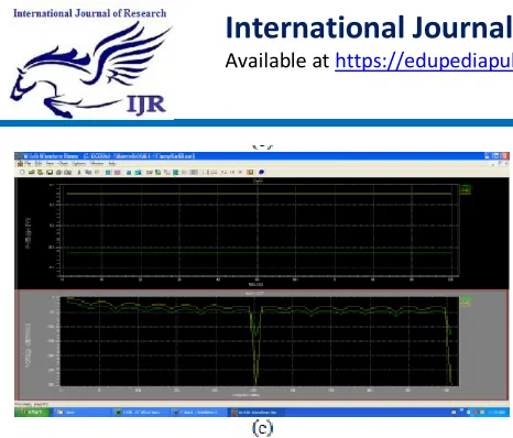
RESULTS AND DISCUSSIONS
The functionality of the memories at
different frequencies for various voltage
range are shown in Fig. 7 and their
corresponding power consumptions results
follows. The main aim of the proposed
techniques is that 3T GC-eDRAM should
consume less power than that of the other
memories such as static RAM (SRAM)
designed with 6 transistors and 2T mixed
GC DRAM architecture 3T GC-eDRAM has
a average power consumption of 12.71μW
which is less when compared to other
existing memories 6T SRAM and 2Tmixed
GC which consumes average power of
36.85μW and 13.2μW respectively. The
result shows that the proposed technology
consumes very less power than that of static
memory. For a dynamic memory relevant
metric for static power consumption is
retention power, composed of the sum of
leakage and refresh power. Hence it is
essential to be much more low so that the
power consumption due to leakage and
refreshing operation get reduced. The data
retention power of 3T GC-eDRAM is
4.66nW where for the 2T mixed GC is
5.98nW. It shows that proposed technique
has less leakage power and power required
for refresh than 2T mixed GC as shown in
TABLE 1. The memory frequency is limited
by the read access time during readout, RBL
needs to discharge in order to flip the sense
inverter the operation strongly depends on
the parasitic capacitance of RBL. Hence it
consumes more power than the write
architecture. The readout circuit consumes
an average power of 35.11μW and write
circuitry consumes an average power of
18.49μW. Hence naturally readout circuit
has more read access time than that of the
write access time of write circuitry. The read
access time is 2.1ns whereas the write access
time is 1.8ns respectively.
POWER
VI. FUTURE WORK
This brief proposes a novel 3T GC eDRAM
microcell targeted at ULP systems and
providing high storage density. The
proposed GC is operated from a
single-supply voltage, eliminating the need for
boosted voltages, commonly found in
prior-art implementations. When compared with
6T SRAM technology and 2T mixed gain
cell technology it has less consumption of
power and becomes fully functional at the
voltage range of 600mv to 2.5v showing a
worst case Data Retention power of 4.6 nW
at 900mv.The proposed cell exhibits faster
write-access than conventional GC circuits,
thereby increasing DRTs and reducing
refresh power consumption. The average
power consumption at write access time is
less than that of read access time.
Measurement resultsshow full functionality
at voltages ranging from 600 mv to 2.5 V
with power as much as lower than a
previously reported 6T SRAM in the same
technology node. Testing is the major issue
in eDRAM technology. So in future various
testing method can be used to check the
better performance of the circuit.
VII.CONCLUSION
This brief proposes a novel 3T GC eDRAM
microcell targeted at ULP systems and
providing high storage density. The
proposed GC is operated from a
single-supply voltage, eliminating the need for
boosted voltages, commonly found in
prior-art implementations. When compared with
6T SRAM technology and 2T mixed gain
cell technology it has less consumption of
power and becomes fully functional at the
voltage range of 600mv to 2.5v showing a
worst case Data Retention power of 4.6 nW
at 900mv.The proposed cell exhibits faster
write-access than conventional GC circuits,
thereby increasing DRTs and reducing
power consumption at write access time is
less than that of read access time.
Measurement results show full functionality
at voltages ranging from 600 mv to 2.5 V
with power as much as lower than a
previously reported 6T SRAM in the same
technology node. Testing is the major issue
in eDRAM technology. So in future various
testing method can be used to check the
better performance of the circuit.
REFERENCES
[1] Raychowdhuryet al., “PVT-and-aging
adaptive word line boosting For 8T SRAM
power reduction,” in Proc. IEEE ISSCC,
Feb. 2010, pp. 352353.
[2] A. Teman, P. Meinerzhagen, R.
Giterman, A. Fish, and A. Burg, “Replica
Technique for adaptive refresh timing of
gain-cell-embedded DRAM,”IEEE Trans.
Circuits Syst. II, Exp. Briefs, vol. 61, no. 4,
pp. 259–263, Apr2014
[3] D. Somasekharet al., “2 GHz 2 Mb 2T
gain cell memory macro with 128
GBytes/sec bandwidth in a 65 nm logic
process technology,”IEEE J. Solid-State
Circuits, vol. 44, no. 1, pp. 174–185, Jan.
2009.
[4] G. M. S. Reddy and P. C. Reddy,
“Design and implementation of 8k-bits Low
power SRAM in 180nm technology,” in
Proc. IMCECS, vol. 2. 2009,
[5] K. C. Chun, P. Jain, T.-H. Kim, and C.
H. Kim, “A 667 MHz logic compatible
embedded DRAM featuring an asymmetric
2T gain cell for high speed on-die caches,”
IEEE J. Solid-State Circuits, vol. 47, no. 2
pp. 547–559, Feb. 2012.
[6] K. C. Chun, P. Jain, J. H. Lee, and C. H.
Kim, “A 3T gain cell embedded DRAM
utilizing preferential boosting for high
density and low power on die Caches,”
IEEE J. Solid-State Circuits, vol. 46, no. 6,
pp. 1495–1505, Jun. 2011.
[7] K. C. Chun, W. Zhang, P. Jain, and C. H.
Kim, “A 2T1C embedded DRAM macro
with no boosted supplies featuring a 7T
SRAM based Repair and a cell storage
monitor,” IEEE J. Solid-State Circuits, vol.
47,no. 10, pp. 2517–2526, Oct. 2012.
AUTHOR1:-
*A.CHANDANA completed
her B.Tech in VAAGDEVI
ENGINEERING COLLEGE in 2014 and
M.Tech completed in VAAGDEVI
COLLEGE OF ENGINEERING
**MR.B.SATEESH working
as Assoc. prof in Dept of ECE, VAAGDEVI
COLLEGE OF ENGINEERING
AUTHOR3:-
*** MR.G.BABU working as Assoc. prof in
Dept of ECE, VAAGDEVI COLLEGE OF