Performance analysis of
Modified SRAM Memory Design using leakage
power reduction
1
Udaya Bhaskar Pragada ,2J.S.S. Ra ma Ra ju, 3Mahesh Gudivaka 1
PG Student,2Associate Professor, 3Assistant Professor 1
Electonics and Co mmunication Engineering, 1
Bhimavara m Institute of Engineering and Technology , Andhra Pradesh,India
_________________________________________________________________________________________ _______________ Abstract—The present worl d aims in designing low power de vices due to the r ampant usage of por table battery powere d g adgets. The pr oposed static r andom access memor y (S RAM) design furnishes an appr oach towar ds curtailing the hol d power dissipati on. The design uses a tail transistor which ai ds in li miting the shor t circuit power dissipation by disrupting the direct connecti on between supply voltage and ground. This tail tr ansistor also brings down the subthreshol d current by provi ding stacking effect, which subse que ntl y re duces hol d power dissipati on. A suppl y voltage of 0.8V is used which makes it eligible for low power applications. The designe d SRAM cell has single ende d write and re ad oper ations and is simulate d using TANNER EDA 45nm CMOS technolog y. The pr opose d SRAM cell has a low power consumptionwhich is much less as compare d to the standar d 6T S RAM cell.
Keywords—power consumption, hold power dissipation, SRAM, stacking effect, subthreshold current
IndexTerms— Tanner EDA using S- Edit.
________________________________________________________________________________________________________
I. IN TRO DUC TION
Now a day‘s to reduce the silicon area and to achieve high speed and performance, the devices are being scaled down to a grea t extent. Generally supply voltage is scaled down to reduce the static power dissipation, but along with that for high performance the threshold voltage should also be scaled down. The reduction in the threshold voltage exponentially increases the sub threshol d leakage current which leads to increment in the static power dissipation. Static power dissipation is mainly contributed by sub threshold current and gate leakage current. The cache memory in a microprocessor occupies more than 50% of chip area so the leakage power of cache is a major source of power dissipation in the processor. The total leakage power in SRAM cell is determined by the contribution of leakage currents in each transistor of SRAM cell. The leakage current has two main sources, sub-threshold leakage current and gate leakage current (leakage current is dominated by sub -sub-threshold leakage).
The growing demand of portable battery operated systems has made energy efficient processors a necessity. For applications like wearable co mputing energy efficiency takes top most priority. These embedded systems need repeated charging of their batteries. The problem is more severe in the wireless sensor networks which are deployed for monitoring the environmental parameters. These systems may not have access for recharging of batteries. We know that on chip me mories determine the power dissipation of SoC chips. Hence it is very important to have low power and energy efficient and stable SRAM which is ma inly u sed for on chip me mories. There are various approaches that are adopted to reduce power dissipation, like design of circuits with power supply voltage scaling, power gating and drowsy method. Lower power supply voltage reduces the dynamic power in quadratic fashion and leakage power in exponential way. But po wer supply voltage scaling results in reduced noise margin. Many SRAM arrays are based on minimizing the active capacitance and reducing the swing voltage. In sub -100n m region leakage currents are ma inly due to gate leakage and sub threshold leakage curren t. High dielectric constant gate technology decreases the gate leakage current. Forward body biasing methods and dual Vt techniques are used to reduce sub threshold leakage current. In sub thresho ld SRAMs power supply voltage (VDD) is lower than the transistor threshold voltage (Vt) and the sub threshold leakage current is the operating current.
This project we are analyzing the power consumption of SRAM cell and we are divided into three parts of this project. They are 1. Basic 6T SRAM me mory cell
2. Proposed 6T SRAM cell
3. 6T SRAM using MTCMOS Technique
Figure 1: Conventional 6T SRAM cell
The conventional SRAM (6T) cell has been found to be rather unstable for deep nano -scale technology. This cell fails to meet the so many operational requirements due to the low read static noise margin (SNM). So many configurations have been proposed for improving the stability (SNM).
One way to reduce the power of an SRAM is to reduce the supply voltage (VDD). The way investigated in this brief is to reduce the device size to the nanometer region. Reducing the device size by one-half cuts the gate capacitance by one-fourth, which should result in a large reduction in power consumption. However, if we try to use a nano scale SRAM in a system, we fi nd that the static noise margin (SNM) is too small due to the larg e variation in threshold voltage (VT). So, we have to develop a new SRAM circuit. Our previous study of SNM showed that an SRAM with a single bit line (BL) had a larger SNM than one with two BLs, and that the BL precharge voltage should be lower than VDD.
Read Operation: When M3, M4 is turned on the voltage level of colu mn BLB will not show any significant variation since no current will flo w through M4 and M1 and M3 will conduct a nonzero current and the voltage level of colu mn BL will begin to dr op slightly and the voltage V1 will increases from its initia l value of 0V, where V1 is the voltage across node 1. If W/ L ratio of acc e ss transistor M3 is large compared to the ratio of M1, the node voltage V1 may e xceed the threshold voltage of M2 during this process, forcing an unintended change of the stored state.
Write Operation: Now consider the write "0" operation, assuming that logic "1" is stored in the SRAM cell initially. Figure 2.3 shows the voltage levels in the CMOS SRAM cell at the beginning of the data-write operation. The transistors M1 and M6 are turned off, while the transistors M2 and M5 operate in the linear mode. Thus, the internal node voltages are V1 = VDD and V2 = 0 V before the cell access (or pass) transistors M3 and M4 are turned on.
The column voltage VC is forced to logic "0" level by the data -write circuitry; thus, we may assume that VC is approximate ly equal to 0 V. Once the pass transistors M3 and M4 are turned on by the row selection circuitry, we expect that the node voltage V2 re mains below the threshold voltage of Ml, since M2 and M4 are designed according to condition.
Consequently, the voltage level at node (2) would not be sufficient to turn on Ml. To change the stored information, i.e., to force V1, to 0 V and V2 to VDD, the node voltage V1, must be reduced below the threshold voltage of M2, so that M2 turns off first. When V = VT, the transistor M3 operates in the linear region wh ile M 5 operates in saturation.
III. PRO POSED METHO D
Fig 2. Modified 6T SRAM me mo ry cell
The working of the proposed cell can be div ided into three parts namely hold, read and write operations. These operations are expla ined as follows:
Hold Operation: For hold state, read and wrt are kept low. If n_1 is holding ‗0‘, then NM0 would be off and PM1 would be o and hence n_2 will be connected to logic high. This in turn would turn off PM0 wh ich cuts off n_1 fro m VDD, hence a zero is ma intained at n_1. Simila r is the case for holding ‗1‘.
Read Operation: In the standard operation, bit lines are precharged and then the read is given high. During the read operation, the internal voltage of node storing zero rises which may result in flipping off contents of th e cell. Hence data gets corrupted. In the proposed structure this case is not possible. Apart from this, the voltage of the bitline will not affect the internal node d uring read as separate port is provided for read operation (single ended read). The bitline is cut-off fro m the internal node being accessed. Hence, the data being read does not get corrupted. The bl is precharged and wrt is not asserted. Read is given high which g iv es the data stored in n_2 at r_n_2.
Write Operation: Write operation for the proposed cell is same as that of standard 6T cell only with one difference that in the proposed structure only one bitline is precharged to high or low value. If ‗1‘ is to be written, bl is charged and then wrt is turned on. Due to this NM0 turns on, which in turn drains down the voltage at n_2(if any). Hence, ‗0‘ is written to n_2, which subsequently turns on PM0 and in turn connects n_1 to logic high. Hence, ‗1‘ gets written to n_1. Likewise ‗0‘ can also be wr itten to n_1.
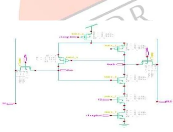
Fig 3. MTCMOS SRAM cell
Figure 4: Conventional 6T SRAM Ce ll
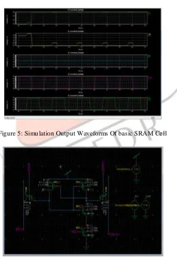
Figure 5: Simu lation Output Waveforms Of basic SRAM Ce ll
Figure 7. Simulat ion Output Waveforms of Proposed SRAM
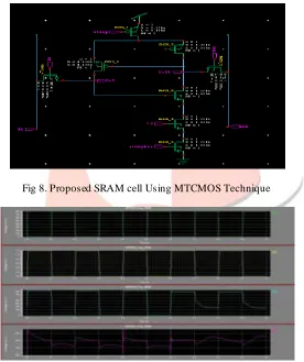
Fig 8. Proposed SRAM cell Using MTCMOS Technique
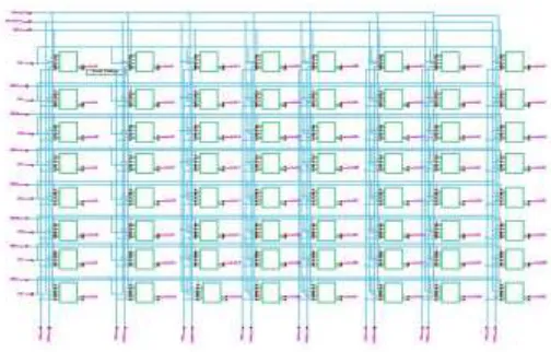
Fig 11. 8x8 SRAM Using MTCMOS SRAM cell V. RESULTS
The project concentrates on minimizing the power consumption and the complications which arise while designing memories in nm domain. The difficu lty arises due to the scaling of devices which elevates leakage current and hence the power dissipation. D ue to scaling, process variations have also come up as one of the major challenges.
In the presence of process voltage variations and temperature, this work aims at minimizing the power consumption.
Circuit TEMPERATURE(deg Centigrade‘s)
0 10 25 40 55 70
Conventio nal 6T SRAM Cell Power consumption 1.674253e -006 watts 1.863914e -006 watts 1.131169e -006 watts 1.37128e-006 watts 2.582795e -006 watts 2.582795e -006 watts Delay 9.98e-008 1.0024e
-007
1.002e-007 9.9666e -008
1.002e-007 9.9966e -007 Proposed 6T SRAM Cell Power consumption 4.521297e -007 4.902393e -007 5.439057e -007 5.952229 e-007 6.515881e -007 7.070792e -007 delay 1.0001e
-007
1.0002e -007
1.000e-007 1.0001e -007 1.0001e -007 1.0001e -007 MTCMOS based SRAM cell Power consumption 3.050317e -007 3.474972e -007 4.033006e -007 4.638165 e-007 5.103860e -007 5.547806e -007 delay
-5.0177e-010 -5.1708e-010 -5.1256e-010 -5.125e-010 -5.1954e-010 -5.2240e-010 8*8 SRAM Memory Power consumption 7.96537e-004 7.824819e -004 7.959768e -004 8.141263 e-004 8.330799e -004 8.433718e -004 Delay
-1.5552e-009 -1.6570e-010 -1.5069e-010 -1.439e-010 -1.4390e-010 -1.3804e-010 8*8 MTCMOS SRAM Memory Power consumption 5.362387e -005 5.921087e -005 5.921087e -005 6.216407 e-005 6.517123e -005 6.794650e -007 delay 2.9851e
-010 2.8927e -010 2.6814e -010 2.5286e -010 2.4600e -010 1.9749e -010 VI. CO NCLUSIONS
This project presents an SRAM cell with very low power consumption and reduces the leakage current. The effect of PVT variations on the performance metrics of the proposed cell is studied. Keeping all constraints in mind, it can be concluded t hat the proposed SRAM cell is a good contender for low powe r applications in nanometer regime.
REFER ENC ES
[1
] A. Islam and M. Hasan, ―Leakage Characterization of 10T SRAM Cell‖, IEEE Transaction s on Electron Dev ices, Vol. 59 No3, March2012.[2] Y. Y. Wang, Z.O. Wang, L.J. Zhang, ―A New 6-Transistor SRAM Cell for Low Power Cache Design‖, IEEE Conf. on So lid State and Integrated Circuit Technology, Oct., 2012, pp. 1 -3.
[4] Z. Liu and V. Kursun, ―Characterisation of a novel nine transistor SRAM cell,‖ IEEE Trans. VLSI Syst., Vol. 16, no. 4, pp . 488-492, April 2008.
[5] J. M. Rabaey, A. Chandrakasan, and B. Nikolic, in Dig ital Integratí Circuits: A Des ign Perspective, 2nd ed. New De lhi, India:Prentice- Ha ll, 2005.
[6] R. Vaddi, S. Dasgupta, and R. P. Agarwal, ―Dev ice and circu it codesign robustness studies in the subthreshold logic for ultralow-power applica - tions for 32 n m CMOS,‖ IEEE Trans. Electron Devices, vol. 57, no. 3, pp. 654–664, Ma r. 2010. [7] J. P. Ku lkarni, K. Kim, and K. Roy, ―A 160 mV robust Schmitt trigger based subthreshold SRAM,‖ IEEE J. Solid -State Circuits, vol. 42, no. 10, pp. 2303– 2313, Oct. 2007.
[8] M. Mamid ipaka et.al ―Leakage Power Estimation in SRAMs,‖ Motorola Co., USA, Sept. 2003.