Development of Application Dependent Adder
Nidhi J. Chandak Prof. G. A. Morankar
RCOEM, Nagpur RCOEM, Nagpur
Abstract
In high speed VLSI applications adders play important role. According to conventional studies much research is done on various parameters like speed, area, and power. Considering recent scenario optimization of all parameters is needed, this gives rise to idea of hybrid systems. Thus in this work two new hybrid carry select adders are used involving the carry select and section carry based carry look ahead sub adders. Performance of proposed designs is studied under Verilog HDL. As there is tradeoff between the performance parameters of adder such as area, power and delay. To overcome this problem the concept of reconfigurable hybrid system is put forward. In this paper reconfigurable hybrid system is proposed involving three different adders delivering optimized area, power and delay individually according to user’s application.
Keywords: Carry select adder, Reconfigurable, Verilog
________________________________________________________________________________________________________
I. INTRODUCTION
Adder is the basic building block of every arithmetic and logical operations. There are various types of adder already exist i.e. Ripple carry adder (RCA), Carry look ahead adder (CLA), Carry select adder (CSLA), Carry save adder (CSA) and so on. So there is need to concentrate on the various performance parameter of adder such as speed, area, power and delay. Among all these adders CSLA provides the good compromise between low area occupancy of RCA and High speed performance of CLA. This is the only reason that we are focusing on CSLA. Also Carry select adder (CSLA) belongs to the family of high speed square-root time adders. Carry select adders are realized using the following:
1) Full adders and 2 : 1 multiplexers.
2) Full adders, binary to excess 1 code converters, and 2 : 1 multiplexers 3) Sharing of common Boolean logic.
4) Carry select adder is classified as Homogeneous and Heterogeneous CSLA. It has been widely implemented using the following topologies and computational elements:
1) Conventional CSLA
2) CSLA with Binary to excess converter. (BEC) 3) CSLA based on common Boolean logic (CBL) sharing 4) Hybrid CSLA and CLA structures
5) Hybrid CSLA and CLA including BECs
Ripple Carry Adder (RCA)
Fig. 1: 8- bit RCA [1]
Carry Look Ahead Adder (CLA)
Fig. 2: 4-Bit Conventional & Section Carry Based Carry Look ahead Adder[1]
Carry look ahead adder solves the carry delay problem by calculating the carry signals in advance based on input signal. Therefore CLA is faster than RCA. Carry look ahead adder reduces the carry delay by reducing the number of gates through which a carry signal must propagate in the generation and propagation stage. Carry logic block gets very complicated for more than 4-bits.Section-carry based CLAs (SCBCLAs) were proposed as an alternative to conventional CLAs for a 32-bit addition operation, the SCBCLA was found to exhibit reduced propagation delay than the conventional CLA by 15.2%.In conventional CLA all the four carries generated by carry logic block are used but in Section-carry based CLAs (SCBCLAs) only the last carry i.e. C4 generated by CLB is used for sum generation. As in SCBCLA the concentration is only on last carry generated so propogation delay of SCBCLA gets reduced than conventional CLA.
The carry select adder generally consist of two RCA and multiplexer. Here the input partitioning is used i.e. the least significant 4- bits were generated using RCA method and MSB 4- bits using CSLA. The carry generated by 4-bits RCA is served as select input for mux. As two RCA were used for MSB 4-bits the sum will be generated on basis of carry input selected. Carry Select Adder (CSLA) architecture consists of independent generation of sum and carry i.e., Cin=1 and Cin=0 are executed parallely. Depending upon Cin, the external multiplexers select the carry to be propagated to next stage. Further, based on the carry input, the sum will be selected. Hence, the delay is reduced.
In the rest of this paper, section 2 discusses the basic architectures of three different adders namely hybrid CSLA, CSA-BEC and CSA-CBL for minimum delay, area and power respectively. Section 3 deals with concept of reconfigurable system. The comparison and simulation results put forward in section 4 and section 5 consist of conclusion.
II. PROPOSED WORK
Hybrid Carry Select Adder
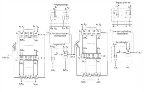
The proposed work consists of implementation of 32 bit Hybrid CSLA with input bit partitioning technique. CSLAs can be implemented on the basis of uniform or non-uniform primary input partitions accordingly they are labelled as “uniform” or “non-uniform”. “Input partitioning” basically means splitting up of the primary inputs into groups of inputs so as to pave the way for addition to be done in parallel within the partitions; Referring to Figure 1, it can be seen that 32 bit inputs have been split into four uniform groups of 8-input pairs; thus it can be said that the 32-bit CSLA is realized according to a 8-8-8-8 input partition.32-bit hybrid CSLAs incorporating a SCBCLA in the first 8- least significant stage with inputs (a0b0 – a7b7) producing the requisite sum as (sum0 –sum7) followed by Carry select Adder block with next stage of least significant bits(a8b8-a15b15). SCBCLA blocks constitute three functional blocks: propagate generate logic, look ahead carry generator, and the sum producing logic. The SCBCLA, the sum producing logic consists of full adders and an XOR gate, with the XOR gate providing the sum of the primary inputs a7,b7 and c7. While rippling of carries occurs internally within the carry-propagate adder constituting the SCBCLA and producing the requisite sums, the look ahead carry signal corresponding to an adder section is generated independently (in parallel) and serves as the look ahead carry input for the successive CSLA stage. Similarly, above processes is repeated for the remaining 16 input bits.
Conventional Carry Select Adder
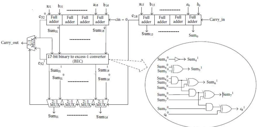
Fig. 2: 32 bit conventional CSLA using BEC logic (CSLA_BEC type)
Conventional CSLA architecture involving CSLA and BEC was implemented with the intention of minimizing the maximum area.3 uniform input partitions (4-4-4-4-4-4- 4-4, 8-8-8-8, and 16-16) were considered for realizing the 32-bit CSLAs. Above table shows the variations in area corresponding to different primary input partitions for the six CSLA types. Figure portrays the 32-bit CSLA containing full adders, 2: 1 MUXes, and BEC logic, henceforth identified as “CSLA BEC”. It also shows the internals of the 5-bit BEC, which is depicted by the circuit shown within the oval. The CSLA BEC is rather different from the CSLA in that instead of having an RCA with a presumed carry input of 1 in the more significant nibble position, the BEC circuit is introduced. The BEC logic adds binary 1 to the least significant bit of its binary inputs and produces the resultant sum and carry as output. As seen in Figure the BEC accepts as inputs the sum and carry outputs of the RCA having a presumed carry input of 0, adds binary 1 to this input, and produces the resulting sum and carry overflow as output. Now the correct result exists between choosing the output of the RCA with a presumed carry input of 0 and the output of the BEC logic. The carry output 𝑐16 of the least significant RCA is used to determine the correct set of the most significant nibble position sum and carry outputs.
Carry select adder using common Boolean logic
In proposed work, an area-efficient carry select adder by sharing the common Boolean logic term to remove the duplicated adder cells in the conventional carry select adder. In this way, it save many transistor counts and achieve a low Power. Through analyzing the truth table of a single-bit full adder, To find out that the output of summation signal as carry-in signal is logic "0" is the inverse signal of itself as carry-in signal is logic "I ".
To share the common Boolean logic term, it only needs to implement one OR gate with one INV gate to generate the Carry signal and summation signal pair. Once the carry-in signal is ready, then select the correct carry-out output according to the logic state of carry-in signal.
As compared with the regular Carry Select adder, the proposed CSLA is little bit faster, but the speed is nearly equal. The delay time in our proposed adder design is also proportional to the bit number N however, the delay time of multiplexer is shorter than that of full adder. The Proposed CSLA is Area efficient & low power, but the speed equal to the Regular CSLA.
III. RECONFIGURATION SYSTEM
As per the title, application dependent system is developed consisting of three different adders for minimum delay, area and power. Proposed system is application dependent with which allows user to select any one adder amongst described in previous section. Addition of two 32 bit numbers is performed by any one adder selected by select inputs. User can select any adder type as per application purpose.
IV. RESULTS
Comparative analysis of different adder configuration performed using Verilog HDL language. Synthesis tool used Xilinx ISE and Spartan3 Family.
Table – 1
Comparison of Adders for Area, Delay and Power. Adders Area (BELs) Delay (ns) Power (w)
Hybrid CSLA 98 10.231 0.00547
CSLA-BEC 64 23.404 0.00514
CSLA-CBL 106 11.915 0.00481
Thus considering comparison table numerous combinations are possible. Synthesis report provides value for area, delay and power for different configurations.
V. CONCLUSION
Application dependent adder system comprising of carry select technique which belongs to family of high speed square root time adders is designed using verilog module. Proposed system performs addition of two 32 bit values considering any one CSLA based adder configuration like HYBRID CSLA, CSLA_BEC, and CSLA_BEL. Adder configurations were selected considering min delay, area and power. Designed verilog module is synthesis using Xilinx ISE tool and reports for delay is summarized for all configuration thus user can select any combination according to application amongst numerous combination possible.
REFERENCES
[1] V. Kokilavani,1 K. Preethi,1 and P. Balasubramanian “FPGA-Based Synthesis of High-Speed Hybrid Carry Select Adders” Hindawi Publishing
Corporation Advances in Electronic Volume 2015, Article ID 713843.
[2] Ms. S.Manjui, Mr. V. Sornagopae” An Efficient SQRT Architecture of Carry Select Adder Design by Common Boolean Logic.” 2013 IEEE
[3] V. Kokilavani, P. Balasubramanian, and H. R. Arabnia, “FPGA realization of hybrid carry select-cum-section-carry based carry lookahead adders,” in Proceedings of the 12th International Conference on Embedded Systems and Applications, pp. 81–85,2014.
[4] B. Ramkumar and H. M. Kittur, “Low-power and area-efficient carry select adder,” IEEE Transactions on VLSI Systems, vol. 20, no. 2, pp. 371–375, 2012.
[5] I.-C.Wey, C.-C.Ho, Y.-S. Lin, and C.-C. Peng, “An area-efficient carry select adder design by sharing the common boolean logic term,” in Proceedings of
the International MultiConference of Engineers and Computer Scientists (IMECS '12), vol. 2, pp. 1091– 1094, March 2012.
[6] Y. Wang, C. Pai, and X. Song, “The design of hybrid carrylookahead/ carry-select adders,” IEEE Transactions on Circuits and Systems II: Analog and
Digital Signal Processing, vol. 49, no. 1, pp. 16–24, 2002.
[7] G.A. Ruiz, “New static multi-output carry lookahead CMOS adders,”IEE Proc. Circuits, Devices and Systems, vol. 144, no. 6, pp. 350-354,1997.
[8] J.B. Kuo, H.J. Liao, H.P. Chen, “A BiCMOS dynamic carry lookaheadadder circuit for VLSI implementation of high-speed arithmetic unit,”IEEE J. of
Solid-State Circuits, vol. 28, no. 3, pp. 375-378, 1993.
[9] C.-C. Wang et al., “A low power high-speed 8-bit pipelining CLA design using dual-threshold voltage domino logic,” IEEE Trans. OnVLSI Systems, vol.
16, no. 5, pp. 594-598, 2008.
[10] G. Yang et al., “A 32-bit carry lookahead adder using dual-path all-N logic,” IEEE Trans. on VLSI Systems, vol. 13, no. 8, pp. 992-996, 2005.
[11] R. Zlatanovici, S. Kao, B. Nikolic, “Energy-delay optimization of 64- bit carry-lookahead adders with a 240ps 90nm CMOS design example,” IEEE J. of
Solid-State Circuits, vol. 44, no. 2, pp. 569-583, 2009.
![Fig. 1: 8- bit RCA [1]](https://thumb-us.123doks.com/thumbv2/123dok_us/7817174.1664150/1.612.106.504.495.642/fig-bit-rca.webp)
![Fig. 2: 4-Bit Conventional & Section Carry Based Carry Look ahead Adder[1]](https://thumb-us.123doks.com/thumbv2/123dok_us/7817174.1664150/2.612.100.514.517.719/conventional-section-carry-based-carry-look-ahead-adder.webp)