Abstract—Smart antennas have been studied extensively this decade because of its low profile structure and formidable rate, thereby creating new and improved services at lower costs. They are extremely compatible for embedded antennas in handheld wireless devices such as cellular phones, pagers etc. Because of its versatility, Smart antenna which is designed by planer array can be used to synthesize a required pattern that cannot be achieved with a single patch element.
Index Terms—Radiation patterns, Mobile communication, planar array, PCCAD 5.0 software etc.
I. INTRODUCTION
In high-performance aircraft, spacecraft, satellite and missile application, where size, weight, cost, performance, ease of installation, and aerodynamic profile are constraints, so low profile antennas may be required. Presently there are many other government and commercial applications, such as mobile, radio and wireless communications that have similar specifications .To meet these requirements “smart antennas” have been researched extensively. This has resulted in an increase in airtime usage and in the number of subscribers. Spatial processing is the central idea of smart-antenna systems. Although it might seem that smart antennas have been recently discovered, they date back to World War II with the conventional Bartlett beamformer [1]. It is only of today’s advancement in powerful low-cost digital signal processors, general purpose processors (and ASICs—Application-Specific Integrated Circuits), as well as innovative software-based signal-processing techniques (algorithms), that smart antenna systems have received enormous interest worldwide. To approach the feature, design smart antenna by microstrip patch antenna array [2]. Quality factor (Q) of microstrip antennas is a very high. Quality factor can be reduced by increasing the dielectric substrate. But due to increasing thickness, unwanted power loss occurs by the surface wave. However, this surface waves can be minimized by the use of photonic bandgap structures [3].
Recent studies on microstrip antennas have primarily concentrated on the improvement of bandwidth and on the design of multifunction operations [4]–[7]. As a result, almost 100% bandwidth in terms of VSWR and dual-band
Manuscript received May 8, 2011; revised December 1, 2011.
Japatosh Mondal is with the Department of Electrical and Electronic Engineering, Prime University, Dhaka (e-mail: jopobabu_eee05@ yahoo.com).
Sobuj Kumar Rayis with the Department of Electrical and Electronic
Engineering, International University of Business Agriculture and Technology (IUBAT), Uttara, Dhaka, Bangladesh (e-mail: sobuj_kumar_ray@ yahoo.com).
Md.Shah Alam is with EEE of RUET. (e-mail: sumon01146@yahoo. com)
Md. Mezanur Rahman (e-mail:[email protected]).
operations for GSM900 and GSM1800 WLAN services have been success-fully accomplished and demonstrated.
II. MICROSTRIP ANTENNA AND FEEDING METHOD
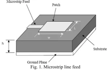
A microstrip antenna is a metallic patch on top of a layer of dielectric substrate with a backing ground plane. It consists of four parts like a very thin flat metallic region often called patch, a dielectric substrate, a ground plane and a feed which supplies the element RF power.
Patch is a very thin flat metallic region .The longest dimension of the patch is typically about a third to a half of a free-space wavelength. So the patch starts to radiate. A commonly used dielectric substrate for microstrip antenna is polytetrafluorel (PTFE). A relative dielectric constant around 2.5 is typical. The ground plane is a printed circuit board. Monolithic Microwave Integrated Circuits (MMICs) combine microstrip antennas and associated circuitry in very compact form with applications at frequencies from 50 MHz to l00GHz.
There are four feeding mechanisms.
A. Microstrip-Line Feed
The microstrip line feed is easy to fabricate, simple to match by controlling the inset position and rather simple to model. However as the substrate thickness increases surface waves and spurious feed radiation increase, which for practical designs limit the bandwidth (typically 2-5%) [2].
Fig. 1. Microstrip line feed
B. Coaxial Probe Feed
Coaxial probe feeds (Fig. 2), where the inner conductor of the coax is attached to the radiation patch while the outer conductor is connected to the ground plane, are also used. The coaxial probe feed is also easy to fabricate and match and it has low spurious radiation. However, it also has narrow bandwidth and it is more difficult to model, especially for thick substrate [2].
C. Aperture -Coupled Feed
Both the microstrip feed line and the probe possesses inherent asymmetries which generate higher order modes which produce cross-polarized radiation. To overcome some of these problems, non contacting aperture coupling feeds,
Design Smart Antenna by Microstrip Patch Antenna Array
as shown in Fig. 3, have been introduced. The aperture coupling is the most difficult of all four coupling methods to fabricate and it has narrow bandwidth. This coupling consists of two substrates separated by a ground plane. The aperture coupling consists of two substrates separated by a ground plane. On the bottom side of the lower substrate there is a microstrip feed line whose energy is coupled to the patch through a slot on the ground plane separating the two substrates. This arrangement allows independent optimization of the feed mechanism and the radiating element [2].
D. Proximity-Coupled Feed
In proximity-coupled feed method, two dielectric substrates are placed in such way that the feed line is between the two substrates and the radiating patch is on top of the upper substrate. The proximity-coupled method has the largest bandwidth (as high as 13%), is somewhat easy to model and has low spurious radiation. However its fabrication is somewhat more difficult [2].
E. Linearly Polarized Microstrip Antennas
Fig. 1 shows a patch antenna, in which the patch is rectangular and it is thus called rectangular patch antenna. When feed, a standing wave will occur as shown in Fig. 5, but some of the field will “leak out” around the edges of the patch. This is the so called fringing field. In the figure, we can see that the electric field on the left side outside the patch is going into the patch and on the other side leaving the patch. [8]
Fig. 2. Coaxial probe feed
Fig. 3. Aperture –Coupled
Fig. 4. Proximity-Coupled feed
Fig. 5. Two radiating slots used to model a microstrip patch antenna. [9]
III. DESIGN PROCESS
The first step of this process is to design an antenna suitable for the network/communication requirements such as the required beamwidth to maintain a tolerable bit error rate (BER) or throughput. It includes single element design (e.g., dimensions, material, and geometry), and array design (e.g., configuration, inter-element spacing, and number of elements). After the antenna design step is complete, the second step is to select an adaptive algorithm.
Two aperture types antenna Single Element Rectangular Patch and Square Patch of dimensions w along X and L along Y and located in the Z=0 plane it’s shown in the Fig. 8.
Fig. 6(a). Rectangular aperture
Fig. 6(b). Square aperture
(a) (b)
Fig. 7. Comparison of radiation pattern of (a) Rectangular aperture type and (b) Square aperture type
that case, interference problem in many users can be limited in rectangular aperture type antenna. So they can direct the main beam toward the pilot signal or SOI while suppressing the antenna pattern in the direction of the interferers or SNOIs. Consequently, for smart antennas, we use rectangular patch antenna array.
Microstrip line is that which provides one free and accessible surface on which solid state devices can be placed. All electrical and electronic devices with high power output commonly use conventional lines, such as coaxial lines or waveguides, for power transmission. However the microwave solid-state device is usually fabricated as a semiconductor chip with a volume on the order of 0.008 to 0.08mm quake. The method of applying signals to the chips and extracting output power from them is entirely different from that used for vacuum tube devices. Microwaves integrated circuits with microstrip lines are commonly used with the chips. [10]
Fig. 8. A microstrip transmission line
Practical microstrip lines (shown in figure) have width to height ratio w/h that are not necessarily much greater unity and can vary over the interval 0.1< w/h <10. Typical heights h are of the order of millimeter. Modes on microstrip lines are only quasi-transverse electric and magnetic (TEM). Radiation loss in microstrip lines is a problem. However the use of thin, high-dielectric materials considerably reduces the radiation loss of the microstrip. The characteristic impedance of a microstrip line is a function of the strip-line width, the strip-line thickness, the distance between the line and the ground plane and the homogeneous dielectric constant of the board material. Here
ε
r = dielectric constanth= height from the center of the wire to the ground plane. The equation of the characteristic impedance by comparative or an indirect method is,
) 4 ln(
60
0 h
t
Z =
(1)
IV. METHODS OF MODELING
Three methods of analysis are commonly used to evaluate microstrip antenna (MSA) parameters [11], [12]. These are: Transmission line model, cavity model, and full wave analysis.
A. Transmission Line Model of Microstrip Patch
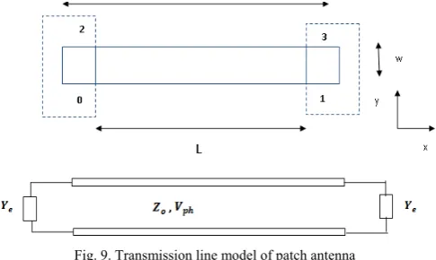
The transmission-line model is the easiest of all, it gives good physical insight. Basically the transmission line model
represents the microstrip patch antenna by two slots, separated by a low impedance (Z0) transmission line of length L [9], [11].
Fig. 9. Transmission line model of patch antenna
The voltage distributions at the edges of the microstrip patch antenna operation in the TM10 dominant mode (or
TMM0) can be obtained by using a transmission line model. For TM10 (or TMM0) mode of the microstrip patch, there is no variation of fields in the y direction. The field distribution is identical to that of a uniform transmission line of characteristic impedance Zo and Vph. The fringing fields
associated with edges 01 and 23 of the patch are taken into account by Zo and Vph. The fringing fields associated with
edges 02 and 13 are represented by lumped admittances Ye
(edge conductance) connected at the two ends [9].
B. Transmission Line Model of Microstrip Patch for Edge Admittance
Edge admittance is given by,
Ye=Ge+jBe (2)
where Be =ωCe, Ge,Be, Ce are the edge conductance, edge
susceptance and edge capacitance respectively. The edge conductance accounts for the power radiated at the radiating edges (or open ends).The edge susceptance accounts for the fringing electric field (and hence the fringing capacitance at the open end) [2].
C. Transmission Line Model of Microstrip Patch for Edge Capacitance
The edge capacitance, Ce is represented in terms of an
equivalent line length extension as shown in the following figure:
Fig. 10. Transmission line model for microstrip Patch: Edge capacitance
From the theory of open ended transmission line, the edge susceptance of microstrip patch can be expressed as [9], [11].
( )
lY C
B0 =
ω
0 = 0tanβ
Δ (3)If βΔl<<1 or Δl<<
λ
Then the edge capacitance can be approximated as
0
z v
l C
P
B = Δ (4)
where vP =ωβ , VP is the phase velocity and Z0 is the characteristic impedance.
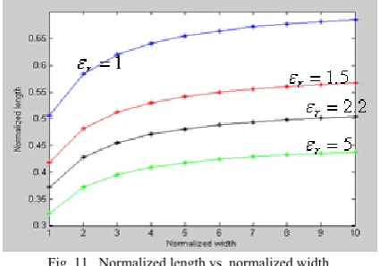
A. Normalized Length vs. Normalized Width Curve
Because of the fringing effect, electrically the patch of the microstrip antenna looks greater than its physical dimension as shown in Fig. 10. The dimension of the patch along its length have been extended on each end side by a distance
l
Δ , which is a function of dielectric constant, εr and width
to height ration (w/h) and can be expressed as [2].
Normalized length,
(
)
(
)
⎟⎠ ⎞ ⎜ ⎝ ⎛ + −
∈
⎟ ⎠ ⎞ ⎜
⎝ ⎛ + + ∈ =
Δ
8 . 0 258 . 0
264 . 0 3 . 0 412 . 0
h w h w
h l
reff
reff (5)
The Normalized Length vs. Normalized Width Curve is drawn in Fig. 11. For various values of dielectric constant, εr.
Fig. 11. Normalized length vs. normalized width.
From Fig. 11,it is seen that for a fixed normalized width, the normalized length increases with the decrease in dielectric constant and for a fixed dielectric constant the normalized length increases with the increase in normalized width.
B. Calculation of Edge Conductance
The edge conductance accounts for the power radiated at the radiating edges and can be evaluated using the equivalent magnetic current model for fringing field edges. In order to calculate the edge conductance the expressions of electric field and magnetic field are required.
In order to determine the edge or radiation conductance approximation, three ranges are taken into account which is given below [13].
Range 1: wλ0 <<1, the edge conductance becomes 2
0
90 1
⎟⎟ ⎠ ⎞ ⎜⎜ ⎝ ⎛ =
λ
w Gr
(6) Range 2: 35λ0≤w≤2λ0, the edge conductance becomes
2
0 60
1 120
1
π λ − ×
= w
Gr (7)
Range 3: 1
0 >>
λ
w w→α
The edge conductance becomes 0
120 1
λ w
Gr = (8)
Using the above three ranges the edge conductance, Gr is
plotted as a function of width to free space wavelength ration, as given below:
Fig. 12. Gr vs. for << 1
Fig. 13. Gr vs. for >> 1
C. Expressions of E-Field and H-Field Of N-Elements Linear Array
Antenna array is used to improve performances such as gain, directivity etc. In the case of patch antenna array, it can be used to scan the beam of an antenna system and perform various other functions which would be difficult with any one single element. Fig. 15 shows a rectangular patch antenna array of n-elements separated from each other by a distance d.
Fig. 14. Linear array with elements along the y-axis
D. Drawback of Linear Array
planner arrays are more attractive for these mobile devices, so we can design M×N identical elements in the xy-plane as shown in Fig. 16.
E. M×NPlanar Array
Fig. 15. Design of a M×N planar array with rectangular patches. (SOURCE: [15] )
D. DESIGN AND PARAMETER CALCULATION
The design procedure of patch antenna assumes that the specified information includes the dielectric constant of the substrate (εr=2.2), the resonant frequency (fr=10GHz) and
the height of the substrate (h=2.93mm). The necessary equations to design patch antenna [14]
The width of the patch for effective radiation can be expressed as mm f v f W r r r r 9 . 11 8585 . 11 1 2 . 2 2 10 10 2 10 3 1 2 2 1 2 2 1 9 8 0 0 0 ≅ = + × × × = + ∈ = + ∈ ∈ =
μ (9)
The effective refractive index can be expressed as
9013 . 1 9 . 11 93 . 2 12 1 2 1 2 . 2 2 1 2 . 2 12 1 2 1 2 1 5 . 0 2 / 1 = ⎥⎦ ⎤ ⎢⎣ ⎡ + − + + = ⎥⎦ ⎤ ⎢⎣ ⎡ + − ∈ + + ∈ = ∈ − − mm mm w h r r eff (10)
The extension of length of each side can be expressed as
(
)
(
)
(
)
(
)
mmmm mm mmmm mm h h w h w l reff reff 4 . 1 93 . 2 8 . 0 93 . 2 9 . 11 258 . 0 2 . 2 264 . 0 93 . 2 9 . 11 3 . 0 2 . 2 412 . 0 8 . 0 258 . 0 264 . 0 3 . 0 412 . 0 = × ⎟ ⎠ ⎞ ⎜ ⎝ ⎛ + − ⎟ ⎠ ⎞ ⎜ ⎝ ⎛ + + = × ⎟ ⎠ ⎞ ⎜ ⎝ ⎛ + − ∈ ⎟ ⎠ ⎞ ⎜ ⎝ ⎛ + + ∈ × = Δ (11)
The actual length of the patch can be expressed as
mm mm l f L ff r 8 4 . 1 2 9013 . 1 10 10 2 10 3 2 2 1 9 8 0 0 = × − × × × = Δ − ∈ ∈ = θ μ (12) Effective length of the patch can be expressed as
mm f v f L ff r ff r eff 9 . 10 9013 . 1 10 10 2 10 3 2 2 1 9 8 0 0 0 ≅ × × × = ∈ = ∈ ∈ = θ θ μ (13) θ θ θ θ π d w k
I 2 3
0
0
1 cos ] sin
cos 2 sin [ ⎟ ⎠ ⎞ ⎜ ⎝ ⎛ =
∫
(14)(
7 12)
0.59
0 = 2π ×10×10 × 4π ×10− ×8.854 ×10−
k (15)
2 1 1 120
π I
G = w>>λ (16)
θ θ θ θ θ π d L k J w k G 3 0 0 2 0 0
12 cos ( sin )sin
) cos 2 sin(
∫
⎥ ⎥ ⎥ ⎥ ⎦ ⎤ ⎢ ⎢ ⎢ ⎢ ⎣ ⎡= (17)
Because of the odd field distribution between the radiating slots for the dominant TM010 mode.
By numerically calculation, the input impedance of the patch can be expressed as
Ω =
+
= 231.3490
) ( 2 1 12 1
1 G G
Z (18)
Length of the impedance inverter
4d λ = mm r 06 . 5 4 0 = ∈
= λ (19)
Width of the impedance inverter,
mm z z h w r l 2 . 2 2 0 = ⎟ ⎟ ⎠ ⎞ ⎜ ⎜ ⎝ ⎛ − ∈ =
The characteristic impedance,
Ω =
× =
= Z1Z2 231.3490 50 107.5521
Zl (20)
where, Z2is the probe impedance =50Ω.
Fig. 16. Microstrip patch antenna
E. RADIATION PATTERNS OF E-FIELD AND H-FIELD A. Variation of Radiation Pattern Due To Change of Relative Dielectric Constant
Fig. 18 shows the effect of the dielectric constant of the substrate of the rectangular microstrip antenna on its radiation pattern. Fig.18. (a) shows the radiation pattern with the parameter h = 2.93 mm, fr =10GHz&εr =2.2. Fig. 18 (b) shows the radiation pattern with the parameter h = 2.93 mm, fr=10GHz & εr =5.
B. Variation of Radiation Pattern Due To Change of Height (H)
Fig. 19 shows the effect of the height of the rectangular microstrip antenna on its radiation pattern. Fig. 19 (a) shows the radiation attern with the parameter h=2.93mm,
GHz
fr =10 &εr =2.2 . Fig. 19(b) shows the radiation pattern with the parameter h =5 mm, fr=10GHz, εr =2.2.
C. Radiation Pattern of Single Patch Antenna
Radiation pattern of E-field and H-field for distance r=80cm are shown in Fig. 20(a) and for r=115cm are shown in Fig. 20(b).
0.2 0.4 0.6 0.8 1 30 210 60 240 90 270 120 300 150 330 180 0 E-plane 0.2 0.4 0.6 0.8 1 30 210 60 240 90 270 120 300 150 330 180 0 H-plane Fig. 18(a) 0.2 0.4 0.6 0.8 1 30 210 60 240 90 270 120 300 150 330 180 0 E-plane 0.2 0.4 0.6 0.8 1 30 210 60 240 90 270 120 300 150 330 180 0 H-plane Fig. 18(b) 0.2 0.4 0.6 0.8 1 30 210 60 240 90 270 120 300 150 330 180 0 E-plane 0.2 0.4 0.6 0.8 1 30 210 60 240 90 270 120 300 150 330 180 0 H-plane Fig. 19(a) 0.2 0.4 0.6 0.8 1 30 210 60 240 90 270 120 300 150 330 180 0 E-plane 0.2 0.4 0.6 0.8 1 30 210 60 240 90 270 120 300 150 330 180 0 H-plane Fig. 19(b)
D. Radiation Pattern Of Two Element Linear Patch Antenna
Radiation pattern of E-field and H-field for distance r=80cm are shown in Fig. 21. (a) and for r=115cm are shown in Fig. 21. (b)
From above figures we can observe that, for single patch antenna, radiation pattern spread with increases distance. But for two element linear array radiation pattern is sharp than single patch antenna and hence that radiation pattern not spread with increases distance.
E. Radiation Pattern of 2×2 Planer Array Antenna
[12]
0.01 0.02 0.03 0.04
30
210 60
240 90
270
120
300
150
330
180 0 E-plane
0.005 0.01 0.015
30
210
60
240 90
270 120
300 150
330
180 0
H-plane
Fig. 22
From Fig. 21 and Fig. 22 we can observe that, for 2×2 planer array antenna’s main lobes are sharper than linear array antenna. Moreover, radiation pattern is not dependent on distance for a certain limit. So, planner array is more suitable for smart antenna.
F. Radiation Patterns Obtained Using Pccad 5.0 Software
PCCAD 5.0 is useful software for obtaining both polar and 3-D radiation pattern. Moreover various parameters such as bandwidth, efficiency, directivity, 3-dB beam width can be calculated. The radiation pattern of E-field and H-field for single patch element using PCCAD 5.0 software is shown in Fig. 23.
Fig. 23. Radiation pattern of E-field and H-field
The following parameters are obtained using PCCAD 5.0 software:
TABLE I: PARAMETERS USING PCCAD5.0SOFTWARE
Bandwidth 9% Efficiency 99% Directivity 6.7
Beamwidth 76.6 degree for H-plane
Fig. 24. 3-D radiation pattern
The 3-D radiation pattern of a single patch element using PCCAD 5.0 software is shown in Fig. 24.
The radiation pattern of E-field for two element patch array using PCCAD 5.0 software is shown in Fig. 25.
Fig. 25. Radiation pattern of E-field
TABLE II: PARAMETERS USING PCCAD5.0SOFTWARE
Directivity 8.2
3-dB Beamwidth 73.9 degree for E-plane
The 3-D radiation pattern of two elements patch array using PCCAD 5.0 software is shown in Fig. 26.
Fig. 26. 3-D radiation pattern
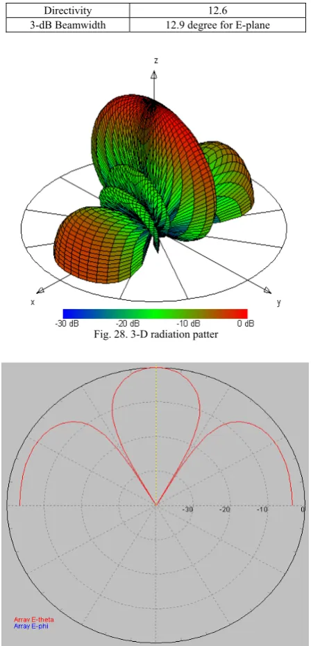
The radiation pattern of E-field for four element linear array using PCCAD 5.0 software is shown in Fig. 27.
The 3-D radiation pattern of four element linear array using PCCAD 5.0 software is shown in Fig. 28.
The radiation pattern of E-field for 2×2 planer array[12]
using PCCAD 5.0 software is shown in Fig. 29.
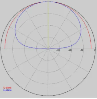
Fig. 27. Radiation pattern of E-field
TABLEIII:PARAMETERS USING PCCAD5.0SOFTWARE
Directivity 12.6
3-dB Beamwidth 12.9 degree for E-plane
Fig. 28. 3-D radiation patter
Fig. 29. Radiation pattern of E-field
TABLEIV:PARAMETERS USING PCCAD5.0SOFTWARE
Directivity 12.7 3-dB Beamwidth 28.1 degree for E-plane
Fig. 30. 3-D radiation pattern
F. CONCLUSION
Therefore we mention that, for 2×2 planer array antenna’s main lobes are sharper than linear array antenna. Moreover, radiation pattern is not dependent on distance for a certain limit. So, planner array is more suitable for smart antenna. For highly versatile uses 4
×
4 or 8×
8planer is necessary to determine the array configuration is most attractive for a wireless device in a Mobile Ad hoc NETwork (MANET) [15]. Limitation of this system is that it tends to increase the cost and the complexity of the hardware implementation, and the other is that it increases the convergence time for the adaptive algorithms, thereby reducing valuable bandwidth.REFERENCES
[1] Krim and M. Viberg, “Two Decades of Array Signal Processing
Research: The Parametric Approach”, IEEE Signal Process. Mag., pp. 67–94, July 1996.
[2] Constantine A. Balanis. Willey and Sons, “Antenna Theory”, 2nd
edition (1997), Chap 14.pp.722-783, ISBN 978-81-265-1393-4.
[3] K. Rambabu, M. Alam, J. Bornemann and M. A. Stuchly, “Compact
Wideband Dual-Polarized Microstrip Patch Antenna”, IEEE. 2004. www.ece.uvic.ca/~jbornema/Conferences/102-04aps-kabs.pdf.
[4] N. Herscovici, “New considerations in the design of microstrip
antennas,” IEEE Trans. Antennas and Propagation, Vol. 46, pp. 807– 812, June 1998.
[5] M. Kijima, Y. Ebine, and Y. Yamada, “Development of a
dual-frequency base station antenna for cellularmobile radios,” IEICE
Trans. Commun., Vol. E82-B, pp. 636–643, Apr. 4, 1999.
[6] N. Herscovici, “A wide-band single-layer patch antenna,” IEEE Trans. Antennas Propagat., Vol. 46, pp. 471–474, Apr. 1998.
[7] J.-Y.Jia-Yi Sze and K.-L.Kin-Lu Wong, “Slotted rectangular
microstrip antenna for bandwidth enhancement,” IEEE Trans.
Antennas Propagat., Vol. 48, pp. 1149–1152, Aug. 2000.
[8] W. L. Stutzman. Johm Willy & sons, inc., “Theory and Design
Antenna”, 2nd edition (1998), Chap 5, pp.16-20.
[9] P. Bhartia, K. V. S. Rao, and R. S. Tomar, “Millimeter-Wave Microstrip and Printed Circuit Antennas”, ARtech House, Boston, MA, (1991).
[10]William F. Richards “Microstrip Antennas”, 2nd edition, University
[11]R. W. Dearnley, “A Broadband Transmission Line Model for a
Rectangular Microstrip Antenna” IEEE Trans., Antennas and
propagation, Vol. AP 37, No. 1, pp. 6 - 15, January 1989.
[12]Jani Ollikainen and Pertti Vainikainen, “Radiation and Bandwidth
Characteristics of Two Planar Multistrip Antennas for Mobile
Communication Systems”, IEEE Vehicular Technology Conference,
Ottawa, Ontario, Canada, Vol. 2, pp. 1186-1190, 1998.
[13]R. F. Harrington, “Time Harmonic Electromagnetic fields”,
McGraw-Hill Book Co.p.183, (1961).
[14] E. O. Hammerstad, “Equations for Circuit Design”, Proc. Fifth
European Microwave Conf., pp.268-272, September 1975.
[15]S. Bellofiore, J. Foutz, R. Govindarajula, I. Bahceci, C. A. Balanis, A. S. Spanias, J.M. Capone, and T. M. Duman, “Smart Antenna System Analysis, Integration and Performance for Mobile Ad-Hoc Networks
(MANETS)”, IEEE Trans. Antennas Propagat, Vol. 50, No. 5, pp.
571–581, May (2002).
Mr. Japatosh Mondal was born in Khulna,
Bangladesh. Mr. Mondal received his Bachelor degree in Electrical and Electronic Engineering from Rajshahi University of Engineering and Technology (RUET), Rajshahi, Bangladesh in April 2010. Now he is a faculty in The Department of Electrical and Electronic Engineering, Prime University, Bangladesh, (www.primeuniversity.edu. bd). The major fields of study of power system control, software based electronics circuit, fields and waves with antenna radiation and fiber optics.
Mr. Sobuj Kumar Ray was born in Bogra,
Bangladesh. Mr. Ray received his Bachelor degree in Electrical and Electronic Engineering from the Rajshahi University of Engineering and Technology (RUET), Rajshahi, Bangladesh in April 2010. Now he is a faculty in the department of Electrical and Electronic Engineering, International University of Business Agriculture and Technology (IUBAT), Uttara, Dhaka, Bangladesh (www.iubat. edu). The major fields of study of Mr. Ray comprise fields and waves with antennaradiation, power system control.
Mr. Md. Shah Alam was born in Rangpur,
Bangladesh. Mr. Alam received his Bachelor degree in Electrical and Electronic Engineering from the Rajshahi University of Engineering and Technology (RUET), Rajshahi, Bangladesh. Now he is a faculty in the department of Electrical and Electronic Engineering, RUET.
Mr. Md. Mezanur Rahman, was born in
![Fig. 5. Two radiating slots used to model a microstrip patch antenna. [9]](https://thumb-us.123doks.com/thumbv2/123dok_us/1366810.1646272/2.595.321.512.54.146/fig-radiating-slots-used-model-microstrip-patch-antenna.webp)
![Fig. 17. Microstrip patch 2×2 planer array[12]](https://thumb-us.123doks.com/thumbv2/123dok_us/1366810.1646272/5.595.51.551.56.840/fig-microstrip-patch-planer-array.webp)